Investigating the Talbot Effect in Arrays of Optical
Dipole Traps for Neutral Atom Quantum Computing
A Senior Project presented to
the Faculty of the Physics Department California Polytechnic University, San Luis Obispo
In Partial Fulfillment
of the Requirements for the Degree Bachelor of Science
By
Sergio Aguayo
Abstract
Contents
List of Figures 4
1 Introduction 5
2 Theory 6
2.1 Realization of Qubits . . . 6
2.2 Neutral Atom Traps . . . 6
2.3 Pinhole Diffraction . . . 8
2.4 Talbot Effect . . . 10
2.5 Experimental Methods . . . 11
3 Computational Methods 14 3.1 Vetting Traps . . . 14
3.2 Trap Investigation . . . 15
4 Results 17
5 Conclusion 19
6 References 20
List of Figures
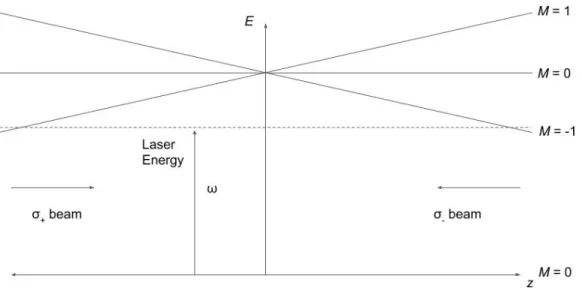
1 Talbot carpet for grating. This diagram was made using a crude model. Monochromatic light reflecting from a grating was modeled as 11 plane waves separated by 2 micrometers for each grating slit, and each slit is separated with a center to center distance of 200 micrometers. The Talbot effect can be seen at the 0.10 m mark and the 0.20 m mark. . . 11 2 1D representation of Zeeman splitting in MOT. This figure shows the gap
between two states in the energy structure of an atom. The lower state is represented by the z-axis while the higher state is represented by three lines labeled M =−1, M = 0, and M = 1. Due to the Zeeman effect, σ+
is closer to resonance with atoms on the left side of the center, while σ− is
closer to resonance with atoms on the right side of the center. This causes atoms to be driven towards the center [9]. . . 13 3 Trap vetting plots. The figures are captioned with their respective values
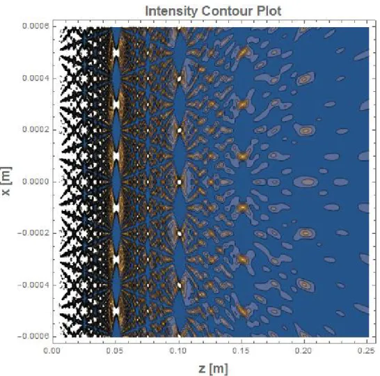
for the radius of the pinholea, the period of the arrayd, and the number of pinholes in the array n. These plots illustrate a large range in the amount of presence the Talbot effect exhibits. (a) shows a large presence of the Talbot effect, (b) shows a moderate amount of presence, (c) shows a small amount of presence, and (d) shows no presence. . . 15 4 Talbot carpet for one-dimensional pinhole array. This contour plot was
calculated with pinhole radiusa= 10 µm, pinhole periodd= 110µm, and number of pinholes n= 21. The array of pinholes, located at the origin, is located to the left of this plot. Its replicated image can be seen in the center. 16 5 Trap vetting results. Table (a) is the result for radius a = 10 µm, table
1
Introduction
Quantum computers are devices which can perform tasks unreachable for classical com-puters. The property separating quantum computers and classical computers are their units of data: qubits and bits. Bits are units with two possible values–0 or 1; on the other hand, qubits take advantage of superposition to create states characterized as linear combinations of 0 and 1. Just like with classical computers, quantum computers have logic gates that can be used to perform calculations or solve computational problems. Logic gates can involve any number of qubits, requiring that qubits be entangled and that individual qubit’s states be manipulated. This necessitates precise control of qubits, meaning that there are certain criteria that must be met by the hardware infrastructure of a quantum computer.
There are five requirements needed for implementing a quantum computer: (1) A scalable physical system with well characterized qubits; (2) the ability to initialize the state of qubits to a simple state; (3) long decoherence times that are much longer than gate operation times; (4) a universal set of quantum gates; (5) the ability to measure qubit states [1].
While there are several different ways to implement a quantum computer, the one we focus on uses neutral atoms. Neutral atoms have the advantage of being relatively stable compared to the components of other implementations. This leads to an advantage in (3)–long decoherence times–and in (1)–the ability to scale the system. Since neutral atoms are so stable, not only do we get long decoherence times, we are also able to scale a system to a large number in a small amount of space, since nearby atoms rarely interact with one another [2].
The aim of this project is to model possible traps that will fulfill the listed criteria for implementing a quantum computer. This will be accomplished using atomic dipole traps. Atomic dipole traps utilize electric dipole interaction with light [3]. These traps are created by passing a laser beam through a pinhole, which produces a diffraction pattern. The intensity gradient of these diffraction patterns interact with the induced dipole moment in a neutral atom to create a potential well. The minima of the potential well can be used as an atom trap [3].
2
Theory
2.1
Realization of Qubits
The five criteria listed in Section 1 create restrictions for what our atom traps can look like. These restrictions and our ideal trap configurations will be discussed in this section. Criterion (1) requires that our system be scalable. To do this, the trap created should have well defined locations. An example of what traps may look like are two-dimensional rectangular arrays or three-dimensional rectangular arrays.
Criteria (2), (4), and (5) require that we have the ability to initialize qubits and have the ability to measure their states. This means that it is advantageous that each atom be individually addressable. Atoms can be individually addressed using lasers. In a two-dimensional array, addressing individual atoms can be done by shining a laser on an atom perpendicular to the plane of the array. Descriptions of two-dimensional arrays can be seen in [4] and [5]. Addressing individual atoms in a three-dimensional array is more of a challenge, but it is achievable. Addressing individual atoms in a three-dimensional array has been achieved using pulsed microwaves and two laser beams [2].
With these criteria in mind, we can plan what atom traps can look like. Two-dimensional and three-Two-dimensional arrays are both viable options and have been shown to be able to meet the listed criteria.
2.2
Neutral Atom Traps
The type of neutral atom trap we are using is an optical dipole trap. As discussed in Section 1, optical dipole traps utilize the interaction between the intensity gradient of light and the induced electric dipole of a neutral atom. In this section, we will detail this interaction.
Light used in an optical dipole trap is far-detuned from the resonance frequency of a transition in the atom. This allows us to neglect forcing from radiative pressures (the pressure created by recoils due to photon absorption) [3] and to treat the light classically as a harmonic driving field with angular frequency ω. This electric field E induces an electric dipolep in the atom.
The electric field is written in complex notation: E(r, t) = Eoe−iωt. Dipole moments
are defined as p = qd, where q is the charge at either end of the dipole, and d is the displacement vector from the negative charge to the positive charge. If we take the nucleus of the atom as the center of our system andxas the position vector of the electron orbiting the nucleus, then we haved =−x, which givesp=−ex, whereeis the elementary charge. We can solve for the position vector of the electron by treating the motion of the electron as a driven and damped oscillation around the nucleus. This gives us a differential equation
me
d2x
dt2 +meΓω
dx
dt +meω
2
where me is the mass of an electron, Γω is the radiative decay rate of the energy of an
electron oscillating at an angular frequencyω in an atom, andωo is the resonance angular
frequency of the atom [6]. Solving this equation gives
x=− e
me
1 ω2
o −ω2−iωΓω
Eoe−iωt. (2)
Which gives
p= e
2
me
1 ω2
o−ω2−iωΓω
Eoe−iωtxˆ. (3)
We can simplify the expression forp by introducing variable α, defined as
α=
meωo2−ω2−iωΓω
,
e2 1
(4)
which simplifiesp to
p=αE. (5)
Now that we have established the relationship between the dipole moment and the electric field, we can move on to describing the potential energy of our trap. The potential energy of a dipole moment in an electric field is given by
Udip =−p·E. (6)
However, since our electric field and dipole oscillate so rapidly, only their time averages are relevant [6]. Also, since our atom is an induced dipole moment, we need to introduce a factor of 1/2 [6]. This gives
Udip =−
2hp·Ei. 1
(7)
Since our dipole moment and electric field are in complex notation, we need to find their real parts in order to use them in theUdip equation. The real part of the electric field is
given by
Re(E) =Eocos(ωt)ˆx, (8)
and the real part of the dipole moment is given by
Re(p) = Re(α) Re(E) + Im(α) Im(E)
=Eo(Re(α) cos (ωt)−Im(α) sin (ωt)) ˆx. (9)
Plugging Re(p) and Re(E) into equation 7, we obtain
Udip =−
1 4
e2
me
ω2
o−ω2
(ω2
o −ω2)2+ω2Γ2ω
This expression can be simplified by introducing the linewidth of the atom at resonance Γ and the saturation field Es. We start with Γω, the radiative decay rate of the energy
2 2
of an electron oscillating at an angular frequency ω defined as Γω = 6πe ω 3. For an
omec atom at resonance (ie. ω=ω ), we have Γ = e2ω2o
o 6π 3. Putting these together, we get an
omec expression for Γω in terms of Γ:
2
Γω =
ω ω2
o
Γ. (11)
Now we consider the saturation fieldEs. The expression for the saturation field is [6]
Es2 = ~Γ
2m
eωo
e2 , (12)
where~is Planck’s constant. Substituting the expressions for the saturation field and the linewidth of the atom at resonance into Udip yields
Udip =−~
Γ2ω
o
4
ω2
o −ω2
(ω2
o −ω2)
2
+ωω32
o 2 Γ2 E2 E2 s . (13)
Further simplification of this expression
can be achieved by considering two
approx-2
imations: the first is (ωo2−ω2 2) >> ωω32 Γ2, and the second is that ωo and ω are the
o
same order of magnitude. With these approximations we simplify Udip to
Udip = ~
Γ 8 Γ ∆ E2 o
E2, (14)
where ∆ is the amount of laser detuning ω−ωo.
2.3
Pinhole Diffraction
In order to properly model our trap, we need to calculate the electric field of the diffraction pattern. This is done by using Fresnel scalar diffraction theory. Our start point for our calculation is to consider the Fresnel-Kirchhoff diffraction integral. This equation gives the electric fieldE of the diffracted light at point P1 and is defined as
E(P1) =
kz1
i2π Z Z
So
Ez=0
eikρ
ρ2 dxodyo, (15)
wherek is the wavenumber of the light used,So is the surface of the pinhole, Ez=0 is the
electric field on the plane of the pinhole, and
ρ= (x1−x0)2+ (y1−y0)2+z21,
q
where the variables with subscript 0 are in the plane of the pinhole and the variables with subscript 1 are at the point of interestP1.
If we use binomial expansion on ρ it becomes
ρ=
∞
X
n=0
1/2
n
((x1−x0)2+ (y1−y0)2)n
z21n−1 . (17)
By taking approximationsz13 >> 4πλ((x1−x0)2+ (y1−y0)2 2) and ρ2 ≈z12 we can reduce
kρinto
kρ= 2π
λ z1+ 1 2
(x1−x0)2+ (y1−y0)2
z1
(18)
and the Fresnel-Kirchhoff diffraction integral into
E(P1) =
keikz1
i2πz1
Z Z
Ez=0e
ik
2z1((x1−x0)
2+(y 1−y0)2)
dx0dy0, (19)
which is known as the Fresnel near field diffraction integral [6].
Next, we will consider the situation of a cylindrically symmetric pinhole of radius a. First we rewrite the Fresnel near field diffraction integral in cylindrical coordinates. We start with substituting (x1−x0)2+ (y1−y0)2 and dx0dy0. We have
(x1−x0)2+ (y1−y0)2 =x21+x 2 0+y
2 1 +y
2
0 −2x1x0−2y1y0
=r12+r02−2r1r0[cosθ1cosθ0+ sinθ1sinθ0]
=r12+r02−2r1r0cos (θ0−θ1)
and
dx0dy0 =r0dr0dθ0.
We substitute them into the Fresnel near field diffraction integral and set Ez=0 = A,
whereA is a constant, which gives
E(P1) =
keikz1
i2πz1
Z a
0
Z θ1+π2
θ1−32π
Ae2ikz1r
2 1e2ikz1r
2
0e2ikz12r1r0cos (θ0−θ1)r
0dθ0dr0
= Ake
ikz1
i2πz1
e2ikz1r 2 1
Z a
0
e2ikz1r 2 0r
0
Z θ1+π2
θ1−32π
eikz1r1r0sin (θ0−θ1+
π
2)dθ
0dr0.
This can be solved by lettingu=θ0−θ1 +π2 and du = dθ0. This gives the solution
Z a π
E(P1) =
Akeikz1
i2πz1
e2ikz1r
2 1
0
e2ikz1r
2 0r
0
−π
ezik1r1r0sin (u)du dr
0
= Ake
ikz1
iz1
e2ikz1r
2 1
Z a
0
e2ikz1r
2 0 J
0
kr1r0
z1
r0dr0,
Z
whereJ kr1r0
0 z
1 is a Bessel function of the first kind. Equation 20 is the solution we will
use to investigate the diffraction pattern of a singular pinhole.
In order to investigate a trap’s properties with m pinholes, we need to calculate the intensity at P1 which results from the superposition of diffraction patterns of all the
pinholes in our arrangement. We first need to sum together the electric fields caused by all the pinholes. This sum will look like
ET = m
X
n
En(P1), (21)
where En is the electric field from the nth pinhole. Next the intensity can be calculated
using the formula
IT =
1
2oc|ET|
2
. (22)
Using equations 20, 21, and 22 we can plot the intensity of a configuration of pinholes in order to see what a trap would look like.
2.4
Talbot Effect
The Talbot effect is a phenomenon where light illuminating a periodic structure will create exact periodic images of that structure. An example of the Talbot effect is shown in Figure 1, which was generated using a rudimentary model of a grating. It was first observed by H.F. Talbot in 1836 [7]. Talbot observed that the image of a grating would appear repeatedly after fixed distances. Following Talbot’s discovery, Lord Rayleigh derived the period of this repeating image for parallel monochromatic light [8]:
zT = 2
l2
λ, (23)
wherel is the period of the grating (slit distance) andλ is the wavelength of the light. The Talbot effect may prove to be useful in exploring possible optical dipole traps. A possible configuration for a trap that takes advantage of the Talbot effect could be produced by a one-dimensional periodic mask of pinholes that a laser would shine through. Through the Talbot effect, this would create a two-dimensional array of traps because of the repetition of exact images of the pinhole mask.
Figure 1: Talbot carpet for grating. This diagram was made using a crude model. Monochromatic light reflecting from a grating was modeled as 11 plane waves separated by 2 micrometers for each grating slit, and each slit is separated with a center to center distance of 200 micrometers. The Talbot effect can be seen at the 0.10 m mark and the 0.20 m mark.
2.5
Experimental Methods
In this section, we will discuss some ways one might load the type of traps we are dis-cussing. The general method for loading optical dipole traps is to first cool your atoms in a vacuum chamber; second, move them to a centralized location; and finally, turn on the optical dipole traps and turn off the mechanisms used to cool and centralize the atoms. This will leave you with the optical dipole traps that are at least partially filled.
created by anti-Helmholtz coils to trap atoms. Radiative forces cool atoms through a process called Doppler cooling, and the magnetic quadrupole field is able to couple with radiative forces through the Zeeman effect to centralize the atoms.
Doppler cooling works by creating a slight detuning in a laser so its frequency is slightly less than a resonance frequency in the energy structure of the atoms. When we consider the frame of reference of an atom in the vacuum chamber, we see that the frequency of light the atom experiences depends on the relative direction of motion of the light and the atom. If an atom is moving away from a light source, due to the Doppler effect the atom will experience a frequency of light that is less than the already detuned laser. This means there is a very low probability the atom will absorb any photons from this light source. However, if the atom is moving towards the light source, then due to the Doppler effect it will experience a frequency of light slightly greater than the detuned light–a frequency much closer to resonance. This means the atom will likely absorb a photon from this light source. These two amount to atoms mainly absorbing photons from light sources they are moving towards. Because of the conservation of momentum, when atoms absorb photons, they experience a momentum kick in the direction of the motion of the light, and since the atoms mainly absorb light from sources they are moving towards, they will begin to slow down or cool. In order to cool all atoms in the vacuum chamber, laser light is sent into the vacuum chamber in three perpendicular directions each with two overlapping antiparallel beams, totalling in six directed beams of light. This accounts for all possible directions of motion in the atoms.
The Zeeman effect is the splitting of spectral lines in the energy structure of an atom in the presence of a magnetic field. Near the center of a quadrupole magnetic field, the magnitude of the magnetic field exhibits an approximately linear relationship with the distance to the center. Because of this, higher amounts of splitting will be seen the further an atom is from the center. This is shown in Figure 2. Because of angular momentum selection rules, right circularly polarized light σ+ can only produce a transition with a
change in magnetic quantum number ∆M = +1, while left circularly polarized light σ−
can only produce a transition with ∆M =−1. This means that when atoms are to the left of the center, they will be closer to resonance withσ+, while if they are to the right of
the center, they will be more in resonance with σ−. By directing σ+ and σ− laser beams
appropriately, atoms will be pushed to the center of the trap.
Figure 2: 1D representation of Zeeman splitting in MOT. This figure shows the gap between two states in the energy structure of an atom. The lower state is represented by the z-axis while the higher state is represented by three lines labeled M = −1, M = 0, and M = 1. Due to the Zeeman effect, σ+ is closer to resonance with atoms on the left
side of the center, while σ− is closer to resonance with atoms on the right side of the
3
Computational Methods
In this investigation, the equation used for the diffraction pattern of the pinholes is equa-tion 20 discussed in Secequa-tion 2.3. Since we are investigating configuraequa-tions of pinholes, to calculate the total electric field at any point P1, the superposition of all the electric
fields was needed. This is shown in equation 21. Finally, to visualize the electric field, the intensity, which is shown in equation 22, was calculated in order to create a contour plot. With this contour plot, we would visually assess the usefulness of the trap. The code used for this can be seen in Appendix A.
Due to computational limits, the present calculations were restricted to one-dimensional arrays of pinholes. The fixed values that were used were the wavelength of the lightλ and the magnitude of the electric fieldA. These values were fixed to: λ = 795 nm andA= 100 N/C. The variables that were explored were the pinhole radiusa, the pinhole period (the distance between the center of adjacent pinholes) d, and the number of pinholes in the configuration n.
Even with limiting the arrays to one-dimensional arrays, calculating and creating a contour plot of the intensity proved to be time consuming. In order to avoid repeated lengthy computation times, methods were developed to vet which pinhole configurations would be worth investigating.
3.1
Vetting Traps
The main criteria used to vet traps was to plot the intensity of the diffraction pattern at exactly one Talbot length zT away from the array versus position in an axis parallel
a= 10µm,d= 110µm, n= 21
(a)
a= 10µm, d= 100µm,n= 21
(b)
a= 20µm,d= 50µm, n= 7
(c)
a= 30µm, d= 80µm,n= 17
(d)
Figure 3: Trap vetting plots. The figures are captioned with their respective values for the radius of the pinholea, the period of the array d, and the number of pinholes in the array n. These plots illustrate a large range in the amount of presence the Talbot effect exhibits. (a) shows a large presence of the Talbot effect, (b) shows a moderate amount of presence, (c) shows a small amount of presence, and (d) shows no presence.
3.2
Trap Investigation
4
Results
Using the vetting methods discussed in Section 3.1, several array configurations were explored. The pinhole radius was varied between three different sizes: 10µm, 20µm, and 30µm. Using the intensity plots generated at one Talbot length, the traps were visually vetted for which had the Talbot effect strongly present and weakly present. The results of this investigation can be seen in Figure 5.
(a)
(b)
(c)
5
Conclusion
The traps investigated show there is promise in certain types of one-dimensional pinhole array configurations. Specifically, the configurations with pinhole period of 80 µm and 100/110 µm show promise as good candidates for pinhole diffraction traps which respec-tively do not and do utilize the Talbot effect. Further analysis is needed to determine the viability of these traps.
6
References
1D. P. DiVincenzo, The physical implementation of quantum computation”, Fortschritte
der Physik: Progress of Physics 48, 771–783 (2000).
2D. S. Weiss and M. Saffman, Quantum computing with neutral atoms”, Phys. Today
70, 44 (2017).
3R. Grimm, M. Weidem¨uller, and Y. B. Ovchinnikov, Optical dipole traps for neutral
atoms”, inAdvances in atomic, molecular, and optical physics, Vol. 42 (Elsevier, 2000), pp. 95–170.
4R. Dumke, M. Volk, T. M¨uther, F. B. J. Buchkremer, G. Birkl, and W. Ertmer,
Micro-optical realization of arrays of selectively addressable dipole traps: a scalable config-uration for quantum computation with atomic qubits”, Phys. Rev. Lett. 89, 097903 (2002).
5M. Piotrowicz, M. Lichtman, K. Maller, G. Li, S. Zhang, L. Isenhower, and M. Saffman,
Two-dimensional lattice of blue-detuned atom traps using a projected gaussian beam array”, Physical Review A 88, 013420 (2013).
6S. Guha, G. D. Gillen, and K. Gillen, Light propagation in linear optical media (CRC
Press, 2013) Chap. 7.1.1-7.1.2.
7H. F. Talbot, Lxxvi. facts relating to optical science. no. iv”, The London, Edinburgh,
and Dublin Philosophical Magazine and Journal of Science 9, 401–407 (1836).
8J. T. Winthrop and C. R. Worthington, Theory of fresnel images. i. plane periodic
objects in monochromatic light”, JOSA 55, 373–381 (1965).
9H. J. Metcalf, P. van der Straten, and P. van der Straten, Laser cooling and trapping
(graduate texts in contemporary physics) (Springer, 2001) Chap. 11.4.1.
10S. Kuppens, K. Corwin, K. Miller, T. Chupp, and C. Wieman, Loading an optical
dipole trap”, Physical review A 62, 013406 (2000).
11K. O’Hara, S. Granade, M. Gehm, and J. Thomas, Loading dynamics of co 2 laser
traps”, Physical Review A63, 043403 (2001).
12D. Han, M. T. DePue, and D. S. Weiss, Loading and compressing cs atoms in a very
7
Appendix A
Mathematica Code for Calculating Intensity
Constants:
n = 10; (*2n+1 = Number of pinholes*) λ = 795*10−9; (*Wavelength*)
k = 2*π /λ ; (*Wavenumber*) d = 110*10−6; (*Pinhole Period*)
a = 10*10−6; (*Radius of Pinhole*)
A = 100; (*Magnitude of Electric Field at z = 0*)
Intensity:
ElectricField[z ,x ,y ,k ,a ]
h
:= AkExp[ikz]
h
p i i
Exp ik (x2+y2) NIntegrate Exp ikr2 BesselJ 0,kr x2+y2 r,{r,0, a}
iz 2z 2z z
P
TotalElectric[z ,x ,y ,k ,a ,d ,n ] := ni=−nElectricField[z,x+i*d,y,k,a]
Intensity[z ,x ,y ,k ,a ,d ,n ] := Re[TotalElectric[z,x,y,k,a,d,n]]2
Plotting:
ContourPlot[Intensity[z,x,0,k,a,d,6],{z,(d∧2)/λ , 3*(d∧2)/λ},{x,-5d,5d}]