On the Analysis of DC Network Dynamics of VSC-based
HVDC Systems
GUSTAVO PINARES
Department of Energy and Environment Division of Electric Power Engineering CHALMERS UNIVERSITY OF TECHNOLOGY
c
GUSTAVO PINARES, 2014
Licentiate Thesis at Chalmers University of Technology
Department of Energy and Environment Division of Electric Power Engineering SE-412 96 Göteborg
Sweden
Telephone +46(0)31-772 1000
Chalmers Bibliotek, Reproservice Göteborg, Sweden 2014
Department of Energy and Environment Chalmers University of Technology
Abstract
In this thesis, the dc network dynamics of VSC-HVDC systems is investigated through eigenvalue and frequency domain analysis. The eigenvalue analysis has been used to iden-tify the factors that have an impact on the system stability. It has been determined that instability in the form of sustained oscillations can take place, and that the operating point, the dc side electrical characteristics, the strength of the ac system and the controller struc-ture, are the major factors that impact the stability of the system.
A frequency domain approach is proposed in this thesis in order to explain the instability that occurs in the system. A two-terminal VSC-HVDC system is modelled as a Single-Input-Single-Output feedback system, and the VSC-system and the dc grid transfer func-tions are defined and derived. The VSC-system transfer function has been interpreted as an admittance, whose conductance is positive or negative, depending on the direction of the power. The main characteristic of the dc grid transfer function is the resonance peak, which appear as a result of the RLC characteristic of the dc transmission line. When the re-sonance phenomenon takes place at a frequency in which the VSC conductance is negative, there is a risk that the resonance becomes amplified. Whether or not the system becomes unstable depends on the magnitude of the dc grid resonance peak and the magnitude of the VSC conductance. Then, the proposed procedure can provide criteria for the design of controllers which guarantee that dc side resonances do not become amplified.
Finally, simulations in a four-terminal HVDC system show that instability takes places according to the conditions stated in the previous analysis. The dynamic performance of the voltage-droop and the voltage-margin control strategies have been compared as well and it has been found that the former performs better than the latter. The impact of other control loops is also studied through simulations, and it is shown that reactive power injection and the control of the alternating-voltage increases the stability limit. Furthermore, it has been shown that abrupt changes on the control modes trigger other types of phenomena which need to be studied from the large signal point of view.
Index Terms: HVDC, VSC, Eigenvalue Analysis, Frequency Domain Analysis, DC Side Dynamics, DC Grid Resonance, VSC Admittance, DC Grid Impendance.
The financial support provided by the Chalmers Energy Initiative research program is grate-fully acknowledged.
I would like to express my sincere gratitude to Professor Lina Bertling-Tjernberg, for con-vincing me to come back to Chalmers, for her support, advices and encouragement during the time she acted as the examiner and supervisor of my project. I would also like to thank my former co-supervisors, Dr. Tuan Ahn Le, Prof. Claes Breitholtz and Dr. Abdel-Aty Edris for the ideas and passionate discussions we had regarding the progress of my work. Many thanks as well to my reference group, Lennart Harnefors and Bertil Berggren from ABB, Emil Hillberg from STRI, Ander Manikoff formerly from SP, Sebastien Gros and Per Norberg from Chalmers, for their ideas during our meetings.
Then, I would like to thank the charismatic Associate Professor Massimo Bongiorno for taking over the supervision of my project in a notable manner. Thanks for the precise use of his sharp knife when reviewing the thesis manuscript. Many thanks also to Professor Torbjörn Thiringer for taking over the role as the examiner of my project and for being surprisingly quick when reviewing the thesis.
Thanks to my colleagues at the Elteknik division for the nice working environment, par-ticularly to the football team, Mebtu Beza, Shemsedin Nursebo, Tarik Abdulahovic, Kalid Yunus, etc, for our legendary Monday football matches at Fysiken and the nice talks about our epic moves and goals on Tuesday’s lunches. Also especial thanks to my friend Wang Feng, my former roommate, for his support with great ideas while he was working with us. Many thanks also to my former students, Oscar Lennerhag and Viktor Träff, for their contributions with interesting findings while carrying out their master thesis with me. To my family: Quiero agradecer también a mi familia, especialmente a mis papás, por el apoyo, el ejemplo y el cariño que me dieron desde siempre. ¡Los quiero mucho!
Finally, to close on a high note, infinite thanks to my beautiful wife, Karina, for her kind-ness, love and support, especially during these adventurous years abroad. I love you! Gustavo
Göteborg, Sweden April 25th, 2014.
CPL Constant Power Load
CTL Cascaded Two-Level Converter
DVC Direct-Voltage Controller HVDC High Voltage Direct Current LHP Left Half of the s-plane MMC Modular Multilevel Converter
MTDC Multi-Terminal High Voltage Direct Current
NPC Neutral-Point Clamped
PCC Point of common coupling
PLL Phase-Locked Loop
PSC Power Synchronization Control
pu Per Unit
PWM Pulse-Width Modulation
RHP Right Half of the s-plane
SCR Short Circuit Ratio
SISO Single-Input Single-Output
SPWM Sinusoidal Pulse-Width Modulation VCC Vector Current Controller
VSC Voltage Source Converters
e1rated Rated pole-to-neutral direct-voltage of the VSC1
P1rated Rated per-pole power of the VSC1
C Pole-to-neutral VSC capacitance τ Capacitor time constant
uca,b,c Converter voltage, phasesa,bandc
uga,b,c Grid voltage, phasesa,bandc
usa,b,c AC source voltage, phasesa,bandc
urefa,b,c Reference voltage generated by the VCC, phasesa,bandc
uc Three-phase converter voltage
ug Three-phase grid voltage
us Three-phase ac source voltage
udqc Converter voltage in thedqframe
udqg Grid voltage in thedqframe
udqs AC source voltage in thedqframe
uxyg Grid voltage in an arbritaryxyframe
uαβg Grid voltage in an arbritaryαβ frame udcref VCC output voltage reference in thedaxis
uqcref VCC output voltage reference in theqaxis
if Three-phase current through the VSC filter reactor is Three-phase current through the ac source impedance
idfref VCC current reference in thedaxis
iqfref VCC current reference in theqaxis
idqf Current through the VSC filter reactor in thedqframe
iαβf Current through the VSC filter reactor in theαβ frame idqs Current through the ac source impedance in thedqframe
Sg Apparent power injected/absorbed by the VSC at the PCC
Pg Active power injected/absorbed by the VSC at the PCC
Qg Reactive power injected/absorbed by the VSC at the PCC Pgref Active power controller reference
Qrefg Reactive power controller reference
erefi Direct-voltage controller reference of thei-th VSC urefg Alternating-voltage controller reference
ei Pole-to-neutral direct-voltage at thei-th dc node
ii Current injected/absorbed by thei-th VSC to its dc side capacitor
Pi Power injected/absorbed by thei-th VSC to its dc side capacitor
θg Angle estimated by the PLL
ωg Frequency estimated by the PLL
Rs Resistance of the ac source impedance
Ls Inductance of the ac source impedance
Rf Resistance of the VSC filter reactor
Lf Inductance of the VSC filter reactor
Cf AC capacitor connected at the PCC
Lbi Equivalent inductor of thei-th branch
ibi Current through thei-th branch
C DC grid capacitance matrix R DC grid resistance matrix L DC grid inductance matrix T DC grid incidence matrix Q DC grid current injection matrix
α VCC bandwidth
kp VCC proportional gain ki VCC integral gain
ωn DVC undamped resonance frequency
ξ DVC damping ratio kpe DVC proportional gain kie DVC integral gain αPLL PLL bandwidth kpl PLL propotional gain kil PLL integral gain
kpP Active power controller proportional gain kiP Active power controller integral gain
kpQ Reactive power controller proportional gain
kiQ Reactive power controller integral gain
kpU Alternating-voltage controller proportional gain
kiU Alternating-voltage controller integral gain
md State that accounts for the integral action of the VCC in thedaxis
mq State that accounts for the integral action of the VCC in theqaxis
n State that accounts for the integral action of the DVC nω State that accounts for the integral action of the PLL
∆xcsi State vector of the VSC state space model which controls the power ∆rcsi Input vector of the VSC state space model which controls the power ∆Acsi State matrix of the VSC state space model which controls the power ∆Bcri Input matrix of the VSC state space model which controls the power
∆Bcei Voltage input matrix of the VSC state space model which controls the power ∆Ccsi Output matrix of the VSC state space model which controls the power ∆Dcri Feedforward matrix of the VSC state space model which controls the power ∆Dcei Voltage feedforward factor of the VSC state space model which controls
the power
∆xesi State vector of the VSC state space model which controls the direct-voltage ∆resi Input vector of the VSC state space model which controls the direct-voltage ∆Aesi State matrix of the VSC state space model which controls the direct-voltage ∆Beri Input matrix of the VSC state space model which controls the direct-voltage ∆Beei Voltage input matrix of the VSC state space model which controls the
direct-voltage
∆Cesi Output matrix of the VSC state space model which controls the direct-voltage
∆Deei Voltage feedforward factor of the VSC state space model which controls
the direct-voltage
∆xg State vector of the dc grid state space model
∆i Current input/output vector of the dc grid/VSC-set state space model ∆Ag Matrix vector of the dc grid state space model
∆Bg Input matrix of the dc grid state space model ∆Cg Output matrix of the dc grid state space model
∆e Voltage output/input vector of the dc grid/VSC-set state space model ∆xvsc State vector of the VSC-set subsystem
∆rvsc Input vector of the VSC-set subsystem
∆Avsc Matrix vector of the VSC-set subsystem
∆Brvsc Input matrix of the VSC-set subsystem
∆Bevsc Voltage input matrix of the VSC-set subsystem ∆Cvsc Output matrix of the VSC-set subsystem
∆Drvsc Feedforward matrix of the VSC-set subsystem
∆Devsc Voltage feedforward voltage matrix of the VSC-set subsystem ∆xsys State vector of the VSC-HVDC system model
∆rsys Input vector of the VSC-HVDC system model ∆Asys Matrix vector of the VSC-HVDC system model
∆Bsys Input matrix of the VSC-HVDC system model
∆Csys Output matrix of the VSC-HVDC system model ∆ysys Output vector of the VSC-HVDC system model
λi i-th eigenvalue of the system
Ceq Parallel of the VSC capacitor and cable capacitor
R12 Resistance of the cable connected between the nodes 1 and 2
L12 Inductance of the cable connected between the nodes 1 and 2
R10 Equivalent resistance which represents the steady state power
consumption/supply of VSC1
R20 Equivalent resistance which represents the steady state power
consumption/supply of VSC2
∆i1 Current variation injected/absorbed to the dc grid by VSC1
∆i2 Current variation injected/absorbed to the dc grid by VSC2
∆i∗1 Current variation correspoding to the VSC1dynamics G(s) DC grid transfer function
G0(s) First approximation of the dc grid transfer function e
G Second approximation of the dc grid transfer function
e
G0 Third approximation of the dc grid transfer function
F VSC-system transfer function FPLL PLL transfer function
z1d Zero of the VSC-system transfer function k Droop setting of the voltage-droop controller
Abstract v
Aknowledgements vii
List of Abbreviations ix
List of Symbols xi
1 Introduction 1
1.1 Background and motivation . . . 1
1.2 Purpose of the thesis and main contributions . . . 2
1.3 Structure of the thesis . . . 2
1.4 List of publications . . . 3
2 VSC-HVDC systems 5 2.1 Introduction to VSC-HVDC system . . . 5
2.2 Main components of a grid-connected VSC station . . . 6
2.2.1 DC side capacitor . . . 6
2.2.2 Phase reactor . . . 7
2.2.3 AC side filters . . . 7
2.2.4 Converter transformer . . . 8
2.3 Operating principles . . . 8
2.3.1 VSC as a controllable alternating-voltage source . . . 8
2.3.2 Pulse-width modulation method . . . 10
2.4 VSC control system . . . 12
2.4.1 Vector current control method . . . 14
2.4.2 Phase-locked loop . . . 17
2.4.3 Direct-voltage controller . . . 19
2.4.4 Active cower control . . . 22
2.4.5 Reactive power and alternating-voltage control . . . 22
2.5 New challenges for VSC-HVDC systems . . . 23
2.5.1 New multilevel topologies . . . 23
2.5.2 VSC-based multi-terminal HVDC systems . . . 24
2.6 Conclusions . . . 27
3 Overview on dc network dynamics 29 3.1 Dynamic issues in dc microgrids . . . 29
3.2 Dynamic issues in VSC-HVDC systems . . . 33
3.2.1 AC side dynamics of VSC-HVDC . . . 34
3.2.2 DC side dynamics of VSC-HVDC . . . 35
3.2.3 DC dynamics in multi-terminal VSC-HVDC systems . . . 36
3.3 Study of an ideal case . . . 38
3.4 Conclusions . . . 43
4 Small signal modelling and analysis of VSC-HVDC system 45 4.1 Modelling approach . . . 45
4.2 Assumptions . . . 47
4.3 State space model of a VSC connected to an infinite ac source . . . 48
4.3.1 VSC open-loop model . . . 48
4.3.2 VSC closed-loop model with current controller . . . 49
4.3.3 VSC closed loop model with direct voltage controller . . . 50
4.4 State space model of a VSC connected to a non-infinite ac source . . . 51
4.4.1 Constant frequency vectors in the converterdqframe . . . 51
4.4.2 VSC closed-loop model - no ac filter capacitor at the PCC . . . 52
4.4.3 VSC closed-loop model - ac filter capacitor at the PCC . . . 54
4.5 DC grid state space model . . . 57
4.6 HVDC system state space model . . . 59
4.7 Eigenvalue analysis . . . 61
4.7.1 System data . . . 61
4.7.2 VSCs connected to infinite ac sources . . . 62
4.7.3 VSCs connected to non-infinite ac sources . . . 69
4.7.4 VSCs connected to non-infinite ac sources with an shunt capacitor at the PCC . . . 73
4.8 Conclusions . . . 75
5 Frequency domain analysis on HVDC systems 77 5.1 Stability analysis using a frequency domain approach . . . 77
5.2 Preliminary considerations . . . 78
5.3 The dc grid transfer function . . . 80
5.4 The VSC-system transfer function . . . 84
5.5 Stability investigation using a frequency domain approach . . . 87
5.5.1 Analysis of the dc-grid subsystem . . . 87
5.5.2 Analysis of the VSC subsystem - The infinite ac source case . . . . 87
5.5.3 The VSC admittance and the dc grid impedance . . . 89
5.5.4 Analysis of the VSC subsystem - The non-infinite ac grid case . . . 92
5.5.5 Analysis of the VSC subsystem - Capacitor connected at the PCC . 93 5.6 Conclusions . . . 96
6 Simulations in a multi-terminal configuration 97 6.1 System description . . . 97
6.2 Simulated case . . . 98
6.3 Voltage-margin control strategy . . . 99
6.4 Voltage-droop control strategy . . . 102
6.6 Conclusions . . . 105
7 Conclusions and future work 107
7.1 Conclusions . . . 107 7.2 Future work . . . 108
References 111
A Three-phase transformations 117
A.1 Transformation of three phase quantities to vectors . . . 117 A.2 Transformation between stationary and rotating coordinate systems . . . 118
B Symbols and Per-unit Convention 121
B.1 Coordinate systems . . . 121 B.2 Per unit values . . . 122
Introduction
1.1
Background and motivation
In recent years, Voltage Source Converter based HVDC (VSC-HVDC) systems have been proposed as an attractive solution for the integration of renewable energy sources located far away from the consumption centres [1, 2] and for the integration of electricity mar-kets located over large geographical areas [3, 4]. Since the first installation put in ope-ration in 1997 [5] to interconnect the North and the South regions of Gotland, the VSC technology has improved tremendously in terms of power ratings, losses, and harmonic performance [16]. An example of that are the multilevel VSC topologies developed by the main manufacturers [10–12], which have decreased the losses to a level comparable to based HVDC systems (around 1% [10]). Moreover, compared to the thyristor-based converters, VSCs have very convenient controllability features, such as the indepen-dent control of active and reactive power. It is recognized also that VSC-HVDC systems are convenient for the interconnection of weak grids [15, 16]. In addition, in the dc side, VSCs are so versatile that various strategies can be devised for the control of voltage-power in the dc side [31–33, 57]. Those features make VSC convenient for more complex HVDC structures, such as the multi-terminal HVDC (MTDC) systems proposed in [2–4, 6, 7]. From the dynamic performance perspective, VSC-HVDC systems have been traditionally viewed as means to enhance the dynamic performance of the existing ac system. For exam-ple, several works has been devoted to the use of VSC-HVDC systems for power oscillation damping, and for ac voltage support [43]. Another concern has been the undesired inter-actions between VSCs and the ac systems to which they are connected [44, 45]. However, few studies regarding the dynamic interaction between VSCs and the dc network can be found in the literature [47–49]. On the other hand, a large number of works can be found regarding the analysis of the dc network dynamics in low power multi-converter systems (dc microgrids) [36, 39, 41, 42]. For example, the impact of the load characteristics on the stability of the system is studied in [38,39, 42]. For this kind of investigations, a frequency domain approach is proposed in [40, 41] from which design criteria are provided. In high power applications, the interest in the dc network dynamics has arisen with the interest in MTDC system. In [49], a thorough analysis on the control and protection of MTDC
systems has been carried out. In this work, instability in the dc side of the system was iden-tified also in a point-to-point HVDC system. Other works, such as [50–52], deal with the study of the stability of MTDC systems from a broad perspective. In these works, MTDC systems are modelled and the impact of the controller parameters on the stability of the system is determined through eigenvalue analysis. The risk of dc-side resonances is recog-nized in [7], where it is mentioned that the mitigation of low frequency dc-side resonances might become a complicated task in complex HVDC structures such as MTDC systems. The interest in the dc-side dynamics in VSC-HVDC systems has risen when more complex dc network structures have come into the scene. Typically, the investigation of the dynamic characteristics of VSC-HVDCs system has been carried out through eigenvalue analysis and, to some extent, frequency domain analysis. However, they do not strictly focus on the possible stability problems originated from the dc side of the system. The reviewed research work indicates that undesired dynamic problems, which originate in the dc net-work, can take place in any kind of dc system, especially, when considering more complex HVDC structures, such as MTDC systems. For that reason, a conscientious study on the dynamic characteristics of the dc-side of VSC-HVDC systems is needed.
1.2
Purpose of the thesis and main contributions
The purpose of this thesis is to explain of the different factors that impact the dc-side dynamic performance of VSC-HVDC systems. In order to accomplish this goal, eigenvalue and frequency domain analysis are used in this thesis. To the best author’s knowledge, the following are the main contribution of this work:
1. From the dc-side stability point of view, the main factors that limit the power trans-fer in a point-to-point VSC-HVDC system has been established through eigenvalue analysis. Along with this, a general procedure to obtain the state space model of a general HVDC configuration, VSC-based, has been provided.
2. An approach based on the frequency response of the subsystems (defined in this thesis) that form the VSC-HVDC system, is proposed to explain the origin of the dc-side instability found with eigenvalue analysis.
1.3
Structure of the thesis
Chapter 1 provides the introduction to the topic, where the background, the motivation, the purpose, and contributions of the thesis are presented. In Chapter 2, the VSC-HVDC technology, the VSC control structure, and the challenges for future VSC-HVDC systems are presented in order to provide the reader with a basic background on the topic. Chapter 3 begins with a review on the main dynamic issues investigated in low power dc grids, since their characteristics are similar to high power dc systems. The chapter continues with a review on the dynamic problems found in VSC-HVDC systems. In Chapter 4, the analysis of the dc-side dynamics is performed in a two-terminal VSC-HVDC system.
A general procedure to develop a state space model of an HVDC system is presented, which is valid for more complex HVDC structures. Eigenvalue analysis is used to find the conditions in which instability takes place in the system. In Chapter 5, the instability cases are explained through the analysis of the frequency response of the main elements which compose the two-terminal VSC-HVDC system. The VSC admittance and the dc
grid impedanceare defined and derived in this chapter. In Chapter 6, simulations which
verify the results obtained in the previous chapters are presented. Finally, the thesis ends with the conclusions and ideas planned for future work, presented in Chapter 7.
1.4
List of publications
The articles originated from this research work are the following
I. G. Pinares, T. A. Le, L. Bertling-Tjernberg, C. Breitholtz, A. Edris, "On the analysis of the dc dynamics of multi-terminal VSC-HVDC systems using small signal modeling,"
IEEE Power Tech conference, Grenoble, France, 16-20, June, 2013.
II. G. Pinares, T. A. Le, L. Bertling-Tjernberg, C. Breitholtz, "Analysis of the dc Dy-namics of VSC-HVDC Systems Using a Frequency Domain Approach," presented at IEEE Asia Pacific Power Energy Engineering Conference, Hong Kong, China, 8-11, December, 2013.
III. G. Pinares, “Analysis of the dc Dynamics of VSC-HVDC Systems Connected to Weak AC Grids Using a Frequency Domain Approach,” submitted to the Power Systems Computation Conference PSCC, Wroclaw, Poland, 18-22, August, 2014.
The author has also contributed with the following papers not included in this thesis: 1. G. Pinares, M. Bollen, "Understanding the Operation of HVDC Grids," presented at
Cigre International Symposium The Electric Power System of the Future, Integrating supergrids and microgrids, Bologna, Italy, 13-15, September, 2011.
2. G. Pinares, N. Ullah, P. Brunnegard, M. Lindgren, "Fault Analysis of a Multilevel-Voltage-Source-Converter-based Multi-terminal HVDC system," presented at Cigre HVDC Colloquium, San Francisco, March 7, 2012.
VSC-HVDC systems
The intention of this chapter is to provide the reader with a basic background on the VSC-HVDC technology. This chapter starts with a brief introduction to VSC-VSC-HVDC systems. Following to that, a brief description of the most important elements which compose a VSC station is presented. Then, an introduction to the operating principle of the VSC-HVDC is presented. Afterwards, the control system is described in detail, since it plays an important role in the dynamic behaviour of the VSC-HVDC system. Finally, new challenges for the VSC-HVDC systems are summarized.
2.1
Introduction to VSC-HVDC system
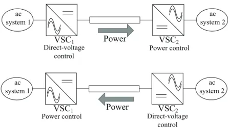
The typical configuration of a two-terminal VSC-HVDC system is displayed in Figure 2.1, where two VSCs are interconnected through a dc transmission line (cable or overhead trans-mission line). Usually, the control of the transmitted power flow over the dc-transtrans-mission line is achieved by setting one VSC to regulate the direct-voltage of the dc-node to which it is connected, and setting the other VSC to regulate the power. As will be explained later in
Figure 2.1: Two-terminal VSC-HVDC system.
Section 2.3, the control of the direct-voltage is essential for the operation of the VSC, since VSCs are able to generate a three-phase alternating-voltage with a desired phase, magni-tude and frequency as long as there is a sufficiently stiff direct-voltage source in the dc side
of the converter. The VSC’s ability of generating a desired alternating-voltage makes the independent control of the active and reactive power possible, which is one of the greatest advantages of this converter technology over the thyristor-based converters. Moreover, since the valves which compose the VSC allow bidirectional flow of current, the power can be reversed without the need of inverting the polarity of the direct-voltage, as opposite to the classical HVDC system. VSCs are suitable also for multi-terminal configurations, i.e. HVDC systems in which more than two VSCs are interconnected through a dc grid. Since the VSCs are essential devices of a VSC-HVDC system, the VSC station’s main components, operating principles and control system are described in the next sections.
2.2
Main components of a grid-connected VSC station
Figure 2.2 shows the typical configuration of a grid-connected two-level VSC station. Ty-pically, a VSC station is composed of capacitors in the dc side, and phase reactors, filters and transformers in the ac side. These components are briefly described next.
Figure 2.2: Configuration of a VSC station
2.2.1
DC side capacitor
The dc side capacitor is one of the key components of the VSC since it is this element which provides a stable direct-voltage from which the alternating-voltage can be generated. The capacitor also reduces the ripple introduced by the harmonics injected by the VSC into the dc side [15]. The capacitor rating is usually designed considering the amount of energy that the capacitor can store. Thecapacitor time constantis often used as a measure of the
amount of capacitor energy. Taking Figure 2.2 as a reference, the capacitor time constant is defined as
τ = Ce
2 1rated
whereCis the pole-to-neutral capacitance,e1rated is the pole-to-neutral rated voltage, and P1rated is the per-pole rated power of the VSC. Physically, the capacitor time constant
represents the time that it takes to fully discharge the capacitor when a constant power,
P1rated, is drawn from it. A τ of 2ms is recommended in [15], while in [10], it is claimed
that the total energy stored per rated power is typically 30-40kJ/MVA, which leads to a capacitor time constant of 30-40ms. In this thesis, 5ms is assumed. For example, from the values that will be indicated in Table 3.1 (e1rated = 300kV and P1rated = 300 MW
per-pole), the size of the capacitor is calculated as
C = 2(0.005)300
3002 (2.2)
which gives a capacitance of 33.33µF.
2.2.2
Phase reactor
The phase reactor facilitates the control of the active and reactive power exchange between the converter and the ac system. The voltage drop over the reactor induces a current whose phase and magnitude defines the power injected or absorbed by the converter. The VSC is able to generate an alternating-voltage with a desired phase angle and magnitude and, therefore, is able to control the current through the reactor via the voltage drop over it. The phase reactor also filters the high frequency harmonics of the current. Another function of the phase reactor is to limit short-circuit currents when faults occur in the dc side of the converter [15]. According to [15], the typical short-circuit impedance of this type of phase reactor is 0.15 pu.
2.2.3
AC side filters
As will be explained in the next section, the voltage generated by a VSC is composed of a fundamental frequency ac component, plus harmonics. These high-order harmonics are filtered through second or third-order high-pass filters, whose typical configurations are shown in Figure 2.3. Depending on the topology of the VSC, the high-order harmonic content can be decreased to a level where ac filters might be unnecessary.
2.2.4
Converter transformer
The main function of the converter transformer is to facilitate the interconnection of the VSC with an ac system of different rated voltage [15]. The transformer also isolates the ac grid from the multiples of the third-order harmonics and its multiples generated by the converter. Furthermore, the transformer provides galvanic isolation to the VSC station. The transformer typically has a tap-changer whose main function is to provide voltage regulation support to the system [15].
2.3
Operating principles
Different from line-commutated converters (classic HVDC), self-commutated converters
(VSC) are able to turn off their power electronic valves at any desired current flowing through them. This ability makes it possible that the VSC generates a desired alternating-voltage, provided it is connected to a sufficiently strong dc source on the dc side. As explained in this section, this makes it possible to control the active and reactive power independently, contrarily to the classical HVDC system. Later, the Pulse-Width Modu-lation (PWM) method is described. PWM is one of the most popular techniques used to generate alternating-voltage while avoiding low-order harmonics. Finally, the generation of alternating-voltages through multilevel topologies is briefly described
2.3.1
VSC as a controllable alternating-voltage source
Figure 2.4 shows the phase a of the valve bridge from Figure 2.2. Let us assume that a
strong dc source (instead of a capacitor) is connected to the dc side of the VSC. Then, consider the following sequence:
1. During the time∆t1,+Swais on, and−Swais off. Then,ucais+e1.
2. During the time∆t2,+Swais off, and−Swa is on. Then,ucais−e1.
The voltage uca generated by the previous sequence is as shown in Figure 2.4. A square
wave with two voltage levels, +e1 and−e1, is obtained, which is the reason why the
con-figuration shown in Figure 2.2 is called two-level converter.
The times ∆t1 and ∆t2 can be selected as desired, in such a way that a square wave of
50 Hz is generated with any phase angle. Moreover, considering that the direct-voltage source can change its magnitude, a square voltage with any phase angle and magnitude can be generated by the VSC. From the Fourier theory, the square wave is composed by a fundamental component plus harmonics, as
uca= (ˆuca)1sin(ω1t+φ1) +
∞
X
h=2
Figure 2.4: Phaseaof the valve arrangement (adapted from [8]).
where(ˆuca)1 is the amplitude of the fundamental sinusoidal component, ω1 is the
funda-mental frequency,φ1is the phase shift at the fundamental frequency,(ˆuca)his the amplitude
of theh-th harmonic,ωhis the angular frequency of theh-th harmonic, andφh is the phase
shift at theh-th harmonic frequency.
Considering only the fundamental component, waiving the need of filters, and the trans-former reactance included into the reactor impedance, the interconnection between the VSC and the ac system can be represented by the equivalent diagram shown in Figure 2.5. For such a system, it is well known that the steady-state active and the reactive power injected to the ac system are
Pg = uguc Xf sin(δ) (2.4) Qg =− u2g Xf +uguc Xf cos(δ) (2.5)
Considering that the angleδis very small1, thensin(δ)can be approximated toδandcos(δ) to 1. Equations (2.4) and (2.5) can be re-writen as
Pg = uguc Xf δ (2.6) Qg = uc−ug Xf ug (2.7)
From (2.6), it can be seen that the variation of theδproduces a larger variation ofPg, while
(2.7) shows that the variation of the voltage difference,uc−ug produces a larger variation
on the reactive power Qg. For that reason, it is usually claimed that the active power is
controlled by the angle difference of the voltages, and the reactive power is controlled by the magnitude difference of the voltages. Since the VSC can generate a voltage with any frequency, phase, and magnitude, then, the VSC is able to control the active and reactive power independently. Thus, VSCs can be seen as an ideal synchronous machine with no inertia. Different from synchronous generators, the VSC can adjust the phase angle of its generated voltage (and therefore the active power) in a very short time.
1The angle δis assumed to be around zero for the sake of illustration. Actually, for a VSC, δ could
Figure 2.5: AC side of the VSC, with the VSC represented by an ideal alternating-voltage source
Going back to Figure 2.4, the square waveform has a fundamental component with an amplitude equal to [9]
(ˆuca)1 =
4
πe1 (2.8)
and the amplitudes of the harmonics are (ˆuca)h =
(ˆuac)1
h , h= 3,5,7, ... (2.9)
Equation (2.9) shows that the low-order harmonics are relatively high, which is one of the disadvantages of this modulation method since filters for low order harmonics require bulky components. A solution to this are different modulation methods such as the sinusoidal pulse width modulation, the space vector modulation, or the harmonic elimination [9]. The pulse-width modulation method is summarized next.
2.3.2
Pulse-width modulation method
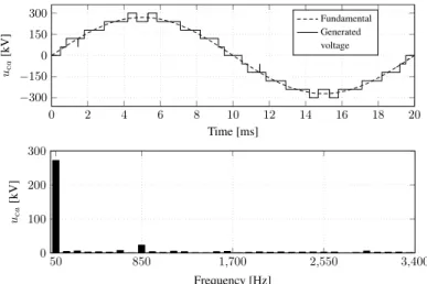
The Sinusoidal Pulse-Width Modulation (SPWM) method can be explained with the help of Figure 2.6. The SPWM defines the switching pattern for the VSC valves by comparing a carrier signal and a reference signal, as shown in Figure 2.6 (upper plot). In the example shown in the figure, the carrier signal is a 850 Hz triangular wave which varies from−1 to
+1. The reference signal is a 50 Hz sinusoidal waveform described as
urefa=masin(2πf1t+φ) (2.10)
where ma is called the amplitude modulation index, f1 is the frequency of the reference
voltage andφits phase angle. The signals are compared, and the following rule defines the
switching pattern:
1. If the reference is higher than the carrier, then+Swais on and−Swais off.
2. If the reference is lower than the carrier, then+Swa is off and−Swais on.
The resulting voltageuca(phase-to-neutral) is also shown in Figure 2.6 (middle plot),
con-sidering a rated direct-voltage of ± 300 kV and a amplitude modulation index of 0.9 (it
is also assumed ideal commutation for the valves). The harmonic spectrum in Figure 2.6 (lower plot), shows that the fundamental harmonic has a magnitude of 270 kV (0.9×300 kV). Moreover, the figure shows that there is considerable harmonic content at the multi-ples of the switching frequency, 850 Hz, and the side bands. It is shown in [9] that the three voltages generated by the converter using the PWM method state above are
Although the harmonic content is higher than the voltage generated by the square wave modulation, filtering high frequency harmonics requires smaller components which is con-venient to reduce costs and footprint. However, high switching frequency increases the
0 2 4 6 8 10 12 14 16 18 20 −1 0 1 Reference Carrier 0 2 4 6 8 10 12 14 16 18 20 −300 −150 0 150 300 Time [ms] uca [kV] Fundamental Generated voltage 50 850 1,700 2,550 3,400 0 100 200 300 Frequency [Hz] uca [kV]
Figure 2.6: Voltage generated by a two-level converter through the SPWM. Upper: Carrier and reference voltages. Middle: Voltage generated and fundamental component. Lower: Harmonic spectrum of the generated phase-to-neutral voltage.
switching losses in the VSC. The nature of the switching losses is described in [9], and it shown that they depend on the valve technology, the voltage across the valves, the current that the valves conduct, and the switching frequency. From that, the following are means to decrease the switching losses:
1. Decrease the switching frequency. However, that increases the low order harmonics which requires bigger filters. On the other hand, multilevel topologies decreases the individual switching frequency of the valves while improving the generated ac voltage waveform.
2. Decrease the voltage across the valves. That can be achieved through other VSC topologies such as the multilevel technology.
3. Improve the valve technology, in such a way that the switching process becomes faster.
Multilevel topologies have been proposed as a solution to improve the generated voltage waveform and to decrease the losses. With the multilevel technology, not only the voltage across the valves are decreased, but also the individual valve’s switching frequency, there-fore, the corresponding losses. A three-level Neutral-Point-Clamped (NPC) converter [8] is shown in Figure 2.7 and the generated voltage is shown in Figure 2.8. In contrast to the two-level converter, this type of converter allows three voltage levels,+e1,−e1 and0.
Moreover, in the two-level topology, the voltage across the valve is actually2e1, while in
this topology the voltage across the valves ise1. Furthermore, the harmonic content, shown
Figure 2.7: Three-level neutral-point-clamped converter 0 2 4 6 8 10 12 14 16 18 20 −300 −150 0 150 300 Time [ms] uca [kV] Fundamental Generated voltage 50 850 1,700 2,550 3,400 0 100 200 300 Frequency [kHz] uca [kV]
Figure 2.8: Voltage generated by a three-level converter through the SPWM. Upper: Voltage gene-rated and fundamental component. Lower: Harmonic spectrum of the voltage genegene-rated
A five-level NPC converter can also be constructed in the same way. Another topology is the flying-capacitor configuration, which can be reviewed in [8]. The more the number of levels, the less switching losses and the less the harmonic content. However, the main disadvantage is the complexity of the circuit, which increases with the number of levels. This is overcome by the recently developed multilevel topologies, which will be briefly described in Section 2.5.
2.4
VSC control system
Several control methods for the control of VSC have been developed and are available in the literature. For example, in the review carried out in [17], the resonant controller, the vector current control, and the power synchronization control methods are mentioned. The vector control method is widely used in grid connected VSCs [12,15] and it is the one used
in this thesis. The typical structure of a VSC control system is illustrated in Figure 2.9. The core of the control system is the Vector Current Controller (VCC), whose output is a three-phase voltage reference to the PWM block, which issues firing signals to the VSC switches. The VCC has two inputs,idfref andiqfref which are the current references.
Figure 2.9: VSC control system
Outer controllers are implemented in order to control other quantities, such as the active power, reactive power, voltage and alternating-voltage. The control of the direct-voltage involves active power, since the direct-direct-voltage value is defined by the amount of energy stored in the converter capacitor. Then, the referenceidfref is used to control either
the active power and the direct-voltage, as shown in the figure1. Another strategy can be to make the active power to be dependent on the direct-voltage, following a voltage-droop characteristic. The control of the alternating-voltage is related to the amount of reactive power support present in the system. Then, the referenceiqfref is used to control
either the reactive power or the alternating voltage. As in the dc side, the control of the alternating voltage can be done following a voltage-droop characteristic. A third strategy is to control the alternating-voltage to a fixed frequency waveform (working as a slack bus). This strategy is only useful when VSCs are connected to passive ac grids which do not count on ac sources (or they are weak).
In this section, the different blocks that integrate the control system of the VSC are de-scribed. The derivation of the VCC, which is implemented in thedqframe, is presented.
Furthermore, the phase-locked loop, which calculates the angle needed to perform thedq
transformation, is described. Afterwards, the derivation of the direct-voltage controller is presented. Finally, the active and reactive power controllers are described.
Since the description of the controllers involves voltages and currents in different
coordi-1It will be explained in the next section that thedqframe is aligned to the rotating voltage vectoruαβ g .
nate systems, the conventions and symbols adopted in this thesis are as specified in Appen-dix B. Moreover, in most of the cases, the electrical variables are expressed in per-unit values, whose base definitions are also presented in Appendix B.
2.4.1
Vector current control method
The principle of the vector current control method lies in finding the right magnitude and phase of the generated voltage, in such a way that the induced current over the phase reactor has the desired phase and magnitude. In the vector current control method implemented in a rotating frame1, the three-phase ac quantities are transformed to two dc quantities through the so-called dq transformation which is detailed in Appendix A. As an illustration, in
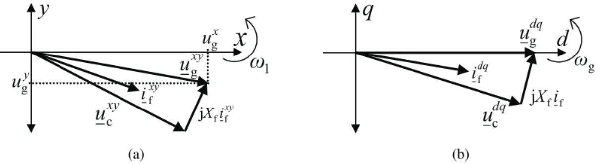
Figure 2.10, the steady-state vector diagram of the voltage drop over the reactor and the corresponding current is plot in two coordinate systems. In Figure 2.10(a), vectors in a generic rotating frame, the xy frame, are shown. Thexy frame it is a coordinate system
which rotates at the same speed than the vectors, but not aligned to any of them. The vector
uxyg , in thexyframe, is expressed as
uxyg =uxg + juyg. (2.12)
From the vector diagram in thexyframe shown in Figure 2.10(a), the complex powerSgis
calculated as
Sg =Pg + jQg =uxyg (ixyf )∗ (2.13)
from where, the active power and reactive power are
Pg = uxgixf +uygi
y
f (2.14)
Qg =−uxgify +uygixf. (2.15)
On the other hand, Figure 2.10(b) shows the mentioned steady-state vector diagram in the
dqframe where thedaxis is aligned to the vectorudqg . In that case, theqcomponent ofudqg
is zero. For instance, the vectorudqg , in thedqframe, is
udqg =udg. (2.16)
Then, applying (2.13) in thedqframe, the active and reactive power are
Pg = udgidf (2.17)
Qg =−udgi
q
f (2.18)
which means that the active power can be controlled with the dcomponent of the current,
idf, and the reactive power with theqof the current,iqf.
Considering the ac side of the system shown in Figure 2.11, the following equation, ex-pressed in theαβ frame (see Appendix B), describes the dynamics of the current through
the phase reactor.
diαβf dt =− Rf Lfi αβ f + 1 Lfu αβ g − 1 Lfu αβ c (2.19)
(a) (b)
Figure 2.10: Rotating reference frames. (a) genericxycoordinates not aligned toudqg . (b)dq
coor-dinates aligned toug.
Figure 2.11: Equivalent scheme of a VSC
Note that, in Figure 2.11, the VSC is represented as a voltage source in the ac side, and as a current source in the dc side. In thedqframe, (2.19) becomes
didqf dt =− Rf Lf idqf −jωgidqf + 1 Lf udqg − 1 Lf udqc (2.20) or more explicitly didf dt =− Rf Lfi d f +ωgiqf + 1 Lfu d g− 1 Lfu d c (2.21a) diqf dt =− Rf Lf iqf −ωgidf + 1 Lf uqg− 1 Lf uqc (2.21b)
where the synchronization angleθg (necessary to perform the dqtransformation) and the
frequencyωg are obtained from the three-phase voltageugby a Phase-Locked Loop (PLL).
From (2.21), it can be seen that there is a cross-coupling between the currents idf and iqf.
Moreover, it can be seen that the current idqf is affected by disturbances on the voltage udqg . If the current if and the voltageug are perfectly measured, the following control law
decouples the interaction betweenidf andiqf, and compensates the disturbances introduced
by variations on the voltageudqg
udqc ref =udqg −jωgLfidq +r. (2.22)
whereris the control input. Assuming that the VSC is ideal, then it can generate the output
voltage,udqc ref, exactly as requested by the VCC and with no delay, then
Considering (2.23), (2.22) can be entered to (2.20), resulting in di dt dq =−Rf Lf idq− 1 Lf r (2.24)
which is a decoupled, disturbance-free system. In [18], the internal model control method is used to design the VCC for electric drives applications, which has been further used in grid-connected VSC. Equation (2.24) can be expressed in the Laplace domain as
if =G(s)r (2.25) where if = idf iqf , G(s) = − 1 Lfs+Rf 0 0 −L 1 fs+Rf , r = rd rq (2.26) The inputrcan take the following form
r=F(s)(idqf ref −idqf ) (2.27) where F(s) = F(s) 0 0 F(s) , idqf ref = idfref iqfref (2.28) Equations (2.25) and (2.27) can be represented by the block diagram shown in Figure 2.12. From the figure, the closed-loop transfer function,Gc(s)is
Gc(s) = (I+G(s)F(s))−1G(s)F(s) (2.29) For the system (2.29) to be a decoupled first-order system, then, the following should be fulfilled G(s)F(s) = α s 0 0 αs (2.30)
Figure 2.12: Block diagram representation of (2.25) and (2.27)
whereαis the bandwidth of closed-loop system. Then,F(s)should be F(s) =G(s)−1 α s 0 0 αs = − αLf+ αRf s 0 0 − αLf+ αRsf (2.31) which means that F(s)is a proportional-integral (PI) controller with a proportional gain,
kp, equal to αLf and an integral gain,ki, equal to αRf. Finally, using (2.22), (2.27) and
(2.31), the control law is for the VCC in thedqframe is in time domain
udqc ref =udqg −jωgLfidqf −kp(idqf ref −i dq f )−ki Z t 0 (idqf ref −idqf )dt (2.32)
The output of the controller is the voltage referenceudqc ref, which is the input to the PWM
block as shown in Figure 2.9. As indicated by (2.11), the three-phase voltage generated by the converter, expressed in thedqframe is
udqc =udqc refe1 (2.33)
where, it must be stressed that udqc ref and e1 are in per unit. Equation (2.33) shows that,
even for ideal conditions, i.e. no delays and perfect measurement, the voltage generated by the VSC is not exactly the output of the VCC, but it depends on the dc-side direct-voltage. In order to avoid the influence of the direct-voltage, the voltage reference, udqc ref can be
pre-multiplied by 1
e1, as shown in Figure 2.13. In that case, the voltage generated by the
Figure 2.13: VCC representation in thedqframe
VSC will be equal to the voltage reference generated by the VCC, as
udqc =udqc ref. (2.34)
The VCC can be further improved with current limiters, anti-windup functions in case of voltage saturation, or active damping for disturbance rejection [20]. Other improvement is the operation under non-symmetrical conditions e.g. non-symmetrical faults, where al-gorithms to estimate the positive and negative sequence components of the current are proposed in [19,21]. These additional features, however, are not studied in this thesis since the small signal dynamics of the system is investigated in the neighborhood of an opera-ting point. Therefore, it is assumed that the converters are working in their linear range, unsaturated, and in balanced conditions only.
2.4.2
Phase-locked loop
The alignment of thedaxis to the rotating voltageuαβg is achieve by the knowledge of the
shown in Figure 2.14 and can be mathematically described as dnω
dt =kilε (2.35)
dθg
dt =nω+kplε (2.36)
wherenω is an state which accounts for the integral part of the PLL,θg is the phase angle
of uαβg , kpl and kil are gain parameters, and ε is the phase error. Equation (2.35) means
that the estimated frequency is updated with a term which is proportional to the error ε.
Furthermore, (2.36) says that the angle is updated by the integral of the estimated speed ˆ
ωg plus a correction factor which is proportional to the errorε [23]. The error, according
to [22], can have the form of
ε=KPLLsin(θgi −θg) (2.37)
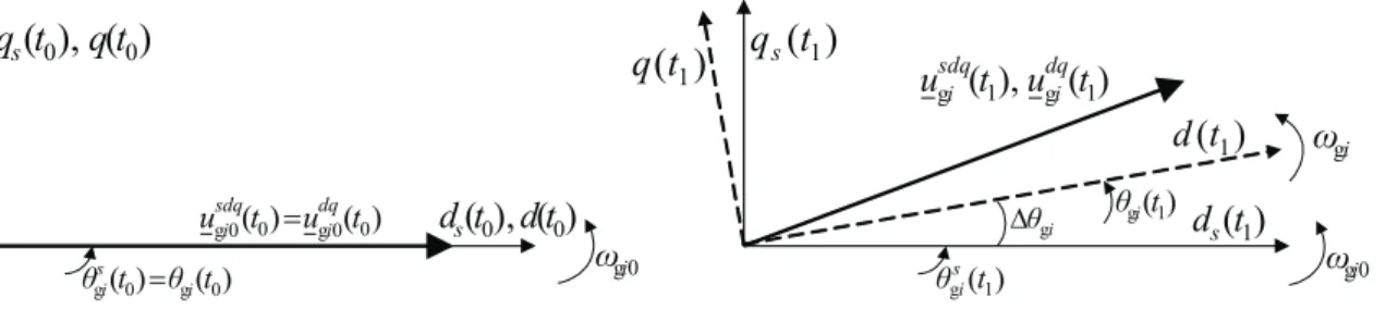
In Figure 2.15, a representation of theconverter dqframe1and theideally aligned dqframe2
are shown. The converter dqframe is not necessarily aligned to the vector uαβg , since the
Figure 2.14: Typical PLL block diagram.
PLL cannot estimate the correct angle instantaneously. On the other hand, the idealdq
frame is always aligned to the rotating voltageuαβg . The converterdqframe should be the
same as the idealdqframe in steady-state conditions, but not necessarily during a transient.
In Figure 2.15, thedaxis of the converterdqframe is intentionally not aligned, reflecting a
transient where the PLL is in the process of calculating the angle which alignsdaxis of the
converterdq frame to the rotating voltageuαβg . From the figure, it can be seen easily that
Figure 2.15: Comparison between the converterdqframe and ideally aligneddqframe.
theqcomponent of the voltage in the converterdqframe is given by
uqg =|uαβg |sin(˜θg) (2.38)
1In the converterdqframe, the angleθ
gestimated by the PLL is used to perform thedqtransformation. 2In the ideally aligneddqframe, thedaxis is always perfectly aligned to the rotating vectoruαβ
whereθ˜
g =θgi −θg. Equation (2.38) shows thatuqg can be used as the PLL error shown in
(2.37). IfKPLLin (2.37) is set to one, the normalized voltageuqg can be treated as the error
ε, that is ε= u q g |uαβg | (2.39) which is the expression used in [22] and [23]. In works such as [44–46], nevertheless, the per unit value ofuqg used as the input error of the PLL since they are used in grid-connected
VSCs. The error assumed in this thesis is then
ε =uqg (2.40)
and then, the block diagram shown in Figure 2.16 represents the PLL used in this thesis. Furthermore, the parameterskplandkilare selected as suggested in [18], that is
kpl= 2αPLL, kil =α2PLL (2.41)
whereαPLLis the bandwidth of the PLL. The value ofαPLLis a trade-off between a desired
speed of the PLL, and low-frequency harmonics and noise rejection [18, 24, 25]. In [24] a bandwidth of 5 Hz is selected, and in [23] it is mentioned a typical bandwidth of a PLL is between 3 and 5 Hz. In this thesis, a PLL bandwidth of 5 Hz is selected.
Figure 2.16: PLL block diagram implemented in this thesis.
2.4.3
Direct-voltage controller
The control of the direct-voltage provides the stiffness of a dc source from where the VSCs are able to generate the ac voltages. It also maintains the direct-voltage within acceptable limits. In works such as [45, 46], the energy stored in the VSC capacitor is controlled,
instead of the voltage e1 directly (See Figure 2.11). The expression that describes the
dynamics of the energy stored in the VSC (in per unit) is
C
2 de21
dt =P1−P12 (2.42)
whereP1 is the active power per-pole injected by the VSC to the capacitor, andP12is the
power that flows through the dc cable, as shown in the dc side of Figure 2.11. If the power
P1can be controlled perfectly, the following PI controller can be used to control the energy
of the VSC capacitor P1 =kpe (eref1 )2−e21 2 +kie Z t 0 (eref1 )2−e21 2 dt +P120 (2.43)
Figure 2.17: DVC block diagram
where the power P120 is the measurement of the power P12 which is feed-forwarded to
remove disturbances,kpe andkie are the proportional and the integral gains of the
Direct-Voltage Controller (DVC), and eref1 is the direct-voltage reference. Neglecting the losses
over the reactor and the VSC, the active powerP1 injected (or absorbed) by the VSC to the
capacitor can be approximated to the active power absorbed (or injected) from ac system at the node G (see Figure 2.11). Furthermore, If the VCC is assumed much faster than the DVC, the currentidf can be further approximated to the current referenceidfref. In that case
P1 ≈udgidfref. (2.44)
Hence, using (2.43) and (2.44), the control law of the DVC can be defined as
idfref = kpe ud g (eref1 )2−e21 2 + kie ud g Z t 0 (eref1 )2−e21 2 dt + P 0 12 ud g . (2.45)
If the powerP12 is measured perfectly, and assuming thatP1 is equal to (2.44), (2.45) can
be entered to (2.42) and the following can be obtained in the Laplace domain
e21 = C −1(k pes+kie) s2+C−1k pes+C−1kie (eref1 )2 (2.46)
whose characteristic polynomial is of second order and has the following form
s2+ 2ωnξs+ωn2 (2.47)
where ωn is the undamped resonance frequency, and ξ is the damping ratio. From (2.47)
the controller gains can be selected as
kpe = 2Cωnξ, kie =Cωn2 (2.48)
which are typical expressions that can be find in works such as [46, 54]. The design vari-ables are ωn andξ which has to be selected considering the assumption that the VCC is
much faster than the DVC.
Others authors, such as [21, 26], derive the DVC considering that the voltage e1 is
con-trolled, instead of the energy stored at the VSC capacitor. The following describes the dynamics of the voltage on the VSC capacitor
Cde1
wherei12is the current that flows through the dc cable as indicated in Figure 2.11.
Consi-dering the approximation made in (2.44), the currenti1 can be approximated as
i1 ≈
udgidfref
e1 (2.50)
then, the DVC is typically defined as the PI controller
idfref = e1 ud g kpe eref1 −e1 +kie Z t 0 eref1 −e1 dt +i012 . (2.51)
Using (2.49), (2.50) and (2.51), and considering thati012is equal toi12, a similar expression
as (2.46) is obtained e1 = C −1(k pes+kie) s2+C−1k pes+C−1kie eref1 . (2.52)
It must be highlighted that, under the considerations made, (2.46) and (2.52) are linear sys-tems which do not depend on the initial operating conditions1. The assumptions made are helpful to develop rules to select the controller parameters; however, when the assumptions are no longer considered, the system is actually nonlinear. The DVC which controls the energy of the VSC capacitor can be analyzed to show that. For instance, consider that the measurement P120 can be modelled as a low-pass filter of P12 and also that P12 is equal
e1i12. In addition, if aΠmodel is considered for the dc cable, the dynamics ofi12have to
be considered. Then, the state-space model of the VSC which control the direct-voltage is de21 dt =kpeC −1 (eref 1 )2−e21 +kieC−1n+ 2C−1P120 −2C−1e1i12 (2.53a) dn dt = (e ref 1 )2−e21. (2.53b) dP120 dt =−γP 0 12+γe1i12 (2.53c) di12 dt =− R12 L12i12+ 1 L12e1− 1 L12e2 (2.53d)
whereγis the bandwidth of device that measures the powerP12,naccounts for the integral
term of (2.45). In this model, the states aree21,n,P120 andi12, and the inputs areeref1 ande2.
Clearly, (2.53a) and (2.53c) are nonlinear since the terme1i12is the square root of the state
e21 multiplied by the statei12. The same can be deduced when (2.52) is analyzed.
Another controller can be implemented if the proportional and the integral terms, without feedforward term, of the DVC is directly fed to the current reference idfref without the
feedback linearizationperformed in (2.45) and (2.51). That is
idfref =kpe eref1 −e1 +kie Z t 0 eref1 −e1 dt (2.54)
which is going to be used in the analysis performed in Chapter 4 and 5 for the sake of simplicity.
2.4.4
Active cower control
The objective of the active power controller is to control the active power transfer over the VSC-HVDC system to the desired value. As mentioned in [21,26], the power controller can be implemented as a combination of an open-loop and feedback controller. The expression that defines the control law of the active power controller is
idfref = P ref g ud g +kpP Pgref −Pg+kiP Z t 0 Pgref −Pgdt. (2.55)
A block diagram representing (2.55) is shown in Figure 2.18. In this thesis, however, the active power is controlled directly with the current reference idfref without using the
controller shown in Figure 2.18.
Figure 2.18: Active power controller.
2.4.5
Reactive power and alternating-voltage control
Similarly to the active power controller, the reactive power controller can be implemented as a combination of an open-loop and a feedback controller, as follows
iqfref =−Q ref g uqg − kpQ Qrefg −Qg −kiQ Z t 0 Qrefg −Qg dt (2.56)
which, likewise, is represented in Figure 2.19. The alternating-voltage controller can be
implemented as a PI controller [26] iqfref =kpU urefg − |udqg | +kiU Z t 0 urefg − |udqg |dt. (2.57)
As assumed for the control of active power, the reactive power is controlled directly with the current referenceiqfref without using the controller shown in Figure 2.19
2.5
New challenges for VSC-HVDC systems
In recent years, VSC-HVDC systems have been in the spotlight, particularly, due to the development of new converter topologies, and the proposal of using VSCs in MTDC con-figurations. The developers of the new multilevel topologies claim to have reduced the losses of VSCs to a level similar to the thyristor-based HVDC systems. Moreover, VSCs are considered suitable for MTDC configuration due to their versatile controllability fea-tures. In this section, both topics are briefly reviewed.
2.5.1
New multilevel topologies
The Modular Multilevel Converter (MMC), the Cascaded Two-Level converter (CTL) and the hybrid-HVDC-circuit topology described in [10–12], overcomes the lack of modularity of the NPC topology previously introduced. The MMC and CTL, illustrated in Figure 2.20, are similar topologies which builds up the voltage uca by inserting the submodules
follo-wing a modulation method. The waveform generated by a twenty-module converter (ten modules in each arm) is shown in Figure 2.21. An eleven-level voltage is generated, and the harmonic spectrum shows that the harmonic level has decreased considerably compared to Figures 2.6 and 2.8. Apart from decreasing the harmonic content, the MMC reduces also the switching losses, since each submodule operates at lowers frequencies compared to the two and-three level converters. If the number of submodules is increased1, the generated voltage waveform can be almost sinusoidal, so filters might become significantly small or even unnecessary.
The hybrid-HVDC-circuit configuration is described in [12]. It consist of a series con-nection of a two-level configuration and a H-bridge modules as illustrated in Figure 2.22. Basically, the idea is to use the two-level part of the converter to generate a low frequency voltage waveform and to use the H-bridges as active filter to shape the ac voltage wave-form [13]. The main advantage of this topology compared to the MMC and CTL topologies is its performance in dc side faults. In case of dc side faults, the valves of the H-bridges will turn off in such a way that the converter stops feeding the fault. In the case of the MMC and CTL, a dc side fault will be fed through the diodes connected in anti-parallel with the valves.
Figure 2.20: Modular Multilevel Converter [11].
2.5.2
VSC-based multi-terminal HVDC systems
An MTDC system can be defined as an HVDC system where more than two VSCs are interconnected through a common dc grid. Similarly to ac systems, in an MTDC system there might be a number of converters injecting power into the dc grid (analogously to generators in ac systems) and a number of converters absorbing power from the dc grid (analogously to loads in ac systems). Furthermore, some converters can be operated in vol-tage regulating mode, similar to the frequency-regulating generators that are operated in ac systems, i.e. compensating the unexpected “generation-load” mismatches. In that regard, it has been recognized in [30] that the control of the direct-voltage plays an important role on the power balancing task of the dc side. The following are the main conclusions from [30]: 1. Power unbalances in the dc system produces fluctuations in the direct-voltage of the system. If there is excess (deficit) of power going into the dc system, the direct-voltage will increase (decrease). Then, the direct-direct-voltage can be used as an indicator of power unbalances in the dc side, as the frequency is used in the ac side.
2. The VSC which controls the direct-voltage acts as the slack generator in ac systems. It compensates the deficit or surplus of the power in the MTDC system.
3. The dynamics of the dc side is fast since capacitors are designed to store only a small amount of energy. Then, measures to compensate power unbalances should be taken automatically.
Using those principles, control strategies have been proposed in works such as [31–33]. The control strategies in the dc side aim at providing a back up to the direct-voltage control in case of contingencies such as faults in the ac side, or converter outages. The most basic control strategy in an MTDC is that one single VSC controls the direct-voltage while the
0 2 4 6 8 10 12 14 16 18 20 −300 −150 0 150 300 Time [ms] uca [kV] Fundamental Generated voltage 50 850 1,700 2,550 3,400 0 100 200 300 Frequency [Hz] uca [kV]
Figure 2.21: Voltage generated by a 20 module MMC through the SPWM. Upper: Generated tage and fundamental component. Lower: Harmonic spectrum of the generated vol-tage.
Figure 2.22: Hybrid-HVDC-circuit topology [12].
others control their power set-points to a fixed value. However, the disadvantage of such control strategy is that, if there is an outage of the only VSC which controls the direct-voltage, the voltages will either rise or drop in the dc system in a sustained way.
In Figure 2.23, a three-terminal HVDC system is shown. The system is composed of the VSC1, VSC2and VSC3, whose voltages at their dc side nodes aree1,e2ande3, respectively.
Moreover, the VSC1, VSC2 and VSC3 transfer the powers P1, P2 and P3 to the dc grid,
where a positive value means that the converter “supplies” power to the dc grid, while a negative value means the converter “consumes” power from the dc grid. This setup is used to explain the voltage-margin control and the voltage-droop control strategies.
The voltage-margin control strategy has been presented in [31, 32]. As an example, in Figure 2.24, the voltage-power characteristic of each VSC (in the system from Figure 2.23) would follow under the voltage-margin control strategy. According to Figure 2.24, VSC1
Figure 2.23: Three-terminal HVDC system.
(assuming a lossless dc grid). According to the voltage-margin control, if the converter VSC1 is lost, VSC2 and VSC3will continue supplying 300 MW together. As stated earlier
in this section, this surplus of power will make the voltage of the dc grid to increase. From the figure, it can be seen that VSC3 will change from a constant power control mode to a
direct-voltage control mode when the voltage at its dc-node increases toe03. Finally, after
the outage of VSC1, VSC2 will be supplying 100 MW, and VSC3 will be consuming 100
MW and will be controlling the direct-voltage of the system.
Figure 2.24: Voltage-margin control strategy withe01< e03< e02.
The disadvantage of this method is that, only one converter is exposed to large variations of power in case of contingencies. In our example, VSC3 has to change from+100 MW
to −200 MW which means that a fast variation of a 300 MW will be experienced in the VSC3’s ac side.
In order to overcome the disadvantage of the voltage-margin control, the voltage droop-control is proposed in [33, 34]. A voltage-droop droop-control strategy for the studied three-terminal HVDC system is shown in Figure 2.25. In this scheme, if VSC1 is suddenly out
of service, the voltage will rise in the dc system, and the power output of VSC2 and VSC3
will change according to the voltage-power characteristics shown in Figure 2.25 the voltage will rise until the power in the dc-system is balanced. The advantage of this method is that, the balance of the power is performed by the two remaining converters instead of only one. However, the disadvantage is that the final power set-points are uncontrolled. One method to control the power after the contingency is proposed in [57]. In Figure 2.26 the principle of the method is illustrated. Basically, the power can be controlled by changing theno-load voltageof the voltage-droop characteristic. For instance, if the power output of
Figure 2.25: Voltage-droop control strategy.
a converter is−300 MW after the contingency, it can be changed to−100 MW (if desired) by increasing the no-load voltage value of voltage-droop characteristic.
Figure 2.26: Autonomous power control.
Through solving the problem of the power balance in the dc side of an MTDC system, some control strategies have been proposed. However, an MTDC is a system which is composed of complex elements such as the VSC and the dc grid. The dynamics of a VSC, for example, depends on the control structure which, likewise, has to do with the selection of the control strategies proposed in this section. The dc grid on the other hand, is composed by cables and overhead transmission lines, which shows a resonance behaviour in certain conditions. Then, along with considering the power balance issue, the dynamic interactions between elements that conform the MTDC have to be studied when developing a control strategy for MTDC systems.
2.6
Conclusions
In this Chapter, a basic theory on VSC-HVDC systems has been presented. The functions of the main components of a VSC, together with their typical ratings has been summa-rized. The operating principles of the VSC have been presented and the SPWM modula-tion method has been introduced. Then, a typical control system of the VSC has been de-scribed with a special stress on the derivation of the vector current controller and the direct-voltage controller, and the selection of their parameters. Finally, the new challenges for VSC-HVDC system, regarding new converter topologies and the control of multi-terminal HVDC systems, have been presented.
Overview on dc network dynamics
Considerable research effort on the subject of control and stability of dc networks can be found in the literature [31–38,49,50,52]. On a low power level, it has been recognized that constant power loads (CPLs) in dc microgrids introduce an incremental negative resistance, which can be detrimental for the dynamic performance of the system. Various analysis methods and control strategies have been proposed to overcome the instability introduced by CPLs. On the high power level, several works have been carried out concerning the stability of HVDC systems, however, with emphasis on the ac side dynamics rather than the dc side of the system. The interest on the dc side dynamics has risen when MTDC systems have come into the scene, since the conditions in MTDC are more variable than in point-to-point HVDC systems. The small signal analysis has been used, mostly to assess the effect of the operating conditions and the controller parameters on the stability of the studied MTDC systems.
In order to get an idea of the challenges that brings HVDC systems from the dynamics perspective, a review of publications on the dynamic analysis of dc microgrids and HVDC systems has been carried out. The main findings from the review are presented in this chapter.
3.1
Dynamic issues in dc microgrids
Multi-converter power electronic systems, in the form of dc microgrids, have been a sub-ject of research for some years. In [36], for instance, definitions and applications of multi-converter power electronics systems are presented. Proposed dc microgrids configurations for automotive power systems, electric and hybrid vehicles, aircraft power systems, and space power systems are presented as examples. As shown in Figure 3.1, a dc microgrid is typically composed of a number of converters connected to a common bus. Those con-verters interface either power sources or loads or can be used to interconnect systems of different voltage levels. From the dynamic point of view, the challenges in multi-converter systems, as stated in [36], ranges from system modelling, dynamic assessment and control.
![Figure 2.4: Phase a of the valve arrangement (adapted from [8]).](https://thumb-us.123doks.com/thumbv2/123dok_us/10180289.2920433/27.892.237.741.146.332/figure-phase-valve-arrangement-adapted.webp)
![Figure 2.7: Three-level neutral-point-clamped converter 0 2 4 6 8 10 12 14 16 18 20−300−1500150300 Time [ms]uca[kV] FundamentalGeneratedvoltage 50 850 1,700 2,550 3,4000100200300 Frequency [kHz]uca[kV]](https://thumb-us.123doks.com/thumbv2/123dok_us/10180289.2920433/30.892.222.599.141.416/figure-level-neutral-point-clamped-converter-fundamentalgeneratedvoltage-frequency.webp)
![Figure 2.20: Modular Multilevel Converter [11].](https://thumb-us.123doks.com/thumbv2/123dok_us/10180289.2920433/42.892.203.622.132.481/figure-modular-multilevel-converter.webp)
![Figure 3.6: Stability criteria [40]. (a) Middlebrook criterion. (b) Gain margin phase margin crite- crite-rion](https://thumb-us.123doks.com/thumbv2/123dok_us/10180289.2920433/50.892.122.709.895.1096/figure-stability-criteria-middlebrook-criterion-gain-margin-margin.webp)
![Figure 3.9: One simplified model of a VSC [48].](https://thumb-us.123doks.com/thumbv2/123dok_us/10180289.2920433/54.892.102.730.141.353/figure-simplified-model-vsc.webp)