MEMRISTOR: MODELING, SIMULATION AND
USAGE IN NEUROMORPHIC COMPUTATION
by
Miao Hu
M.S. in Electrical Engineering,
Polytechnic Institute of New York University, 2011
Submitted to the Graduate Faculty of
the Swanson School of Engineering in partial fulfillment
of the requirements for the degree of
Doctor of Philosophy
University of Pittsburgh
2014
UNIVERSITY OF PITTSBURGH
SWANSON SCHOOL OF ENGINEERING
This dissertation was presented
by
Miao Hu
It was defended on
June 9th, 2014
and approved by
Hai Li, Ph.D., Assistant Professor, Department of Electrical and Computer Engineering
Luis F. Chaparro, Ph.D., Associate Professor Emeritus, Department of Electrical and
Computer Engineering
Yiran Chen, Ph.D., Associate Professor, Department of Electrical and Computer
Engineering
William E. Stanchina, Ph.D., Chairman and Professor, Department of Electrical and
Computer Engineering
Qing Wu, Ph.D., Air Force Research Lab
Dissertation Director: Hai Li, Ph.D., Assistant Professor, Department of Electrical and
Copyright c by Miao Hu 2014
MEMRISTOR: MODELING, SIMULATION AND USAGE IN NEUROMORPHIC COMPUTATION
Miao Hu, PhD
University of Pittsburgh, 2014
Memristor, the fourth passive circuit element, has attracted increased attention from vari-ous areas since the first real device was discovered in 2008. Its distinctive characteristic to record the historic profile of the voltage/current through itself creates great potential in fu-ture circuit design. Inspired by its high scalability, ultra low power consumption and similar functionality to biology synapse, using memristor to build high density, high power efficiency neuromorphic circuits becomes one of most promising and also challenging applications. The challenges can be concluded into three levels: First, at device level, memristors as emerg-ing nano devices greatly suffer from process variations. Some materials also demonstrate stochastic switching behavior. All these impacts should be considered and efficiently mod-eled. Considering that memristor devices can be realized in different memristive materials, a general modeling method of process variations and stochastic switching behavior that is independent with device’s physical models is preferred; Second, at circuit level, cross-point array fabrication is usually employed in realizing high density memristive circuits. How-ever, current cross-point simulation is either not accurate enough or not efficient for large scale simulation, like 1024×1024 array. An efficient and flexible cross-point array simulation platform is necessary to explore the performance of memristive cross-point arrays in neuro-morphic computation; Third, at application level, how to apply and evaluate the emerging memristor in neuromorphic circuit design is unclear. Many modification need to be carried out in neural network algorithms and circuit realizations to take memristor’s advantages as well as alleviate its shortages. Generally, although memristor is widely accepted as one of
the most important keys for future high efficient, low power computation, how to design high performance realistic memristive neuromorphic circuits remains a open question, which is the major study topic in this thesis.
At device level, I designed a series of models for general memristors to study the impact of process variations and stochastic behavior on memristor device and memristive circuits. First I analyzed the impact of the geometry variations on the electrical properties of TiO2 -based memristors, including line edge roughness (LER) and thickness fluctuations (TF). A simple algorithm was proposed to generate a large volume of geometry variation-aware three-dimensional device structures for Monte-Carlo simulations. Then a statistical model is extracted accordingly. Simulations show that the statistical model is 3∼4 magnitude faster than the Monte-Carlo simulation method, with only∼2% accuracy degradation. In addition, the stochastic switching behaviors have been widely observed in metal oxide memristors. To facilitate the investigation on memristor-based hardware implementation, we built a stochas-tic behavior model of TiO2 memristive devices based on the real experimental results. These models could be extended to general memristors to study the impact of process variations and stochastic behavior on memristor operations.
At circuit level, I integrated a full set of device models and variation models into the point array structure to evaluate its performance. By efficiently formulating the entire cross-point array, the simulator is 2∼3 orders of magnitude faster than traditional SPICE simulator without accuracy degradation. In this way, designers could look into the memristive cross-point array with scale and accuracy which has never been achieved before. The results firstly show how sneaking current leakage map changes in crossbar arrays, and quantitatively evaluate the impact of circuit, device and variation parameters. This simulator paves the road for further application-level studies.
At application level, I focused our study on memristor-based neuromorphic circuits with the models and tools developed in front. I first proposed a few low power neuromorphic components with memristors, including based synapse “macro cell”, memristor-based stochastic neuron and memristor-memristor-based spatio-temporal(MST) synapse. These designs employee memristors to achieve ultra high power efficiency, and have high tolerance to pro-cess variations and stochastic behaviours. In addition, all these components are friendly to
cross-point array integration so they could be applied to large scale neuromorphic circuit applications.
I also extended my study to large scale neuromorphic circuit for artificial neural network (ANN) applications. In one work, I explore the potential of a memristor crossbar array that functions as an auto-associative memory and apply it to Brain-State-in-a-Box (BSB) neural networks, which belongs to traditional neural networks for spatial pattern recognition. More specifically, the recall and training functions of a multi-answer character recognition process based on BSB model are studied. The robustness of the BSB circuit is analyzed and evaluated based on extensive Monte-Carlo simulations, considering input defects, process variations, and electrical fluctuations. The results show that the hardware-based training scheme proposed in the work can alleviate and even cancel out majority of the noise issue. In another work, I further studied the memristor-based hardware realization of spiking neural network (SNN) for temporal pattern learning, which is the third generation and also the latest generation of neural networks. A temporal pattern learning application is applied to evaluate the performance of MST synapses in neural networks. The learning ability when utilizing STDP and ReSuMe learning rules were examined. The simulation results show that MST synapses can realize online spike-timing-based learning at nano-second scale with an average energy consumption of 36.7pJ and 64.0pJ per spike for STDP and ReSuMe learning rules, respectively. The energy consumption in recall process is only 14.6pJ per spike. The simple design structure, enhanced functionality, fast execution, and high energy efficiency of MST synapses potentially lead to highly scalable neuromorphic hardware designs.
In conclusion, in this thesis I introduce a complete hardware design flow of memristor-based neuromorphic circuits from device level to application level. The impact of variation-s, device parameters and circuit operation schemes are studied at different levels to give a accurate and complete evaluation of memristors’ performance in neuromorphic circuits. Moreover, a series of modifications and designs at different levels are also carried out to optimize the performance of memristor-based neuromorphic circuits. Our result shows that memristor-based neuromorphic computation could be ∼ 2orders of magnitude power effi-cient than traditional CMOS computation, and is an ideal platform for “brain-like” high performance computation.
TABLE OF CONTENTS
1.0 INTRODUCTION . . . 1
1.1 Motivation . . . 1
1.1.1 Device to device variation . . . 3
1.1.2 Device controllability and stochastic behaviour . . . 4
1.1.3 Large scale cross-point array analysis . . . 5
1.1.4 Circuit performance analysis base on applications . . . 5
1.2 Contributions . . . 6
1.2.1 Memristor variation model . . . 7
1.2.2 Memristor stochastic model . . . 7
1.2.3 Efficient memristor cross-point array simulator . . . 7
1.2.4 Memristor-based neuromorphic circuit components . . . 8
1.2.5 Memristor-based neurmorphic circuit for spatial pattern recognition . 9 1.2.6 Memristor-based spiking neurmorphic circuit for temporal pattern recog-nition . . . 10 1.3 Thesis roadmap. . . 11 2.0 PRELIMINARY . . . 12 2.1 Memristor . . . 12 2.1.1 Theoretical memristors . . . 12 2.1.2 Memristor devices . . . 13
2.1.2.1 TiO2 thin-film memristor . . . 13
2.1.2.2 Spintronic memristor . . . 14
2.2 Synapse theory . . . 17
2.2.1 Biological Synapse . . . 17
2.2.2 Artificial Neural Network (ANN) Synapse . . . 18
2.2.3 Electronic Synapse. . . 19
2.3 Neural network . . . 21
2.3.1 Brain-state-in-a-Box neural network for spatial learning . . . 21
2.3.2 Spiking neural network for temporal learning . . . 23
3.0 MEMRISTOR MODELS FOR CIRCUIT SIMULATION . . . 26
3.1 Memristor variation model. . . 26
3.1.1 Mathematical analysis. . . 26
3.1.1.1 TiO2 thin-film memristor . . . 26
3.1.1.2 Spintronic memristor . . . 30
3.1.2 3D memristor structure modeling . . . 32
3.1.3 Experimental results. . . 35
3.1.3.1 Simulation setup . . . 35
3.1.3.2 TiO2 thin-film memristor . . . 36
3.1.3.3 Spintronic memristor . . . 38
3.1.4 Similarities and differences . . . 40
3.1.5 Conclusion . . . 41
3.2 Statistical memristor model . . . 42
3.2.1 Statistical analysis of memristor model . . . 42
3.2.1.1 Distribution of R0H and R0L . . . 42
3.2.1.2 Distribution of
ω
0 . . . 433.2.1.3 Distribution of M0 . . . 47
3.2.2 Model generation flow . . . 47
3.2.3 Simulation results . . . 49
3.3 Stochastic memristor model . . . 53
3.3.1 On and OFF Static States . . . 53
3.3.2 Dynamic Switching Process . . . 54
3.4 Summary . . . 60
4.0 EFFICIENT SIMULATOR FOR MEMRISTIVE CROSS-POINT AR-RAY SIMULATION . . . 61
4.1 MATLAB-based simulation overflow . . . 61
4.2 Simulation setup . . . 62
4.2.1 Cross-point array model. . . 63
4.2.2 Memristor model . . . 64
4.2.3 Selector model . . . 65
4.2.4 Variation model . . . 66
4.2.4.1 Cycle-to-cycle variation model . . . 66
4.2.4.2 Device-to-device variation model . . . 68
4.3 Accuracy and efficiency evaluation . . . 68
4.4 Summary . . . 70
5.0 MEMRISTOR-BASED NEUROMORPHIC CIRCUIT COMPONENTS 71 5.1 “Marco cell” for high-definition weight storage . . . 71
5.1.1 Characterization of multiple memristive switches . . . 71
5.1.2 “Marco cell” design . . . 72
5.1.3 Feedback attempt scheme . . . 74
5.2 Memristor-based stochastic neuron . . . 75
5.2.1 Binary stochastic neuron . . . 78
5.2.2 Continuous value stochastic neuron . . . 78
5.3 Memristor-based spatio-temporal(MST) synapse . . . 80
5.3.1 Design concept . . . 80
5.3.2 MST synapse characterization . . . 82
5.3.2.1 DC Response . . . 83
5.3.2.2 Response to Spiking Excitation . . . 83
5.3.3 Synaptic properties of MST synapse . . . 84
5.3.3.1 Spike-timing-based recall . . . 84
5.3.3.2 Weight tunability . . . 86
5.4 Summary . . . 89
6.0 MEMRISTOR-BASED ANALOG NEUROMOPHIC CIRCUITS . . . 90
6.1 Design methodology . . . 90
6.1.1 Mapping a connection matrix to a cross-point array . . . 90
6.1.1.1 Cross-point array vs. matrix . . . 90
6.1.1.2 A fast approximation mapping function . . . 92
6.1.1.3 Transformation of BSB Recall Matrix . . . 93
6.1.2 Training memristor cross-point arrays in BSB model . . . 94
6.2 Hardware design and robustness analysis . . . 95
6.2.1 BSB recall circuit . . . 95
6.2.2 BSB training circuit . . . 98
6.3 Robustness of BSB Recall Circuit . . . 101
6.3.1 Process variations . . . 101
6.3.1.1 Memristor cross-point arrays . . . 101
6.3.1.2 Sensing Resistance . . . 102
6.3.2 Signal fluctuations . . . 102
6.3.3 Physical challenges . . . 103
6.3.4 Impact of sneak paths . . . 103
6.4 Simulation results I - Recall . . . 104
6.4.1 BSB circuit under ideal condition . . . 104
6.4.2 Process variations and signal fluctuations . . . 106
6.4.3 Impact of summing amplifier resolution . . . 108
6.4.4 Overall performance . . . 111
6.5 Simulation result II - Training. . . 112
6.5.1 Convergence speed analysis . . . 113
6.5.2 BSB circuit as auto-associative memory . . . 115
6.5.3 Nonlinear memristance change . . . 118
6.5.4 Defected cells . . . 119
7.0 MEMRISTOR-BASED SPIKING NEUROMORPHIC CIRCUITS FOR
TEMPORAL LEARNING . . . 123
7.1 MST synapse for temporal learning . . . 123
7.1.1 STDP Learning Rule . . . 123
7.1.2 ReSuMe Learning Rule . . . 125
7.1.3 “The 1st Spike Dominates” property . . . 128
7.2 MST synapse-based spiking neuromorphic circuits for temporal pattern recog-nition . . . 129
7.2.1 Application Setup . . . 129
7.2.2 Learning Temporal Patterns using STDP . . . 130
7.2.3 Learning Temporal Patterns using ReSuMe . . . 130
7.2.4 Energy Estimation . . . 131
8.0 CONCLUSION AND FUTURE WORKS . . . 133
LIST OF TABLES
1 The Device Dimensions of Memristors.. . . 26
2 The Parameters/Constraints In LER Characterization. . . 34
3 Memristor Devices and Electrical Parameters . . . 36
4 3σ min./max. of TiO2 memristor parameters . . . 40
5 3σ min./max. of spintronic memristor parameters . . . 41
6 Statistical model of TiO2 thin-film memristor.. . . 47
7 Statistical model parameters . . . 50
8 Variance between 3D model and statistical model. . . 50
9 PF(%) of 26 BSB circuits for 26 input patterns. . . 107
LIST OF FIGURES
1 Comparison of traditional approach with MST synapse approach. . . 9 2 TiO2 thin-film memristor. (a) structure, and (b) equivalent circuit. . . 13
3 TMR-based spintronic memristor. (a) structure, and (b) equivalent circuit. . 15 4 A simple example of neural network. . . 20 5 BSB training algorithm using Delta rule. . . 22 6 A spike-timing-based model for spatio-temporal pattern recognition. (a) The
overview of the spike-timing-based model for vision system; (b) A general LPE flow; (c) An example of spatio-temporal pattern conversion: the image “5” is partitioned and converted to multiple spike-timing trains. . . 23 7 Spike-timing-based learning rules and diagrams of neuron connections. (a)
STDP learning rule; (b) ReSuMe learning rule. . . 24 8 An example of 3D TiO2 memristor structure, which is partitioned into many
filaments in statistical analysis. . . 27 9 An example of 3D TMR-based spintronic memristor structure, which is
parti-tioned into many filaments in statistical analysis. . . 30 10 The flow of 3D memristor structure generation including geometry variations. 32 11 LER characteristic parameters distribution among 1000 Monte-Carlo
simula-tions. Constraints are shown in red rectangles. . . 35 12 Simulation results for TiO2 thin-film memristors. The blue curves are from
100 Monte-Carlo simulations, and red lines are the ideal condition. From top left to right bottom, the figures areRH vs. RL; M(t) vs. t; v vs. ω; ω vs. t;
13 Simulation results for spintronic memristors. The blue curves are from 100 Monte-Carlo simulations, and red lines are the ideal condition. From top left to right bottom, the figures areRH vs. RL; M(t) vs. t; v vs. ω; ω vs. t; I
vs. t; and I−V characteristics. . . 39
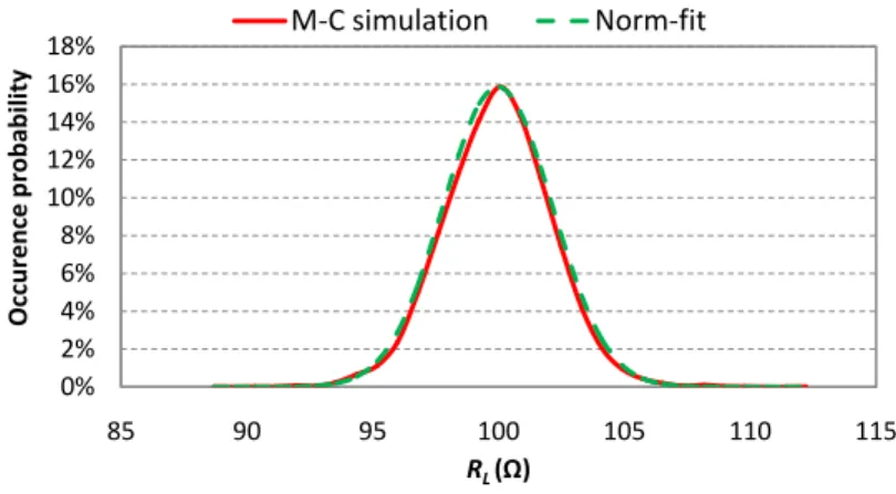
14 The Distribution of R0L from 10,000 Monte-Carlo simulations and the fitting curve of Eq. (3.25). . . 43
15 ±3σ variances of ω vs. Vap att = 1s. . . 45
16 ω0(t) whenVap = 1.1V based on 100 Monte-Carlo simulations. . . 45
17 Comparison ofω0(t) at ±3σ corners. . . 51
18 Comparison ofM0(t) at ±3σ corners. . . 51
19 Comparison ofI−V at ±3σ corners. . . 51
20 ±3σ variances of M vs. f att= 21f. . . 52
21 ±3σ variances of M vs. Vap at t= 1s. . . 52
22 The static state distribution of a TiO2 memristor device. . . 57
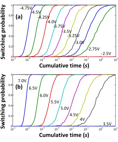
23 The time dependency of ON (a) and OFF (b) switching at different external voltageV. . . 58
24 The analog switching process of a TiO2 memristor. . . 59
25 Matlab simulation flow . . . 62
26 Memristor crossbar model . . . 63
27 I-V curve of TaOx memristor device compact model . . . 64
28 I-V curve of selector model based on TiN tunnelling device, the fitting error at high voltage probably comes from the compliance current limitation. . . . 65
29 I-V curve of Nonlinear device with TaOx memristor in series connection with the TiN selector. . . 66
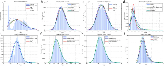
30 Distribution of HRS/LRS from the 2 billion on/off cycles of single TaOx device. a,e are the overall resistance distribution for HRS and LRS, respectively. b,c,d and f,h,i stand for the first billion cycles, next 0.5 billion cycles and the last 0.5 billion cycles for HRS and LRS, respectively. . . 67
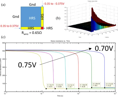
31 Simulation examples. (a) Simulation setup; (b) Static simulation result of volt-age map for 64-by-64 linear cross-point array; (c) Dynamic simulation result
of voltage on selected device for 4-by-4 linear cross-point array. . . 69
32 Simulation speed of linear cross-point array with different size. . . 70
33 The conductance distribution of parallel connected memristive switches. . . . 72
34 (a) A macro cell containing of 9 memristive switches on a 3x3 crossbar. (b) Partitioning a 6x6 memristive switch crossbar to obtain a 2x2 macro cell cross-bar for continuous weight storage. . . 73
35 Average (a) and Worst-case (b) reconfiguration cycles to reach target conduc-tance with different absolute errorE. . . 75
36 Binary/Continuous value stochastic neuron design . . . 76
37 Output example of binary stochastic neuron. . . 76
38 Voltage dependency of ON (a) and OFF (b) switching at different pulse widths tswitch . . . 77
39 Output example of binary stochastic neuron. . . 79
40 Voltage dependency of ON (a) and OFF (b) switching at different pulse widths tswitch . . . 79
41 MST synapse design and I-V characteristics. (a) MST structure and equivalent circuit; (b) Conceptual layout in cross-point array; (c) DC-sweep I-V curves of the MST synapse, M1, and M2 when applying a small voltage (top figures) or a large voltage (bottom figure). . . 81
42 The I-V curve of a TaOx device. Reproduced based on Strachan et al. (2013). 82 43 The state transition diagram of MST synapse under spiking excitations. . . . 83
44 MST synapse in spike-timing-based recall – Case 1. . . 85
45 MST synapse in spike-timing-based recall – Case 2. . . 85
46 MST synapse in spike-timing-based recall – Case 3. . . 85
47 The tunability of MST synapse. . . 87
48 Resistance ratio between M1 and M2. Gray area is the working region that satisfies Eq. (5.2). . . 88
50 The conceptual diagram of the BSB recall circuit. . . 96
51 Embedded BSB training circuit: (a) training flow; (b) conceptual circuit dia-gram; (c) error detection circuit. . . 99
52 (a) Random line defects; (b) Random point defects. . . 104
53 Simulation setup of BSB recall circuit. . . 105
54 Iterations of 26 BSB circuits for a perfect “a” image. . . 105
55 The ideal performance of 26 BSB circuits . . . 106
56 Static noise vs. dynamic noise. . . 107
57 The impact of CorrM. . . 109
58 Impact of resolutions of summing amplifiers. . . 110
59 PF for each character pattern . . . 111
60 Experiment 1: Iteration number vs. magnitude summation of output voltage signals. . . 113
61 Experiment 2: Iteration number vs. magnitude summation of output voltage signals. . . 114
62 Experiment 3: Error correction rate. . . 117
63 Experiment 3: Uniform size of domain of attraction. . . 117
64 Experiment 3: Quality of Domain of attraction. . . 117
65 Error correction rate. (a) LRS/LRS, G1=30; (b) LRS/HRS, G1=30; (c) HRS/HRS, G1=30; (d) HRS/HRS, G1=50; (e) HRS/HRS, G1=50, defected cells are only in diagonal direction. . . 120
66 Uniform size of domain of attraction. (a) LRS/LRS, G1=30; (b) LRS/HRS, G1=30; (c) HRS/HRS,G1=30; (d) HRS/HRS,G1=50; (e) HRS/HRS,G1=50, defected cells are only in diagonal direction. . . 120
67 Quality of domain of attraction. . . 121
68 Employ MST synapse to realize STDP learning. (a) LTP; (b) LTD. . . 124
69 Characteristics of STDP learning ability of MST synapse. . . 124
70 Employ MST synapse to realize ReSuMe learning. . . 126
72 A spiking neural network with 400 synaptic inputs and 1 LIF output neuron and the spike configurations for (a) STDP rule or (b) ReSuMe rule.. . . 129 73 The effectiveness of temporal pattern learning by using STDP. . . 132 74 The effectiveness of temporal pattern learning by using ReSuMe. . . 132
1.0 INTRODUCTION
1.1 MOTIVATION
In the development history of microprocessors, the continuation of Moore’s law was guaran-teed first by the increase of transistor integration density and then by multi-core technolo-gyMoore et al. (1965). Although in von Neumann computing systems, computing efficiency of solid state circuits keeps improving by following technology scaling, the data transporta-tion (communicatransporta-tion) efficiency between CPU cores and storage systems starts drifting down and dominating the energy consumption of the entire system. This phenomenon is referred to as the memory wall Wulf and McKee(1995).
Information is generally stored in solid state circuits as the electrical charge on capacitors,
e.g., in SRAM and registers. Data transportation is realized by moving the charge from one location to another. Thus, the communication cost is determined by two factors, i.e., the amount of the charge relocated and the distance between the source and the destination. Reducing the communication cost can be realized by decreasing these two factors, such as lowering the power supply voltage in dynamic voltage scalingPillai and Shin(2001) and sub-threshold designsWang et al.(2006), or shortening the distance between the computing cores and memories in distributed systemsBertsekas and Tsitsiklis(1989). Notably, these methods can help alleviate the issue but can not break the memory wall because computation and memory are always separated in von Neumann computing systems. Moreover, as transistors reach the quantum regime, the scaling benefit slows down and may eventually diminish Haensch et al.(2006). Based on the Gedanken model from thermodynamics, once the critical device dimension reduces to 5nm and below, the minimum energy of a logic bit switching would dramatically increase Zhirnov et al. (2003). These facts indicate that traditional
von Neumann computing systems based on CMOS technologies will enjoy less performance increment and energy efficiency from device scaling as well as performance enhancement. To date, a lot of research efforts have been investigated on novel computing architectures for more powerful computation capability and the emerging devices offering increased functional diversity ITRS (2013).
Among various novel computing architectures, neuromorphic computation system, or say, “brain-like” computation system, is taken as one of the most promising candidate for next-generation high performance low power computation systems. In recent years, neuromorphic hardware systems built upon the conventional CPU, GPU Oh and Jung (2004), or FPGA Omondi and Rajapakse (2006) gained a great deal of attention from industry, government and academia. Such systems can potentially provide the capabilities of biological percep-tion and cognitive informapercep-tion processing within a compact and energy-efficient platform Camilleri et al. (2007); Partzsch and Schuffny (2011). For example, the spike-timing-based computation (a.k.a neuromorphic computing) inspired by the working mechanism of human brains effectively reduces the data communication cost and consequently, achieves very high computation efficiency: On the one hand, since both the frequency of the spikes and their relative timing carry on the transmitted information, the spikes can be very short and sparse that minimizes the amount of the relocated electrical charge; On the other hand, neuromor-phic computing also minimizes the data communication distance by distributing the data into the memories (i.e., synapses) close to the associated computing units (i.e., neurons) throughout the entire system. For example,TrueNorth – the latest spike-timing-based neu-romorphic hardware prototyped by IBM achieved an extremely low energy consumption of 45pJ per spike in data communicationMerolla et al. (2011).
Conventional CMOS implementation of synapse designs suffer from large area, high pow-er consumption, and low-level parallelism. In TrueNorth, for example, each neurosynaptic core contains an array of 1024×256 synapses built on SRAM cells. The majority of sys-tem energy was consumed on retaining synaptic weights, programming synapses in learning process, and reading out the stored weights in recall function. Moreover, since SRAM array cannot support a truly parallel execution, TrueNorth runs at only 1KHz even though the operating frequency within each neurosynaptic core is 1MHz Seo et al. (2011). Algorithm
enhancement can alleviate the situation but cannot fundamentally resolve it. Thus, a more efficient hardware-level solution is necessary.
As one of the emerging devices, memristor has attracted great attention from various areas since it is claimed as the fourth passive basic circuit element to complete the circuit theory. The existence of the memristor was predicted in circuit theory about forty year ago Chua (1971b). In 2008, the physical realization of a memristor was firstly demonstrated by HP Lab through a TiO2 thin-film structure Strukov et al. (2008b). Afterwards, many memristive materials and devices have been rediscoveredYang et al. (2013). Intrinsically, a memristor behaves similarly to a synapse: it can remember the total electric charge/flux ever to flow through itDi Ventra et al.(2009);Chua(2011). Moreover, memristor-based memories can achieve a very high integration density of 100 Gbits/cm2, a few times higher than flash memory technologies Ho et al.(2009). These unique properties make it a promising device for massively-parallel, large-scale neuromorphic systems Xia et al. (2009);Jo et al. (2010).
All in all, memristor-based neuromorphic circuit is widely accepted as a promising so-lution to realize neuromorphic computation. However, as a technology in its infant stage, it still has many immaturities at current stage and requires careful analysis, the details of which will be explained in the following.
1.1.1 Device to device variation
As process technology shrinks down to decananometer (sub-50nm) scale, device parameter fluctuations incurred by process variations have become a critical issue affecting the electrical characteristics of devices Asenov et al. (2003). The situation in a memristive system could be even worse when utilizing the analog states of the memristors in design: variations of device parameters, e.g. the instantaneous memristance, can result in the shift of electrical responses, e.g. current. The deviation of the electrical excitations will affect memristance because the total charge through a memristor indeed is the historic behavior of its current profile. Previous works on memristor variation analysis mainly focused on its impacts on non-volatile memory design Ho et al.(2009). However, the systematic analysis and quantitative evaluation on how process variations affect the memristive behavior still needs to be done.
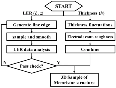
The device geometry variations significantly influence the electrical properties of nano-devicesRoy et al.(2006). For example, the random uncertainties in lithography and pattern-ing processes lead to the random deviation of line edge print-images from their ideal pattern, which is called line edge roughness (LER)Oldiges et al. (2000). Thickness fluctuation (TF) is caused by deposition processes in which mounds of atoms form and coarsen over time. As technology shrinks, the geometry variations do not decrease accordingly. In this work, we propose an algorithm to generate a large volume of three-dimensional memristor structures to mimic the geometry variations for Monte-Carlo simulations. The LER model is based on the latest LER characterization method for electron beam lithography (EBL) technol-ogy from top-down scanning electron microscope (SEM) measurement Jiang et al. (2009). Besides the geometry variations, other process variations such as random discrete doping (RDD) could also result in the fluctuations of the electrical properties of devices. However, because the existing memristors are all based on the thin film deposition technology, the local randomness of RDD is not as significant as geometry variations and is not covered in this work.
1.1.2 Device controllability and stochastic behaviour
At current stage, a large gap exists between the theoretical memristor characteristics and the experimental data obtained from real device development, raising severe concerns in fea-sibility of memristor-based hardware design. For instance, the memristor theory expresses a continuous and stable memristance change. This is the foundation of using memristors to represent synapses in bio-inspired system. Though an arbitrary intermediate state can be obtained by carefully setting current compliance and period in a single metal oxide mem-ristor, e.g., TiO2 device, the corresponding realization at large scale, e.g., cross-point array, is very difficult after including intrinsic design constrains, process variations, environmental fluctuations, etc. Keeping a memristor in its ON or OFF state (corresponding to Ron or
Rof f), on the contrary, is much more controllable. Thus, more precisely, most memristors
Moreover, memristor behaves stochastically and hence even a single memristive device demonstrates large variations in performance. More specific, the static states of a single memristive switch, i.e., Ron and Rof f, are not fixed values, but have large variations with
skewed distributions and heavy tails Yi et al. (2011). The switching mechanism of a mem-ristive switch, that is, its dynamic behavior, performs as a stochastic process Yang et al. (2009). Previous statistical analyses on memristors were limited to the binary switching as storage elements. However, as an analog device in neural network application, it is more important to understand and model memristor’s stochastic characteristics.
1.1.3 Large scale cross-point array analysis
Memristor has demonstrated the similar functions as synapse. Accordingly, memristor cross-point array could be the densest realization of the synapse network among groups of neurons. In human brains, one neuron is usually connected to over thousands of other neurons, which means very large scale cross-point arrays are necessary for direct mapping of synapse network among neurons. However, to simulate the synapse behavior of large scale memristor cross-point array is extremely time-consuming in traditional circuit simulators that were designed for memory applications but not neural network applications. Thus, a circuit simulation platform specially designed for cross-point array as synapse network is an necessary bridge to connect the memristor-based synapse to the memristor-based neuromorphic circuit designs.
1.1.4 Circuit performance analysis base on applications
With enough understanding of memristor devices and memristor cross-point arrays, we can start to explore the realization of ANN algorithms in memristor-based neuromorphic cir-cuits. The study in this area still remains nearly blank at current stage. Though some previous works have analyzed the simple learning behaviors of memristor based synaptic circuits Snider (2008); Jo et al. (2010); Ambrogio et al. (2013); Thomas (2013), the study of the input-output feature of memristor cross-point array is still missing. Moreover, the impact of process variations, signal fluctuations, defects and other physical limitations on memristor-based neuromorphic circuit performance are not yet quantitatively studied.
Furthermore, even though single memristor has been demonstrated with similar functions as synapses, they are still far from even partially mimicking a real biological system. One example is reproducingspatio-temporal property, which is an important synaptic feature denoting the capabilities of not only modulating the strength and rate of an input spike (i.e., spatial weighting) but also adaptively adjusting the synaptic weight according to the relative timing relationship between input and output spikes (i.e., temporal weighting). The requirement of the latter capability is based on the observation that information in biological visual systems is mainly carried by the timing of the first spike and the number of spikes Keat et al. (2001);Gollisch and Meister (2008).
Nowadays, the temporal weighting property usually is realized at software level by inte-grating temporal synapse models into spike-timing-based learning algorithmsMaass(1997); Caporale and Dan (2008); Ponulak and Kasinski (2010). We note that most of synapse designs are based on only multi-level/analog resistance states of memristors by assuming a constant synaptic weight once learning is completed. Such a design without adaptive learn-ing ability may realize either temporal or spatial memory function separately, but cannot offer the combined spatio-temporal property. Moreover, although STDP function has been widely demonstrated on memristors theoretically and experimentally, these designs often require precise neural signals supplied by carefully designed pulse modulatorsSnider(2008); Jo et al. (2010); Ambrogio et al. (2013); Thomas (2013). The incurred design cost is also generally unaffordable for a large-scale neural network implementation.
1.2 CONTRIBUTIONS
To comprehensively address the difficulties mentioned in Section1.1, my study on memristor-based neuromorphic circuits is across device, circuit and application levels. Particularly, the contributions of this thesis can be concluded in the following aspects:
1.2.1 Memristor variation model
For device to device variation, I first investigate the impacts of geometry variations on the electrical properties of memristors and explore their implications to circuit design. An algorithm for fast generation of three-dimensional memristor structures is proposed to mimic the geometry variations incurred by EBL technology. The generated samples are used for Monte-Carlo simulations. Then I develop a fast statistical model to simulate the electrical properties of TiO2 thin-film memristors. Starting with the theoretical model of a TiO2 thin-film memristor, I explore the influences of geometry variations on the electrical parameters of the device. On top of that, a statistical model with the merits of both high accuracy and low runtime cost is proposed. Compared to the previous model, our statistical model significantly improves the runtime cost by 3 ∼ 4 orders of magnitude; and reduces the input data set down to a few variables. The simulation accuracy maintains within∼2% discrepancy in the whole working region of the memristor device.
1.2.2 Memristor stochastic model
For device stochastic behavior, I build a stochastic behavior model of TiO2 memristive de-vices based on the real measurement resultsMedeiros-Ribeiro et al.(2011);Yi et al.(2011) in order to better facilitate the exploration of memristive switches in hardware implementation. The model bypasses material-related parameters while directly linking the device analog be-havior to stochastic functions. Simulations show that the proposed stochastic device model fits well to the existing device measurement results.
1.2.3 Efficient memristor cross-point array simulator
For circuit simulations, I firstly proposed a full dynamic simulation platform of nonlinear memristor crossbar memory, where experimental verified memristor model, nonlinear selector model, stochastic variation model and possible process variations are considered. After taking the regular shape of crossbar array, the simulation process can be speed ed up by 2∼3 orders of magnitudes faster than in SPICE simulation via solving the nonlinear model in
MATLAB environment and pre-calculating its Jacobian matrix. All of these contribute to a simulation study on memristor cross-point array with accuracy and scale which has not been shown before. It can also give us a much deeper insight on the impact of sneak path current leakage, the impact of writing scheme, and the relationship between single memristor device performance and the corresponding crossbar performance.
1.2.4 Memristor-based neuromorphic circuit components
For memristor-based neuromorphic circuit applications, a few memristor-based neuromor-phic circuit components are conducted, including the “macro cell” synapse design, memristor-based stochastic neuron and memristor-memristor-based spatio-temporal (MST)synapse.
“Macro cell” synapse: Macro cell is a practicable neuromorphic circuit design to overcome the gap between the theoretical and real characteristics of memristive devices. A macro cell design is composed of a group of parallel connected memristive switches. It obtains multiple logic states by leveraging device’s stochastic behavior. The macro cell sacrifices the design density for better feasibility. However, it is still more efficient than traditional CMOS implementations through floating gates or capacitors Srinivasan et al. (2005). As a weight storage unit, macro cell synapse can be easily adapted into a cross-point array for high density weight storage. With aid of a feedback attempt scheme, the conductance of a macro cell quickly converges to the desired value.
Memristor-based stochastic neuron: A binary stochastic neuron design can be
realized with a single memristive switch, using an external voltage to control its ON-OFF probability. The design can be extended to continuous stochastic neuron by replacing the memristive switch with the proposed macro cell. The number of switches in macro cell and the external voltage signal together control the mean and deviation of noise.
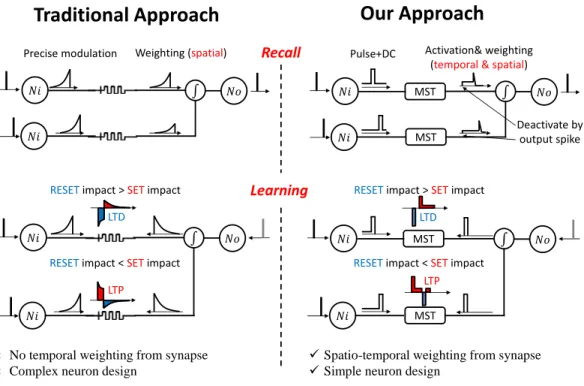
Memristor-based spatio-temporal (MST)synapse: Instead of simplifying synapse
designs, we tend to enrich the functionalities of synapses and reduce the complexity of neurons, as illustrated in Fig.1. The new approach is closer to the fact in biological nervous system and enables a more efficient hardware implementation. In particular, a
Traditional
Approach
Our
Approach
Precise modulation Weighting (spatial)LTD
LTP
Pulse+DC Activation& weighting
(temporal & spatial)
Deactivate by output spike MST MST MST MST LTD
RESET impact <SETimpact
LTP
RESET impact <SETimpact
Learning Recall
× No temporal weighting from synapse
× Complex neuron design
Spatio-temporal weighting from synapse
Simple neuron design
RESET impact >SETimpact RESET impact >SETimpact
Figure 1: Comparison of traditional approach with MST synapse approach.
• A simple and dense structurethat can be easily integrated in cross-point array for massive
connections.
• Relaxed requirements on the control precision of spike signals so that design complexity
of neurons reduces and communication energy efficiency improves.
• Good support of typical synaptic properties, including spike-timing-based recall and synap-tic weight tuning.
• Successful demonstration of spiking-timing-based learning ability by using fundamental
STDP Caporale and Dan (2008) and ReSuMe Ponulak and Kasinski (2010) learning rules.
1.2.5 Memristor-based neurmorphic circuit for spatial pattern recognition
In studying the input-output feature of memristor cross-point arrays, we found this typical array structure can naturally provide the capability of connection matrix storage and matrix-vector multiplication. Moreover, it offers a huge number of connections. Therefore, we exploit the application of the memristor cross-point arrays in neuromorphic hardware design
and use the Brain-State-in-a-Box (BSB) model Hu et al. (2012,2013b), an auto-associative neural network, to illustrate the potential of memristor crossbars in complex and large scale pattern associations and classifications.
Two methods are proposed to configure the memristance of memristor cross-point ar-rays. The mapping method converts a software generated connection matrix into hardware memristor crossbars when memristors can be precisely configured. We present a fast approx-imation technique so that a matrix can be mapped to pure circuit element relations. Key design parameters and physical constraints have been extracted and carried into the study of the accuracy and robustness of the BSB circuit. Interestingly, the large random process variations of the memristive devices Hu et al. (2011b); Medeiros-Ribeiro et al. (2011) have little adverse impact, due to the inherent random noise tolerance of the BSB model.
The training method mimics the training process in the software algorithm and iterative-ly adjusts the memristor cross-point arrays to the required status. Many physical constraints in circuit implementations have been considered, including limited data access, limited accu-racy of signal detection, non-ideal memristor characteristics Strukov et al. (2008b), process variations and defects. Our design generates the programming pattern for iterative training using the sign of input signals and the magnitude differences between the output signals and the expected outputs. By avoiding directly reading the memristance values of cross-point arrays, the proposed scheme significantly reduces the design complexity and avoids analog-to-digital converter (ADC) circuits. We demonstrate the effectiveness of our training scheme by performing the recall operation with the BSB recall circuit and comparing the results with those from software algorithms Lillo et al. (1994); Perfetti(1995); Park (2010).
1.2.6 Memristor-based spiking neurmorphic circuit for temporal pattern recog-nition
With the MST synapse which can mimic the spatio-temporal feature of synapse, we are able to build efficient memristor-based neuromorphic circuit to realize the spiking neural network for temporal learning algorithms. we studied the usage of MST synapses in spiking neural networks for a temporal pattern learning task with both STDP and ReSuMe learning rules.
Our result shows that the learning task can be accomplished at nano-second scale with on average 36.7pJ and 64.0pJ per learning spike for STDP and ReSuMe learning rules, respec-tively. And the recall energy consumption is only 14.6pJ per recall spike. Even with All the simulations are conducted with the latest experimentally-grounded TaOxphysical model from HP Labs Strachan et al. (2013), making great promise of the credibility of the work. Even the MST synapse design based on TaOxdevices has limited synaptic conductance tun-ing range, our result shows that it can still provide sufficient learntun-ing ability in neural network applications with assist of appropriate learning rules. Further increase of memristance range will alleviate the situation and makes more learning rules practical. Note that the micro model of TaOx devices used in this work has a low resistance range of 70Ω∼670ΩStrachan et al. (2013). Applying nano-scale devices can significantly increase the memristance value to 100KΩ∼1MΩJo et al. (2010) and further reduce energy per spike to the sub-pJ region.
1.3 THESIS ROADMAP
The rest of the paper is organized as follows: Chapter 2 introduces preliminary knowl-edge on memristor, synapse and neural networks Chapter 3 describes the modeling work of memristors on device variation and stochastic behavior. Chapter 4 briefly explains the MATLAB-based memristor cross-point array simulator and verifies the result. Chapter 5 introduces the memristor-based neuromorphic circuit components. Chapter 6 details the implementation of BSB neural network with memristor-based neuromorphic circuit for spa-tial pattern recognition. Chapter 7 describes the implementation of spiking neural network with memristor-based neuromorphic circuit for temporal pattern recognition. Chapter 8 concludes the thesis.
2.0 PRELIMINARY
2.1 MEMRISTOR
2.1.1 Theoretical memristors
The original definition of the memristor is derived from circuit theory: besides resistor, capacitor and inductor, there must exist the fourth basic two-terminal element that uniquely defines the relationship between the magnetic flux (ϕ) and the electric charge (q) passing through the device Chua (1971a), or
dϕ=M ·dq. (2.1)
Considering that magnetic flux and electric charge are the integrals of voltage (V) and current (I) over time, respectively, the definition of the memristor can be generalized as:
V =M(ω, I)·I dω dt =f(ω, I) (2.2)
Here, ω is a state variable; M(ω, I) represents the instantaneous memristance, which varies over time. For a “pure” memristor, neither M(ω, I) nor f(ω, I) is an explicit function of I Strukov et al. (2009).
Doping front Voltage L z h R R (a) Pt Pt TiO2 TiO2-x RL·α RH·(1-α) (a) (b)
Figure 2: TiO2 thin-film memristor. (a) structure, and (b) equivalent circuit.
2.1.2 Memristor devices
2.1.2.1 TiO2 thin-film memristor In 2008, HP Lab demonstrated the first intentional memristive device by using a Pt/TiO2/Pt thin-film structure Strukov et al. (2008a). The conceptual view is illustrated in Fig. 2(a): two metal wires on Pt are used as the top and bottom electrodes, and a thick titanium dioxide film is sandwiched in between. The sto-ichiometric TiO2 with an exact 2:1 ratio of oxygen to titanium has a natural state as an insulator. However, if the titanium dioxide is lacking a small amount of oxygen, its con-ductivity becomes relatively high like a semiconductor. We call it oxygen-deficient titanium dioxide (TiO2−x) Niu et al.(2010). The memristive function can be achieved by moving the
doping front: A positive voltage applied on the top electrode can drive the oxygen vacancies into the pure TiO2 part and therefore lower the resistance continuously. On the other hand, a negative voltage applied on the top electrode can push the dopants back to the TiO2−x
part and hence increase the overall resistance. For a TiO2-based memristor,RL(RH) is used
to denote the low (high) resistance when it is fully doped (undoped).
Fig. 2(b) illustrates a coupled variable resistor model for a TiO2-based memristor, which is equivalent to two series-connected resistors. The overall resistance can be expressed as
M(w) = RL·ω+RH ·(1−ω). (2.3)
Here ω (0≤ ω ≤ 1) is the relative doping front position, which is the ratio of doping front position over the total thickness of TiO2 thin-film.
The velocity of doping front movementv(t), which is driven by the voltage applied across the memristor V(t) can be expressed as
v(t) = dω dt =µv· RL h2 · V(t) M(ω) (2.4)
where,µv is the equivalent mobility of dopants,his the total thickness of the TiO2 thin-film; and M(ω) is the total memristance when the relative doping front position is ω.
Bulk model is a general model derived from the mathematical definition of memristor, which assumes a flat doping front moving up or down. However, in reality, filamentary conduction has been observed in nano-scale semiconductors: the current travels through some high conducting filaments rather than passes the device evenly Kim et al. (2006)Kim et al. (2007). The doping front is formed so randomly that a few filaments dopes much faster than others, observed as hot spots on the device. This is called asfilament conduction
phenomenon. The way we solved the conflict between the bulk and filament models in this
work can be explained as follows: when cutting the device into many tiny tiny filaments as we shall describe in Section3.1.1, it is reasonable to assume a small flat doping front exists in each filament. Therefore, bulk model can be used for each small flat doping front movement. Recent experiments showed that µv is not a constant but grows exponentially when the
bias voltage goes beyond certain threshold voltage Strukov and Williams (2009). Neverthe-less, the structure of TiO2 memristor model, i.e., Eq. (2.4), still remains valid.
2.1.2.2 Spintronic memristor The spintronic memristor relies on the existence of do-main wall in MTJ free layerLou et al.(2008) and properly controlling the domain wall. There have been many research activities on manipulating domain walls Parkin (2009)Tatara and Kohno (2004)O. Boulle and Klaui (2011). Very recently, NEC Lab reported the free layer switching though the domain wall movement Matsunaga et al. (2011), which indeed is a spintronic memristor.
Among all the spintronic memristive devices , the one based on magnetic tunneling junction (MTJ) could be the most promising one because of its simple structureWang et al. (2009)Wang and Chen (2010). The basic structure of magnetic memristor could be either giant magneto-resistance (GMR) or tunneling magneto-resistance (TMR) MTJs. We choose
Metal Free layer Metal Reference layer Voltage Domain wall (a) (b) R H /(1 -α ) R L/ α L z h
Figure 3: TMR-based spintronic memristor. (a) structure, and (b) equivalent circuit.
TMR-based structure shown in Fig.3(a) as the objective of this work because it has a bigger difference between the upper and the lower bounds of total memristance (resistance).
An MTJ is composed of two ferromagnetic layers and an oxide barrier layer, e.g. MgO. The bottom ferromagnetic layer is called reference layer, of which the magnetization direction is fixed by coupling to a pinned magnetic layer. The top ferromagnetic layer called free layer is divided into two magnetic domains by a domain-wall: the magnetization direction of one domain is parallel to the reference layer’s, while the magnetization direction of the other domain is anti-parallel to the reference layer’s.
The movement of the domain wall is driven by the spin-polarized current, which passes through the two ferromagnetic layers. For example, applying a positive voltage on free layer can impel the domain wall to increase the length of the magnetic domain with a magnetization direction parallel to the reference layer’s and hence reduce the MTJ resistance. On the other hand, applying a positive voltage on reference layer will reduce the length of the magnetic domain with a magnetization direction parallel to the reference layer’s. Therefore, the MTJ resistance increases. If the width of the domain with the magnetization direction anti-parallel (parallel) to the reference layer’s is compressed to close to zero, the memristor has the lowest (highest) resistance, denoted as RL (RH).
As shown in Fig. 3, the overall resistance of a TMR-base spintronic memristor can be modeled as two parallel connected resistors with resistances RL/ω and RH/(1−ω),
respec-tivelyWang and Chen (2010). This structure has also been experimentally provedLou et al. (2008). Here ω (0≤ω ≤1) represents the relative domain wall position as the ratio of the
domain wall position (x) over the total length of the free layer (L). The overall memristance can be expressed as
M(α) = RL·RH
RH ·ω+RL(1−ω)
. (2.5)
How fast the domain-wall can move is mainly determined by the strength of spin-polarized current. More precisely, the domain-wall velocity v(t) is proportional to the current density
J Li and Zhang (2004). We have
J(t) = V(t) M(ω)·L·z, (2.6) and v(t) = dω(t) dt = Γv L ·Jef f(t),Jef f = J,J ≥Jcr 0,J≤Jcr. (2.7)
Here Γv is the domain wall velocity coefficient, which is related to device structure and
material property. L and z are the total length and width of the spintronic memristor, respectively. The domain wall movement in the spintronic memristor happens only when the applied current density (J) is above the critical current density (Jcr)Li and Zhang(2004);
Bazaliy and et al (1998);Zhang and Li (2004); Liu et al. (2005); Tatara and Kohno(2004).
2.1.3 Characteristics of realistic memristive devices
Compared to theoretical characteristics of ideal devices, many non-ideal features have been revealed in real memristive devices. Large device to device variation is one of the issue since memristor is still in its infancy and its compact nano-size structure also aggravate the problem. Since memristor is using the same fabrication process as traditional CMOS technology, the CMOS process variation analysis method will be adopted in our following analysis scheme.
More importantly, although a single memristor can be carefully tuned to arbitrary analog states, this approach cannot be generalized to a large-scale implementation, e.g., a cross-point array with a large number of memristors. We have to face the unfortunate reality that only memristive switches presenting binary states are available in memristive system design Ha and Ramanathan (2011).
Moreover, the stochastic behavior in dynamic switching process and large variations in static states have been widely observed in experimental results of metal oxide materials, such as TiO2 based memristive switches. In brief, the time to successfully change the state of a single memristive switch is not deterministic but follows a wide lognormal distribution Medeiros-Ribeiro et al. (2011). And its resistance in ON or OFF state (Ron orRof f,
respec-tively) is not a fixed value, but follows a skewed, heavy tail distribution Yi et al. (2011). These non-ideal characteristics shall be considered in hardware implementations built with memristive switches.
There are many physical memristor models based on insight mechanisms Yang et al. (2009); Miao et al. (2009); Pickett et al. (2009). These models are deterministic so cannot reflect the large variation induced by stochastic switching behavior. Stochastic models can better link the statistical measurement data to probability functions. However, the existing stochastic models are limited to only the binary switching behaviors Medeiros-Ribeiro et al. (2011); Yi et al. (2011). Without considering the stochastic switching of memristor, the intermediate analog state cannot be captured.
2.2 SYNAPSE THEORY
Originallysynapse is used in biological systems, representing the communication channel of electrical/chemical signals. Later on, the use of synapse was expended to computer science and neuromorphic hardware in developing brain-like computing systems. The use of synapse was then expended to neuromorphic hardware in developing brain-like computing systems. Though the meanings of synapse in these areas share high similarity, there are many subtle differences.
2.2.1 Biological Synapse
The weighting function of biological synapse has been widely taken as a spatio-temporal
activated by the input spikes from pre-neurons Gollisch and Meister (2008). For instance, the low response variability of retinal ganglion cells shows that the most important info of a firing event by visual neurons is reserved by the timing of the first spike and the number of spikes Keat et al. (2001). Experiments also show that the timing of the first spike after stimulus onset carries the majority of the visual info Gollisch and Meister (2008).
The tuning of synaptic strength has two important properties: long term potentiation
(LTP) represents a long lasting strength potentiation once a synapse receives strong and positive stimulus from active connections, and long term depression (LTD) is an opposite process. The effects of LTP and LTD are strongly related to the spiking time, initial synaptic strength, and type of post-synaptic cells Bi and Poo (1998). More importantly, biological synapses have self-learning abilities, e.g., spike-timing-dependent plasticity (STDP) Bi and Poo (1998). Experiment of cultured hippocampal neurons showed that within a critical correlation time window, the post-synaptic spiking that peaked after synaptic activation caused LTP, whereas the post-synaptic spiking before synaptic activation resulted in LTD Bi and Poo (1998).
2.2.2 Artificial Neural Network (ANN) Synapse
ANNs are computational models that mimic nervous systems for machine learning and pat-tern recognition. ANN synapses are expressed by highly abstracted models of the biological version. Usually here synaptic strength is converted to synaptic weight, since it could be negative in ANN meanings.
There are different ways to employ ANNs in recall process. For instance, feedforward neural network can be considered as spatial mapping, in which synapses maintain constant weights and provide consistent weighting functions, while a neuron output is determined by its net-input at each time step. In contrast, spiking neural networks can provide temporal mapping: a neuron accumulates the net-input and fire a spike once the accumulation reaches the threshold. One of these procedures is refined as theleaky-integrate-and-fire (LIF) model [16]. Synaptic weights are either keep consistent, result inrate-codedrecall where information is carried by rate of spikes, or updated dynamically depending on the timing of spikes,
lead to temporal-coded recall that information is carried by precise timing of spikes For the latter part, STDP learning rule is a well-known example, which is abstracted from the biology observation; The hierarchical temporal memory (HTM) model HTM (2011)also employee the temporal feature of synapse in a highly abstracted manner: each synapse has a permanence value that consistently decreases over time, and the permanence value increases only when the synapse receives an input spike that activate it. Synaptic weight changes to 1 if permanence value is beyond threshold, otherwise it is 0. However, spatial and temporal weighting properties of synapse in ANNs are separated since it is usually considered as a single number.
The synaptic weight modification can integrate into the learning process. Among a vari-ety of learning algorithms in ANN family,Hebbian rule and Delta rule are two fundamental methods. In Hebbian rule, the synaptic weight between two neurons increase (decreases) when they activate simultaneously (separately). Delta rule improves Hebbian rule’s learning quality by consider output signal as feedback to minimize the spatial error between target signal and output signal. Note that basic Hebbian and Delta rules are spatial learning algo-rithms because their weight modifications are determined solely by the signals at the current time step. For spiking neural networks, STDP rule can be regarded as an improved version of Hebbian rule in temporal space as it considers the time correlation between pre-spike and post-spike to modify the synaptic weight. Similar as Delta rule, ReSuMe improves STDP rule’s performance by minimizing the temporal difference between target spikes and output spikes. Both STDP and ReSuMe are temporal learning algorithms and they will be detailed in Section II.B.
2.2.3 Electronic Synapse
ANN algorithms have obtained great achievement in many applications. However, the per-formance of such pure software-level applications is severely limited by the traditional von Neumann architecture, as the “memory wall” problem we mentioned before.
The use of synapse has been expended to neuromorphic hardware in developing brain-like computing systems. Neuromorphic circuits tend to mimic biological models and employ
I N P U T O U T P U T Synapse network a group of mneurons
with activity pattern F
a group of nneurons
with activity pattern T
Figure 4: A simple example of neural network.
the same operation flows in weighting, tuning, and learning processes. Previously, SRAM, floating gates, capacitors have been used in developing electronic synapses Mead and Ismail (1989). As aforementioned, these designs are severely constrained by parallelism scale and implementation size Merolla et al. (2011); Seo et al. (2011). Another prominent trend is designing electronic synapses and neurons in analog or mixed-signal format. The process variations and signal fluctuation can dramatically affect the system performance, which however can be partially amortized by synapse’s learning ability.
The recently re-discovered memristor devices at nanometer scaleJo et al.(2010) demon-strate synapse-alike behaviors, offering a more efficient way to implement electronic synapses. For instance, Snideret al. successfully realized LTP, LTD, and STDP in a TiO2 device con-trolled by pulse width modulators (PWM) Snider (2008). The similar functions were also obtained in Ag/Si memristor synapse by using time division multiplexing (TDM) Ambrogio et al.(2013). Very recently, a 1T1R-based HfO2 synapse was demonstrated with pulse shape filters in pre- and post-neurons Thomas(2013). These demonstrations remain at single de-vice level and require complicated neuron circuits. To the best knowledge of authors, the spatio-temporal feature has never been presented in electronic synapse designs.
2.3 NEURAL NETWORK
Figure 4 illustrates a simple example of a neural network, in which two groups of neurons are connected by a set of synapses. We define ai,j as the synaptic strength of the synapse
connecting the jth neuron in the input group and the ith neuron in the output one. The
relationship of the activity patterns F of input neurons and T of output neurons can be described in matrix form:
Tn=An×m×Fm, (2.8)
where matrix A, denoted as the connection matrix, consists of the synaptic strengthes be-tween the two neuron groups. The matrix-vector multiplication of Eq. (2.8) is a frequent operation in neural network theory to model the functionally associated with neurons in brains.
2.3.1 Brain-state-in-a-Box neural network for spatial learning
The BSB model is an auto-associative neural network with two main operations: training and recall Anderson et al. (1977). The mathematical model of BSB recall function can be represented as Wu et al. (2011):
x(t+ 1) =S(α·Ax(t) +β× ·x(t)), (2.9) where,xis anNdimensional real vector, and Ais anN-by-Nconnection matrix. Ax(t) is a matrix-vector multiplication, which is the main function of the recall operation. α is a scalar constant feedback factor. β is an inhibition decay constant. S(y) is the “squash” function defined as follows: S(y) = 1, if y≥1 y, if −1< y <1 −1, if y≤ −1 . (2.10)
For a given input pattern x(0), the recall function computes Eq. (2.9) iteratively until con-vergence, that is, when all the entries of x(t+ 1) are either ‘1’ or ‘−1’.
The most fundamental BSB training algorithm is given in Figure 5, which bases on the extended Delta ruleAnderson et al.(1977). It aims at finding the weights so as to minimize
Figure 5: BSB training algorithm using Delta rule.
the square of the error between a target output pattern and the input prototype pattern. A large α helps improve the training speed but may cause non-convergence. On the other hand, if α is too small, the convergence needs many iterations. The best α usually can be obtained through experimentation. In neuromorphic hardware, the training terminates once its error drops below a predefined threshold, represented by a reference voltage in this work.
A typical application of the BSB model isoptical character recognition(OCR) for printed textSchultz (1993). A multi-answer character recognition method based on the BSB model has been developed to improve reliability and robustness for noisy or occluded text images Wu et al. (2011). The method first performs a training (pattern memorization) operation on all BSB models such that they “remember” different character patterns. Once trained, input character images can be processed through multiple BSB modules in parallel for the recall (pattern recognition) operation. When all recalls are complete, a set of candidates is selected based on the convergence speed and provided for cogent confabulation-based word or sentence completion Qiu et al. (2013, 2011). This method will be used to evaluate the reliability and robustness of the proposed memristor-based BSB recall circuit.
Latency encoding 0 1 2 3 4 5 6 7 8 9 10 Time steps # ne ur on s 0 1 2 3 4 5 6 7 8 9 10 Time steps # ne ur on s Ali gn me n t Compr es sion Pattern
Spike timing train T photoreceptor cells RGCs Image signal Spike trains Neuron network Target pattern “beauty” Receiving Encoding Learning
(a) (b) (c)
Figure 6: A spike-timing-based model for spatio-temporal pattern recognition. (a) The overview of the spike-timing-based model for vision system; (b) A general LPE flow; (c) An example of spatio-temporal pattern conversion: the image “5” is partitioned and converted to multiple spike-timing trains.
2.3.2 Spiking neural network for temporal learning
Spiking neural networks with temporal codes mimic human vision system for spatio-temporal pattern recognition, demonstrating very high efficiency. Fig. 6(a) illustrates that in human retina, visual signals from 108 photoreceptor cells are projected to 106 retinal ganglion cells (RGCs) in a form of spike trains (temporal codes) through temporal encoding Meister and Berry II (1999). These spikes are then processed and learned through spike-timing-based
recall and spike-timing-based learning processes Hu et al. (2013a). We will take such a
temporal pattern learning task in Section7.2 as a case study to examine the performance of MST synapses. The application requires the following three main functions:
Temporal Encoding: We use latency-phase encoding (LPE) in Fig. 6(b) to explain how to convert a spatial pattern (e.g., sensory stimuli) into a single spike-timing train Hu et al. (2013a). For a pattern vector, the different locations of variables are encoded into the different phase delays of sinusoid waves. And the amplitude of a variable is represented by the relative timing within the time window of a spike-timing train. Limited by the capacity of spike-timing train, large patterns usually are partitioned and converted into multiple spike-timing trains, as shown in Fig.6(c). This is so-called spatio-temporal pattern.
− + − +− −+ +/− (a) (b) + − − +
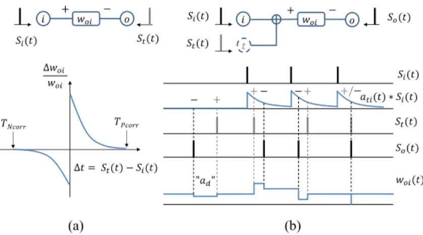
Figure 7: Spike-timing-based learning rules and diagrams of neuron connections. (a) STDP learning rule; (b) ReSuMe learning rule.
Spike-timing-based Recall: Unlike spike-rate-based recall, in which the information communication is mainly determined by the rate of input spikes, spike-timing-based recall
concerns more on their relative timing. In spike-timing-based recall, the relative timing between input and output spikes changes the temporal weight of a synapse (e.g., activated or deactivated) and enables the neural network to produce the desired temporal patterns. The spatial weights of synapses remain unchanged during the entire recall process.
Theoretically, two design approaches can be used to realize the spike-timing function. One attempt is to convert input spike signals into decayed traces to represent the temporal impact. For example, many neuromorphic circuits incorporate an input spike train Si(t)
with a shape modulation term ati(t) at the input neuron. Si(t) is then transferred into
the convolution form ati(t)∗Si(t) and passed to the synapse, as illustrated in Fig. 7(b).
The synapse performs only spatial weighting function and its weight remains constant in recall. However, complex neuron designs, such as PWM and TDM components, usually are required to provide precise timing controls Snider (2008); Ambrogio et al. (2013). Another approach is adopting temporal synapse which changes synaptic weights over time Ponulak and Kasinski (2010). It can greatly simplify the neuron design. However, synapse’s spatial weight is unclear and the synapse design itself becomes very complex.
Spike-timing-based Learning: Most of the spike-timing-based (temporal) learning algorithms can be generalized from the fundamental STDP and ReSuMe learning rules. Let’s take a simple structure of one synapse connecting two neurons as an example.
In STDP learning process, the post-neuron is forced to fire the target spike train St(t).
If an input spike at the pre-neuronSi(t) occurs within a predefined positive correlation time
window (TP corr) before St(t), such as 0 ≤ ∆t = St(t)−Si(t) < TP corr, implying the two
neurons have a positive correlation, the synaptic weight in between increases. In contrast, a connection of two negative correlated neurons within a negative correlation time window
(TN corr) shall be weakened. Fig. 7(a) shows a typical dependence of the synaptic weight
change rate on ∆t.
The learning efficiency of STDP severely relies on the correlation of the input and target spikes. When a target spike is uncorrelated to any of the input spikes, the STDP learning process fails. Thus, more input neurons firing at various patterns are needed to increase the learning capacity of neural networks.
Unlike STDP, the ReSuMe learning rule requires output spikes to participate in the learning process and introduces a cost function to minimize the error between the target and the output spikes. As illustrated in Fig. 7(b), input spikes are first converted to decayed traces and then combined with the target spikes. The produced output spike will be fed back to synapses to assist weight updating. As such, the change of synaptic weightwoi from
pre-neuron i to post-neurono can be described as follows:
d
dtwoi(t) = [St(t)−So(t)][at+
Z ∞
0
ati(s)Si(t−s)ds], (2.11)
whereatis a constant that helps speed up the learning process, and ati(t) is a shape
modula-tion term which convertsSi(t) to decayed traces. Eq. (2.11) implies that the synaptic weight
woi is updated when St(t) 6= So(t). The direction and magnitude of the weight tuning are
3.0 MEMRISTOR MODELS FOR CIRCUIT SIMULATION
3.1 MEMRISTOR VARIATION MODEL
3.1.1 Mathematical analysis
The actual length (L) and width (z) of a memristor is affected by LER. The variation of thickness (h) of a thin film structure is usually described by TF. As a matter of convenience, we define that, the impact of process variations on any given variable can be expressed as a factor θ = ω
0
ω, whereω is its ideal value, and ω
0 is the actual value under process variations.
The ideal geometry dimensions of the TiO2 thin-film memristor and spintronic memristor used in this work are summarized in TABLE 1.
3.1.1.1 TiO2 thin-film memristor In TiO2 thin-film memristors, the current passes through the device along the thickness (h) direction. Ideally the doping front has an area
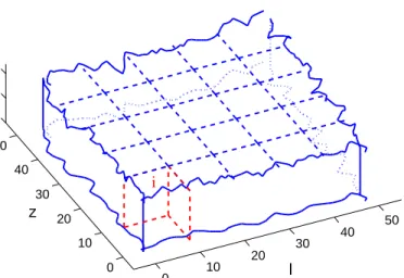
S =L·z. To simulate the impact of LER on the electrical properties, the memristor device is divided into many small filaments between the two electrodes. Each filament i has a cross-section area ds and a thickness h. Fig. 8 demonstrates a non-ideal 3D structure of a TiO2 memristor (i.e., with geometry variations in consideration), which is partitioned into many filaments in statistical analysis.
Table 1: The Device Dimensions of Memristors.
Length(L) Width(z) Thickness(h) Thin-film 50 nm 50 nm 10 nm Spintronic 200 nm 10 nm 7 nm