www.ijraset.com Volume 5 Issue VI, June 2017 IC Value: 45.98 ISSN: 2321-9653
International Journal for Research in Applied Science & Engineering
Technology (IJRASET)
©IJRASET: All Rights are Reserved
2478
Comparative Study Between Different Metal Gates
Engineered Structures
L. M. Gupta1, Neeraj Gupta2
Assistant Professor, ECE Department, ASET, Amity University, Haryana
Abstract: In this paper, comparative study between different metal gate structures has been presented. Short channel effect acts as barrier for further reduction in size of conventional MOSFETs. So looking for new device structures with different materials and property. But this alone cannot help us to catch up the ITRS roadmap. To achieve this, proportional decrease in oxide thickness are required. But SCEs are come into the picture again and degrade the device performance. So introduced the concept of dual dielectric along with different metal gate and this concept enhance the performance of device. The comparisons between devices are carried out by using surface potential and electric field parameters. The triple metal dual dielectric cylindrical gate all around MOSFETs are the best device among all. The comparisons are carried out with the help of MATLAB. Keywords: MOSFET, Metal Gates, Dielectrics, potential, field, Work function
I. INTRODUCTION
MOSFET has become the most essential and fundamental building block of VLSI circuits due to its inimitable properties. The aggressive downscaling of conventional MOSFETs is required to fulfill the demand for higher packing density, high speed, low power consumption and low cost.
Obviously, the motive of miniaturization is to deliver high performance at lower cost. Smaller circuit dimensions reduce the overall chip area, thereby allowing more transistors to be fabricated on single ICs. On decreasing the MOSFET dimensions, the switching delay of devices decreases linearly.
This is mainly due to the delay time is approximately equal to channel length/carrier velocity.
The tremendous advantage of miniaturization is the reduction of power consumption which is not only useful for mobiles to lengthen battery life, but also for improving the reliability of high performance systems. But conventional MOSFET suffers from effect known as “short-channel effect” (SCE) of MOSFETs and is often measured as the threshold voltage reduction of MOSFETs with short-channel length. To improve the immunity against the short channel effects, the dual metal gate, triple metal gate has been used. As the name suggests, the gate terminal consists of three/ two metals in this structure with different work functions. Such a structure provides simultaneous increase in
transconductance to drain current ratio and suppressed SCEs due to a step change in the surface-potential profile in comparison with a single gate MOSFETs. In order to include the advantages of both gate material and gate stack structures, a new device structure is introduced which is known as metal gate dual dielectric (MGDD) structures.
Section 2 describes the design approaches for MOSFETs. In section 3 the comparative study between the single metal, double metal and triple metal gates are presented using MATLAB. The section 4 closed with conclusion and future work.
II. DESIGN APPROACHES
There are various design approaches. Some authors used multi gate approaches and some used dual dielectric approaches. But this paper presents mixture of two approaches. This mixed approach is used to carry out the comparative study.
increases sharply at the interface of the two gate material which further results in the increased gate transport efficiency [2-3]. The Cylindrical Gate all around (CGAA) MOSFET is considered as one of the most promising devices for downscaling below 100 nm. The CGAA MOSFETs can achieve a higher packing density due to their enhanced current drive compared to planar MOSFETs. However, even in CGAA MOSFET devices, SCEs such as the threshold roll-off, DIBL and the subthreshold swing degradation cannot be neglected from channel lengths below 100 nm. But by incorporating the triple metal/dual metal gate structure along with dual dielectric improve the performance. In the Metal gate structure, The field at the drain end is decreased, which ensures that the field under the gate is increased. This step change in the function profile of the surface potential ensures screening of the channel region under the material on the source side from drain-source potential variations. After saturation higher metal gate work function region absorbs any additional drain-source voltage and hence, the region under lower metal gate work function region is screened from drain –source variations[6-7].
Miniaturization of the devices also requires the gate oxide thickness to be reduced in proportion to channel length. This is essential in order to keep better gate control over the channel as compared to drain. However, continuous scaling of gate dielectric thickness results in enhancement in gate leakage current and which causes increase in static power consumption. In order to resolve the above issues, alternative gate dielectrics are considered. Traditional SiO2 is being replaced by high-K dielectrics to reduce the gate leakage current. Silicon with high-K material systems might suffer from interface trap states and low mobility.
High-K gate dielectric along with SiO2 is a possible solution to replace thinner silicon-dioxide layer in a nanoscale MOSFETs [3], [8].
III. SIMULATION AND RESULTS
All the simulations are done using MATLAB tool. The present simulation is carried out for surface potential and electric field for SMDDCGAA, DMDDCGAA and TMDDCGAAA MOSFETs. Simulation parameters are: Vgs=0.2V, Vds=0.05V, toxeff=2 nm ,
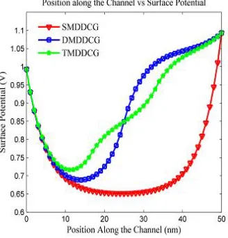
Nak=1020 cm-3, Nd=1020 cm-3, L=50nm. The surface potential of multi gate MOSFETs structure is shown in figure 1.
Figure 1 depicts that triple metal dual dielectric structure has two step function profile which clearly indicates reduction in SCEs. These steps function profile at the interface of two metal regions suppress the higher metal gate work function region from the
variation of drain bias. Increased drain biasis dropped across the lower metal gate work function region. It is also noticed that triple
[image:3.612.223.387.448.619.2]metal dual dielectric MOSFETs have minimum surface potential, an extra step profile as compared to the single metal and dual metal dual dielectric CGAA MOSFETs. So TMDDCGAA have better performance and enhanced immunity against SCEs [4-5].
Figure 1: Position along the channel length and surface potential for SMDDCGAA, DMDDCGAA and TMDDCGAA MOSFETs
www.ijraset.com Volume 5 Issue VI, June 2017 IC Value: 45.98 ISSN: 2321-9653
International Journal for Research in Applied Science & Engineering
Technology (IJRASET)
©IJRASET: All Rights are Reserved
2480
Figure 2: Position along the channel length and electric field for SMDDCGAA, DMDDCGAA and TMDDCGAA MOSFETs
IV. CONCLUSION AND FUTURE WORK
This paper concludes that triple metal dual dielectric cylindrical gate all around MOSFETs shows superior performance as compared to SMDDCGAA and DMDDCGAA MOSFETs. The surface potential and electric field exhibits extra step function profile in TMDDCGAA MOSFETs which significantly reduce the SCEs. In future, the performance can be further enhanced by using halo concept.
REFERENCES
[1] W. Long, H K Jm and Chin, “Dual material gate field effect transistor”, IEEE Transactions on Electron Devices. Vol.46, no.5, pp. 865-870, 1999.
[2] C.J. Pravin, D. Nirmal , P. Prajoon and J. Ajayan,” Implementation of nanoscale circuits using dual metal gate engineered nanowire MOSFET with high-k dielectrics for low power applications”, Physica E: Low Dimensional Systems and Nanostructures vol. 83, pp. 95–100, 2016.
[3] P. Ghosh , S. Haldar ,R.S. Gupta and M. Gupta,”Analytical modeling and simulation for dual metal gate stack architecture cylindrical/surrounded gate MOSFET”, Journal of Semiconductor Technology and Science, vol. 12 issue 4, pp. 458-463, 2012
[4] MATLAB Manual 2013.
[5] S. Dubey,A. Santra,G. Saramekala , M. Kumar and P.K. Tiwari,” An analytical threshold voltage model for triple-material cylindrical gate-all-around (TM-CGAA) MOSFETs”, IEEE Transactions on Nanotechnology, vol. 12 issue 5 , pp. 766-774, 2013.
[6] Neeraj Gupta, Janak Kumar B. Patel, A.K.Raghav, "A Study of Conventional and Junctionless MOSFET Using TCAD Simulations", International conference on advanced computing and communication technologies, IEEE 2015, DOI: 10.1109/ACCT.2015.51.
[7] Neeraj Gupta, Janak Kumar B. Patel, A.K.Raghav, "A study on roadmap for future multi gate SOI mosfet",international journal of engineering research vol. 3, no.1, p.p. 1-7, January 2015.