FPGA-BASED HARDWARE DESIGN OF CLOSED LOOP
CONTROL FOR FIBER OPTIC GYROSCOPE
1Q. D. SUN, 2Z. H. ZHU, 3B. P. LAROUCHE
1Assoc. Prof., School of Electronic and Electrical Engineering, Shanghai Second Polytechnic University,
2360 Jinhai Road, Shanghai, 201209, China
2Assoc. Prof., Department of Earth and Space Science and Engineering, York University, 4700 Keele
Street, Toronto, ON, M3J 1P3, Canada
3Dr, Department of Earth and Space Science and Engineering, York University, 4700 Keele Street,
Toronto, ON, M3J 1P3, Canada
E-mail: [email protected], [email protected], [email protected]
ABSTRACT
The stability, reliability and miniaturization of fiber optic gyroscope (FOG) are always the research focuses and difficulties. This paper presented a hardware design method for the digital closed loop control system of FOG based on FPGA. Based on a large number of experiments, this paper summarized the parameter demands for each module of closed loop control circuit and designed a corresponding hardware circuit using FPGA. The proposed twice closed loop technique improved the zero offset stability of FOG. The using of FPGA brought the digital signal processing by software, the system reliability and agility enhancement as well as the system miniaturization. Particularly, we discussed the problems of component selection and the anti-jamming measures for PCB design to improve the performances of the system. We also developed some samples of FOG using this design method. The experiments and tests show that the proposed method is efficient and valuable. The zero-biases of all samples are all less than 0.075deg/h.
Keywords: Fiber Optic Gyroscope, Hardware Design, Digital Closed Loop, Second Closed Loop, FPGA
1. INTRODUCTION
As a novel angular rate sensor, the fiber optic gyroscope (FOG) has many advantages, such as completed solid state, small size, light weight, long using life, low cost and high anti-impact capability [1]. It has been paid widely attention by the world and increased investment in its research and development annually. It also has been applied to the field of the inertial measurement in the areas of space productions, military productions and civilian productions.
The basic principle of interferential FOG based on the Sagnac effect [2]-[7] and the reciprocity theorem of its component are introduced in this paper. The work characteristics of the digital closed loop applied to FOG are also analyzed. According to the design requirements, the digital closed loop feedback control system of FOG is implemented. On the basis of the amount of testing, the parameter adjustments of modules in the closed loop control system are summarized, and the relevant circuit is schemed out. At the same time, we discuss the component selection and the issues of anti-jamming in PCB design in detail. Finally, we develop some
samples of FOG using the hardware design method proposed in this paper and combining the relevant software development in FPGA.
This paper is organized as follows. In section 2, we introduce the control technique of digital closed loop for FOG. Section 3 presents the circuit design method of digital closed loop system for FOG in detail. Section 4 gives some considerations for the hardware design and shows a good performance of FOG samples through experiment testing. Section 5 gives the conclusions of this paper.
2. TECHNIQUE OF DIGITAL CLOSED LOOP FOR FOG CONTROL
A. Main Frame
The typical system mainly consists of optical source generator, photoelectric detector, A/D convertor, digital logic module, D/A convertor,
optical integrated component (coupler,
[image:2.612.314.524.277.457.2]Y-waveguide) and optical fiber ring [8]-[10]. Its frame is shown as in Fig. 1. In this system, we input the phase modulation signals with the ladder wave and square wave into the interferometer through the optical integrated component. The ladder wave is applied to counteract the Sagnac phase shift through closed loop feedback control. The square wave is as an offset signal to enable that the output signal of the Sagnac interferometer has a linear relationship with the phase shift signal. The step height of the ladder wave is the measured Sagnac phase shift, which is the angular rate signal. In this scheme, besides the output of detector, the drive signals of ladder wave and square wave, the main signal processing is done in the digital field to avoid the circuit noises and to improve the measuring precision [11]. Hence, this scheme is one of the main methods of signal processing system for the medium or high precision FOG.
Figure 1. The Frame Of Closed Loop Control System Of FOG.
B. Basic Principle
The phase difference of FOG can be obtained through measuring the intensity of the output of the
photoelectric detector. The light intensity variable P
of the output from the Sagnac interferometer has a
relationship with the Sagnac phase shift △φS as
following [11]:
(
)
[
S FB f]
d1+cos∆
φ
+∆φ
+φ
=PP (1)
where Pd is the amplitude of light intensity, φf is
the phase shift generated by the square wave
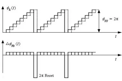
modulation as shown in Fig. 2, and △φFB is the
phase shift of ladder wave generated by the closed loop control system as shown in Fig. 3. From this equation, we know that the light intensity is a cosine function of phase shift. But, the output light intensity can not reflect the direction of rotation, and the system has a lower sensitivity. Therefore,
the system should be added a nonreciprocal ±π/2
phase offset through the square wave modulation. In the light path, we draw two alternative phases
with the values of π/2 and -π/2 into two lights in the
opposite directions. These two states have their own output light intensities respectively:
(
)
[
]
(
)
[
S FB]
d FB S d 2 sin 1 2 π cos 1
φ
φ
φ
φ
∆ + ∆ − = + ∆ + ∆ + = P P P (2)(
)
[
]
(
)
[
S FB]
d FB S d 1 sin 1 2 π cos 1
φ
φ
φ
φ
∆ + ∆ + = − ∆ + ∆ + = P P P (3)To do the different demodulation for Eq. 2 and Eq. 3, we obtain
(
S FB)
d 1
2− =−2 sin∆
φ
+∆φ
= [image:2.612.90.299.365.460.2]∆P P P P (4)
Figure 2. Schematic Diagram Of Square Wave Modulation.
Figure 3. Schematic Diagram Of Ladder Wave Modulation.
In the Eq. 4, the Sagnac phase shift △φS is
always approximately equal to △φFB and their
signs are opposite, because the added ladder wave
is used to counteract △φS. Therefore, △φS+△φFB
is always approximately equal to 0, then we have
Source Coupler Y-Waveguide Fiber Ring
Detector
A/D Digital D/A
Logic Square
Wave
[image:2.612.315.519.481.616.2](
)
( )
φ
φ
φ
φ
∆ − ≈ ∆ − = ∆ + ∆ − = ∆ d d FB S d 2 sin 2 sin 2 P P P P (5)Apparently, if △φFB can counteract completely
△φS, that is △φ=0, △P should be equal to zero. If
△P≠0, it is said that the nonreciprocal phase shift
generated by the ladder wave does not counteracts
the nonreciprocal phase shift caused by rotation yet.
This time, we can take △P as an error control
signal to change the step height of ladder wave
through the closed loop system to counteract △φ.
The additive nonreciprocal phase shift generated
by △P through the closed loop system is
P K∆ = ′
∆
φ
(6)where K is a scale coefficient to generate the
nonreciprocal phase shift through the closed loop
system. Then we have
(
)
(
)
(
PK)
P K P P P P d d d d d 1 2 1 2 2 2 2 − ∆ − = ∆ − ∆ − = ′ ∆ + ∆ − = ∆
φ
φ
φ
φ
φ
(7)If 2PdK=1, then △P1 =0, the control error of the
digital closed loop system is zero, it is indicated
that the closed loop reaches balance. If 2PdK≠1,
then the closed loop feedback control will be continued. After feedback controlling n times, the system will be in a state as following
(
)
nd d
n 2P 1 2PK P =− ∆ −
∆
φ
(8)From Eq. 8, we know that when 0< PdK <1/2,
the closed loop system can be monotonic convergence and will reach the balance gradually.
The condition 0< PdK <1/2 can be ensured by the
system design.
When the closed loop system reached the state of balance, the angular rate of rotation can be calculated by the equation as following and be measured by the FPGA module.
FB π 2
φ
λ
∆ − = LD CΩ (9)
where λis the wavelength of the optical source, LD
is the product of the length of optical fiber rings and the diameter of optical fiber ring.
3. CIRCUIT DESIGN OF DIGITAL CLOSED LOOP SYSTEM FOR FOG
A. System Frame Based on FPGA
The scheme used in this paper is the continuation of the traditional idea for designing the closed loop
control system of FOG, which consists of 6 components such as optical source generator, integrated light path, coupler, optical fiber ring, photoelectric detector and drive control circuit.
Structurally, we choose the integration solution of aluminum alloy material, i.e., the optical source control circuit board and the closed loop control circuit board are fixed in the body of optical fiber rings. We select the super luminiferous diode with a property of wide spectrum as the optical source and do constant power control in whole temperature
range (-40~60℃) using the optical source control
circuit board. The used optical fiber is the polarization maintaining fiber and the rings are winded by the quadrupole symmetrical winding pattern [12]. The total length of the fiber coil is about 650m.
[image:3.612.322.508.423.566.2]FPGA is a logic gate array, which is composed of many independent macrocells. These macrocells can be marked out some mutual non-interferential logic unites, which can work in parallel style. The signal exchange between the different logic unites can be realized through simple logical connections or some trigger levels [13]. This digital logic completely fits the demands of the application of the closed loop control system for FOG.
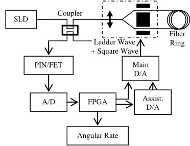
Figure 4. The Frame Of Closed Loop Control System Of FOG Based On FPGA
The FPGA based scheme is shown as in Fig. 4. We choose PIN/FET with bandwidth about 7~8MHz as the photoelectric detector. From the photoelectric detector to the post amplifier, all modules compose the digital closed loop control circuit, and they are integrated into a single PCB as a control circuit board of FOG. In the following sections, we will discuss the implementation of the control circuit board.
Coupler PIN/FET A/D Main D/A FPGA SLD Assist. D/A Angular Rate Ladder Wave + Square Wave
Fiber Ring
B. Preamplifier and A/D Module
[image:4.612.92.300.266.363.2]Since the optical signal is complicated relatively, after photoelectric converted, the electric signal come out from the detector has plentiful noises. As a signal picking up amplifier, the preamplifier needs to suppress the noises as clean as possible but must ensure its effective bandwidth. Therefore, we choose an operational amplifier with high rate, low excursion and low noise as the preamplifier. And we also design a cascaded directly coupled amplifier as shown in Fig. 5 to magnify the signal. Its gain should be adjusted according to the sensitivity of FOG and the precision of the closed loop control.
Figure 5. The Circuit Of Preamplifier.
After amplified, the signal should be converted from analog field into digital field to be processed conveniently. Due to existing of the white noise in the circuit, the A/D convertor should meet some requirements. If the LSB of A/D convertor is smaller than the standard deviation of the noise, then the sampling against the signal will be satisfied. According to the analysis, the ratio of the
standard deviation of the noise over π/2 offset
power is 2.83×10⁻³. For this order of magnitude, it
is enough to satisfy the requirements of circuit in the whole dynamic range when we just use a 12bit A/D to convert an analog signal to a digital signal. The digital integrator may bring the noise suppression like a low pass analog filter, but there is no long-term drift existing in the electronic circuit generally [9].
Additionally, we should consider the
eigenfrequency of system when doing A/D conversion. In our scheme, it is about 158kHz. In order to reduce the influence from noise to signal, the performance of A/D chip should ensure sampling 32 points at least in a semi-cycle (316kHz). At the same time, it should keep away from the peak of comb wave in favor of mean treatment. Therefore, the operating frequency of A/D sampling chip is at least 15MHz.
C. FPGA Logic Module
The main functions of FPGA include the integral filtering to the sampling signal, the digital generation of closed loop control, the digital generation of second closed loop control, the digital composition of square wave and ladder wave, the output of closed loop control and the output of angular rate.
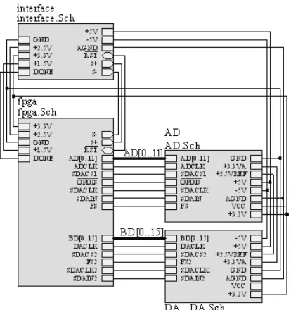
Its complete parallel processing enables FPGA to control the event of every time edge and process the relative data on micro point as well as hold the direction of data stream and process the data on macro point. The system connection diagram of FPGA [13] is shown as in Fig. 6. The digital logic in FPGA can be completed by software. Its detail will be described in the section 3.5.
Figure 6. The Connection Diagram Of FPGA.
D. D/A Module and Post Amplifier
The final part of the digital closed loop control system is the module for phase excursion control from the control voltage output to Y-waveguide. As a vital part of closed loop circuit, it should guarantee the integrality of signal strictly and satisfy the necessary regional linearity.
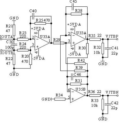
[image:4.612.315.522.291.511.2]having higher establishing times, which are far shorter than the transition time of a light going through the fiber rings.
[image:5.612.92.299.269.482.2]The basic connection idea is: the FPGA connects with and controls the main D/A and the assistant D/A. then take the output of the assistant D/A as a reference value and input it to the main D/A, form a closed loop circuit to control its gain and also provide a hardware for the second closed loop control. Finally, the output signal of the main D/A is magnified by two cascade operational amplifiers, and the result will be input into Y-waveguide with the difference method. The circuit of post amplifier is shown as in Fig. 7.
Figure 7. The Circuit Of Post Amplifier.
4. CONSIDERATIONS FOR HARDWARE DESIGN AND SAMPLE TEST
A. Component Selection
When applied to the practice, the system may meet quite atrocious circumstance condition and should work reliably even when the temperature is
from -40℃ to 60℃. Besides having compensation
by software, the system needs very good components to support it. A nice performance represented in the closed loop control board is the stabilization of hardware parameters in whole temperature range.
In our project, the temperature drift coefficients of all chips used in the system should be less than 10ppm, and the voltage reference should be less than 3ppm. The precisions of resistors used near the operational amplifier and determining the gain of
the amplifier should be 0.1%, and their temperature drift coefficients should be less than 25ppm.
The demands for the capacitors in the system are also rigorous. The functions of capacitors in the circuit can be classified into two types: the bypass capacitor for filtering and the blocking capacitor for separating the direct current. In order to ensure the stability of working signal, the power supply circuit should use the army grade tantalum capacitors with low ESR and ESL. The other stacked capacitors should select the high precision capacitors made by the material C0G or X7R.
B. Anti-jamming Design for PCB
An excellent PCB design is the crucial factor for the system working normally.
1) The basic principles for the PCB design
The basic principles for the PCB design are as follows:
a) Using multilayer board
The high frequency circuits usually have a high degree of integration and high density of layout. Using multilayer board is obligatory for the layout as well as an efficient measure for reducing the mutual interferences. In PCB design, choosing the number of layers reasonably for the power supply layer can decrease the size of PCB greatly. At the same time, the interim layer can be well used to set shield and it can make an advantageous condition for handy grounding. This measure can reduce the parasitic inductance effectively and shorten the transmission lengths for signals availably as well as depress the cross interference between signals greatly. Such performances improved will advantage the credible working of high frequency circuit. Some one proved that 4-layered board can reduce 20dB more noise than 2-layered board when using the same material. But more layers the board applied, more complicated manufacturing process adopted and higher cost will be.
b) Abstaining bended lead wires
The lead wires between the legs of components in a high frequency circuit should be straight but not bended. When the bended lead wires are
ineluctable, we should use 45 °fold line or arc
transition to reduce the emission of the high frequency signal and the coupling between the wires.
c) Lessening via holes
frequency circuit should be lessened. That is to say that via holes for connecting the components should be lessened. According to the test, a via hole can bring a 0.5pF distributed capacitance. Reducing via holes will enhance the rate of circuit remarkably.
d) Lessening via holes
The cross interference inducted by close parallel lead wires should be paid attention when arranging the wires in a high frequency circuit. If the parallel arrangement is unavoidable, laying a large area of ground on the back of the parallel lead wires should be considered to depress the cross interference greatly.
e) Ground surrounded processing
The ground surrounded measure should be used for the special signal wires or some local units such as the clock unit. It is also of benefit to the high rate system.
f) No loop ground, no current loop
The lead wires can not form a loop ground or a current loop. A high frequency decoupling capacitor should be set near every integrated circuit.
g) No loop ground, no current loop
The analog ground and digital ground connected to the common one need the high frequency choke links. When assembling the high frequency choke links, the high frequency ferrite beads with a lead passing through its central hole should be used.
2) General layout criterion of PCB board
On the basis of principles mentioned above, we determined the current general layout criterion for PCB board design.
a) Overall design
According to the requirements of structure of FOG in our project, PCB board is an anomalous roundness. Its diameter is 75mm. We design it using 6 layer PCB board. From the top to the bottom, they are upper signal layer, round layer, digital power supply layer, analog power supply layer, another ground layer and lower signal layer.
b) Power supply design
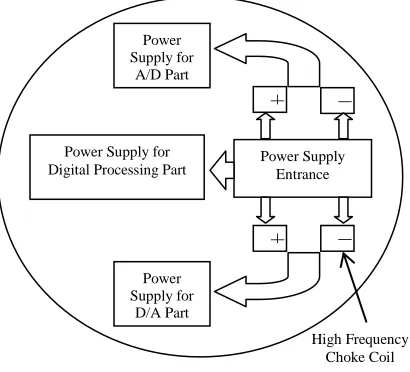
According to the requirements of system, the power supply interfaces of control board are split into two groups, i.e., A group (+5V, -5V and GND) and B group (+5V and GND), as shown in Fig. 8. They supply the powers for the main components and the output optocoupler on the control board respectively. In our project, we use decoupling design for every power entrance to the board and
connect with 47µF and 10µF tantalum capacitors in
turn to guarantee the calm of input power signal. And then, the signal of A group is split into tree routes. One of them connects to the input part of A/D through the high frequency ferrite bead. Another one for D/A. The third one links to the digital part of FPGA through the power supply chip. Before connected to their aim regions, three power supply units should be separated by the high frequency choke links and be filtered by a series filter networks, which are composed of the
tantalum capacitors with capacitances of 22µF and
10µF. Finally, a group of parallel capacitors of
0.1µF and 0.01µF should be connected to the
[image:6.612.315.520.312.498.2]nearest point from the power supplied chip. In order to ensure the calm of power supply, it should be transmitted in the form of surface through special layer to decrease the transfer impedance.
Figure 8.Layout Of Power Supply For PCB.
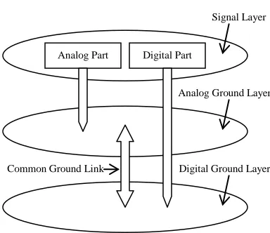
c) Grounding design
All earth wires have their impedances. The current must flow back to its source point like all
circuits. The current passing the efficient
impedance produced by the earth wire will make a potential drop, which will generate a ground loop current to form the ground loop interference. When two or more than two circuits use the same section of earth wire, a common impedance coupling will be produced. So, using the advantage of 6 layer board, our system builds two groups of large area ground to solve the problems of shield and decreasing the available impedance. This method can make the grounding current flowing back rapidly and enable the functional components to connect the earth in a shortest distance as soon as
Power Supply for
A/D Part
Power Supply for Digital Processing Part
Power Supply for
D/A Part
+ -
Power Supply Entrance
possible. The scheme of grounding design is shown as in Fig. 9.
Figure 9.Layout Of Ground For PCB.
d) Signal route design
According to the design principle, the lead wire of signal, which is susceptible to interference, should be short and thick. For example, the input signal wire of A/D convertor, the output signal wire of D/A convertor, the signal wire of reference source and so on, are such wires. Therefore, our project thinks over the routing manner of signal wires and selects the method of manual wiring, to insure having shortest distance of signal routing and to try our best to avoid via hole for signal routing. Additionally, using large area spreading coppers on two signal layers may reduce the impedance of ground wire, provide the shield for numerous signals and lesser current loop. It also achieved a good effect.
C. Sample Development and Experiment Test
We have developed some samples of FOG using the design method described in above sections and programming in FPGA with relevant algorithms. We also tested them using the performance items of scale factor and zero-bias through the experiments.
1) Scale factor test
The scale factor represents the proportional relation between the change of input rotation rate and the change of output of FOG. According to the measured input data and output data in the whole range of input rotation rates, we can use the least square method to calculate the slope of them. That is the scale factor.
Trough the experiment test, we obtained that the scale factor of our samples is about 0.0001154 deg•s/LSB, no matter the rotation direction of FOG.
2) Zero-bias test
The zero-bias is the output value of FOG when it is at zero input state.
Trough the experiment test, we knew that the zero-biases of all samples are all less than 0.075deg/h.
The experiments and tests show that the proposed method is efficient and valuable.
5. CONCLUSIONS
This paper presented a design method for the digital closed loop control system of FOG based on FPGA and developed some samples. Due to apply the twice closed loop technique, the zero-bias stability of FOG had been improved. After the test to the samples, the result data show that their zero-biases are all less than 0.075deg/h. Therefore, this method proposed in this paper is efficient and valuable. In addition, the agility of signal input and output interface of FPGA is convenient for hardware design. And, the digital signal processing by software in FPGA is also convenient for parameter adjustment in experiment. This technique can greatly shorten development period, improve the reliability of system and realize miniaturization of FOG.
The proposed method can be used in the fields of aviation, space, military affairs and so on. But the fluctuated zero-biases of FOG during warm up and at extreme temperatures limit its application areas. That is our research work to improve them in the future.
ACKNOWLEDGEMENTS
This research project was supported by the Key Disciplines of Shanghai Municipal Education Commission under Grant No. J51801, Shanghai, China and the Natural Sciences and Engineering Research Council of Canada (NSERC), Canada..
REFRENCES:
[1] L. Sun, and D. Z. Wang, “Latest development
of fiber optic gyroscope”, Spaceflight Control,
Vol. 21, No. 3, 2003, pp. 75-80.
[2] G. Sagnac, “L’éther lumineux démontré par l’
effet du vent relative d’ eth-er dans un
interferometer en rotation uniforme”,
Compte-rendus de l’Académie des Sciences, Vol. 95, 1913, pp. 708-710.
[3] K. Strandjord, “Performance improvements of
a polarization-rotating reso-nator fiber optic Analog Part Digital Part
Signal Layer
Common Ground Link
Analog Ground Layer
gyroscope”, SPIE, Vol. 1795, 1992, pp.314-320.
[4] K. Hotate, “Adjustment-free method to
eliminate the noise induced by the backscattering in an optical passive
ring-resonator gyro”, IEEE Photon.Technol. Lett.,
Vol. 2, No. 1, 1990, pp.109-112.
[5] K. Hotate, et al, “Grasp of the behavior of
lock-in phenomenon and a manner to overcome it lock-in
brillouin fiber optic gyro”, SPIE, Vol. 3541, pp.
57-65.
[6] F. Zarinetchi. et al, “Stimulated brillouin
fiber-optic gyroscope”, Opt. Lett., Vol. 16 , No. 4,
1991, pp. 229-231.
[7] G. A. Sanders, et al, “Fiber optic gyros for
space, Marine and Aviation Application”, SPIE,
Vol. 2837, 1996, pp. 53-71.
[8] W. Jin, Y. B. Liao, Z. P. Zhang, et al, “Guided
wave optical sensors: theories and techniques”,
Science Press, 1998.
[9] G. C. Zhang, and W. Wang, “Fiber optic
gyroscope”, National Defence Industry Press,
2002.
[10] X. W. Shu, “New fiber optic gyro of inertial
navigation system”, Laser & Infrared, Vol. 28,
No. 4, 1998, pp. 205-209.
[11] X. Y. Li, and Y. L. Hao, “Research on Digital
Closed Loop FOG Based on FPGA”, Journal
of Chinese Inertial Technology, Vol. 10, No. 2, 2002, pp. 39-43.
[12] J. K. Xie, Y. Q. Xuan, and J. Feng, “Electric
circuit”, Higher Education Press, 2004.
[13] S. Kilts, “Advanced FPGA Design”,