PARALLEL
DRUM
TYPE
-.'.-.. ~"~.~" -_ •... '.
DIGITAL EQUIPMENT CORPORATION • MAYNARD, MASSACHUSETTS
PARALLEL DRUM
TYPE 23
COpy NO.
0164
Th is manua I conta i ns proprietary i nformotion. It is prov ided to the cus-tomers of Digital Equipment Corporation to help them properly use and
maintain DEC equipment. Revealing the contents to any person or
organization for any other purpose is prohibited.
Copyright 1964
by
Digital Equipment CorporationPREFACE
This manual contains information on the principles of operation, and
procedures for installation, operation, programming, and
mainte-nance of the Digita! Equipment Corporation Type 23 Parallel Drum.
The parallel drum is designed for use as a data storage device to
aug-ment the main memory of a
PDP-l D
computing system. Section 1of this manual presents information of a general nature which is
applicable to the entire machine. Section 2 explains the principles
of operation of the parallel drum as a system and of each functional
element of the system. Sections 3 through 6 present information and
procedures which allow personnel to install, operate, program, and
maintain the equipment. Appendixes contain information on the
diagnostic program used to test the parallel drum, circuit data for
CONTENTS
Sect ion
Page
INTRODUCTION ...
1-1
Functional Description... . . .
1-1
Physical Description... . . .
1-2
Specifications ...
1-4
Symbols and Terminology ...
1-4
Circuit Blocks ...
1-8
S
i gna Is. . .
1 -8
Subscripts ... , . . .
1-10
Superscripts ...
1 -10
Other Notations ...
1 -1 0
Pertinent Documents ...
1 -10
Pub I ications ...
1 -10
Engineering Drawings ...
1 -11
Power Supply and Control ...
1-11
System Modules ...
1 -11
logic and Wiring ...
1-12
Section
3
4
6
CONTENTS (continued)
Drum Field Select ....•.••..•..•••.•...•...•.
Page
2-8
Pulsed Bus Transce iver .•••.••••••.•••....•... 2-9
In Buffer (IB) ...•.•.••...•..•....•... 2-9
Out Buffer (OB)
2-10
Parity Formation ...•...•.•••...••...•..
2-11
Parity Check ...•...•..••..•..•...•.
2-12
Data Writers .•..•.. . . • • • • • . • . • . • . . • . . . • . . . • . .
2-12
Data Readers .•.•....•..•...•...•...•••...•
2-13
Data Head Selection and Drum Memory .•..••...
2-13
Power Supply and Distribution ••••.•.•....•...
2-15
Read-Write Cycle...
2-18
Read On Iy Cyc Ie ...•...•..•••..•••.••••.•...•..
2-21
Write Only Cycle ..•...•.•••••••..••...
2-22
INTERFACE .•...•...•.•....•...•...
INSTALLATION AND OPERATION •..•••.•...•
Site Requirements ...••.•....•...•...
3-1
4-1
4-1
Signa
I
and Power Connections ....•..•••....•...•...•4-1
Controls and Indicators ...•...•...•.•.•.•.•...
4-2
Equipment Turn-On and Turn-Off .•...•...
4-6
PRO GRAMM I N G ....•...•...
5-1
MAINTENANCE . . . • . . .
6-1
Drum Housing Locations and Wiring . . .
6-2
Preventive Maintenance . . . . . .
6-5
Mechanical Checks ...•...•...
6-6
Power Supply Checks . . .
6-7
Timing Checks
6-7
CONTENTS (continued)
Sect ion
Page
Drum Sense Amplifier Checks ...
6-8
Index and Clock Head Spacing Checks. . .
6-8
Data Head Spac ing Checks. . .
6-9
Marginal Checks ...
6-11
Corrective Maintenance ...
6-14
Preliminary Investigation...
6-14
System Troubleshooting ...
0 0 0 0 0 0 0 0 0 • • • • 0 • 0 0 • 0 0 0 0 0 06-15
Diagnostic Program ...
0 0 0 0 • 0 • 0 • • • • 0 . 0 0 0 0 • • 0 0 0 0 0 • 06-15
Signal Tracing
0 . 0 0 • • 0 . 0 0 0 . 0 0 0 . 0 0 • • • 0 . 0 . 0 0 . 0 0 0 • • 06-16
Aggravation Tests
0 • • 0 • • 0 • 0 • 0 . 0 0 0 • 0 0 0 0 • • • • 0 0 0 • 0 • 0 •6-17
Circuit Troubleshooting.
0 0 0 0 0 0 • • 0 0 0 0 0 • 0 0 0 0 0 0 0 • • 0 0 0 0 0 0 06-17
Module Circuits
0 0 • • 0 • 0 • 0 0 • 0 0 0 0 0 0 0 0 0 • 0 0 0 0 0 0 0 0 0 0 0 •6-18
In-L ine Dynam ic Tests
0 0 • • 0 0 • 0 0 0 • 0 0 • 0 0 • 0 • • 0 0 0 0 • • •6-19
In-Line Marginal Tests .
0 0 . 0 • o . 0 0 . 0 0 • • • • • • • • • • • • 0 06-20
Static Bench Tests
0 0 0 0 0 • • 0 . 0 • • 0 . 0 0 . 0 . 0 • • • • • • • , • • •6-21
Dynamic Bench Tests
0 0 0 0 0 0 0 0 . 0 . 0 0 0 0 0 0 0 0 0 0 0 0 0 0 0 . 0 06-22
Repair
0 0 0 0 • 0 • 0 0 ' 0 0 • • 0 0 • • 0 0 . 0 0 0 • 0 0 0 0 0 0 0 0 0 0 0 • 0 0 • • • 0 0 •6-23
Validation Tests
o.
0 0 0 • • 0 0 0 . 0 0 0 . 0 0 0 0 . 0 0 0 0 • • • • 0 0 0 0 . 0 • • 06-23
Log Entry.
0 0 0 0 0 0 • 0 0 0 0 • 0 • • 0 0 • • 0 • 0 0 0 • • 0 • • 0 0 0 • 0 0 • • 0 0 • • 06-24
Appendix
TYPE 23 PARALLEL DRUM DIAGNOSTIC PROGRAM
0 0 0 . 0 . 0 0 0A 1-1
2
DRUM MODULES
0 • • • 0 0 0 0 0 0 • 0 0 0 0 0 0 0 0 . 0 0 0 0 0 • 0 0 • 0 • 0 • • 0 0 . 0 0A2-1
Type 1537 Drum Sense Amplifier
0 0 0 . o. 0 0 0 0 0 0 . 0 0 0 • • • 0 0 . 0 0 0 . .A2-1
Controls
0 • • 0 0 . 0 . 0 0 • • • 0 • • 0 0 . 0 0 . 0 . 0 0 0 0 0 0 0 0 0 . 0 0 • • 0 0 0 0 . 0A2-1
Input
o. 0 0 0 0 0 0 • • • • 0 • • • • • • 0 0 • • • ' 0 ' • • • • • • • • 0 . 0 . • • • • • • •A2-1
Output
0 • 0 • 0 • 0 • • 0 • • • • • 0 • 0 • • 0 • • 0 • 0 0 • • 0 • • • • • • • 0 0 • • • • • •A2-2
Power
0 . 0 0 . 0 0 . 0 • • • • • 0 0 • • • • • • • • 0 0 . 0 0 0 0 . 0 . 0 . 0 0 . . • • • • • •A2-2
Type 4518 Drum NRZ Writer
. 0 . 0 0 • 0 • • • • 0 • 0 • • 0 0 • • • • o • • 0 0 . • •A2-2
Input ... to • • • A2-3
Appendix
3
Table 3-1 3-2 3-3 3-4 4-1 5-16-1
A1-1
Al-2
Figure1-1
1-2 1-3 2-12-2
2-3 4-1CO NTE NTS:(
conti n u e
d)
Power . . . .
Page
A2-3
Type 4519 Drum Field Select... A2-3
Input . . . A2-4
Output ...•...•....•.... . . • . . . A2-4
Power ... A2-5
ENGINEERING DRAWINGS
TABLES
Inputs to Drum from PDP-1D ...•...
Outputs from Drum to PDP-1D ... .
Inputs to Drum from Memory Contro I ...••...
Outputs from Drum to Memory Control ... .
Controls and Indicators ...•...•...
I
nstruc t ions . . . . Maintenance Equipment ... .Diagnostic Program Switch Usage ... .
Error Printouts ... .
ILLUSTRATIONS
Typical Parallel Drum System Type 23 ... .
Component Locat ions ... .
Logic Symbols ...•.
Typical Recording and Playback Timing ...•...
Data Head Selection ... .
Drum Power C ircu it ... .
Indicator Panels ... .
ILLUSTRATIONS (continued)
Figure 6-1 6-2 6-3 6-4Pad Location •...•... Head Wiring ..•... Diode Board Wir i ng ...•... Read/Write Head Components ...•... A2-1
A2-2 A2-3
Type 1537 Logic Diagram Type 4518 Logic Diagram Type 4519 Logic Diagram
Drawing RS-728 RS-813 PW-D-23-0-8 RS-1000 RS-1l30 RS-1304 RS-1310 RS-1410 RS-1537 RS-1607 RS-1665 RS-1684 RS-4127 RS-4141 RS-4151 RS-4217 RS-4218 RS-4301 RS-4401
ENGINEERING DRAWINGS
ENGINEERING DRAWINGS (continued)
Drawing RS-4518 RS-4519 RS-4604 RS-6102 RS-6104 RS-6113 UML-D-23-0-7 UML-D-23-0-7 BD-D-23-0-17 TFD-D-23-0-1 BS-D-23-0-2 BS-D-23-0-3 BS-D-23-0-4 8S-D-23-0-5 BS-D-23-0-6 CL-A-23-0-13 CL-A-23-0-14 CL-A-23-0-15 CL-A-23-0-16Drum NRZ Writer ... .
Drum Field Select ... .
Pulse Amplifier ... .
Inverter
Inverter
Diode Unit ... .
Utilization Module List (Sheet 1) ... .
Util ization Module List (Sheet 2) ... .
Interface and Block Diagram ... .
Timing and Flow Diagram ... .
Control, Error Detection, Time Chain ... .
In Out Buffers and Pu Ised Bus Transceiver ... .
Sense Amplifiers, Write Amplifiers, and Parity ... .
Read/Write Field Buffers and Field Select ... .
Core Location, Drum Counter, Initial Location
and Word Counter ... .
Reader Output from Drum Housing (2CJ6) ... .
Field Select Input to Drum Housing (2CJ4) ... .
Writer Input to Drum Housing (2CJ3) ... .
PDP-l D Interface With Drum (2CJ1) ... .
Figure 1-1 Typical Parallel Drum System Type 23
[image:13.613.89.547.55.683.2]SECTION 1
INTRODUCTION
The Digital Equipment Corporation (DEC) Type 23 Parallel Drum serves as auxiliary data
stor-age for the core memory of a Programmed Data Processor - 1 D and faci I itates time shared use
of the computer. Information in the computer can be stored (written) in the parallel drum and
retrieved {readL or can be simultaneously read and written in a swap or data exchange. The
drum contains 32 fields; each field is capable of storing 4096 words. Each word contains 18
information bits and an odd parity bit. The parity bit is generated within the drum during
write operations and is checked during read operations to provide a means of check ing the
18-bit information transfer between the drum and the computer. All transfers are completely
automatic as controlled by the computer program. Transfers of from 1 to 4096 words can be
executed at a rate of 8.5 microseconds per word, exclusive of set-up and access time.
Trans-fer or exchange of 4096 words is accompl ished in approximately 35 mi II iseconds.
FUNCTIONAL DESCRIPTION
The basic functions of the Type 23 Para Ilel Drum are data storage and retrieva I, computer
core memory address control, drum track and field selection, data request and transfer control,
error checking, and power supply and distribution. Functional operation of the machine is
initiated by receipt of lOT pulses from the computer. Three computer instructions produce
all of the lOT pulses required to enact a transfer between the computer memory control and
the para lie
I
drum, regardI
ess of the word I ength of the transfer.A power supply and distribution network within the parallel drum produces and controls the
operating voltages required by all circuits of the machine. One source of external ac power
is required to energize the machine; control of this source within the machine can be exercised
loca Ily or remotely at the computer.
In response to lOT pulses from the computer the parallel drum receives the drum address from
the computer, receives the number of words to be transferred and the read/write/exchange
The transfer is then enacted in either the program interrupt or sequence break computer modes.
Eighteen iJ;ts are simultaneously read from or written on the surface of the continually rotating
drum and are transferred to or from the computer memory control element by means of a
bi-directional pulse bus transceiver. During a write operation, a parity bit is generated within
the drum for each word received from the computer so that 19- bit words are written on the drum
surface. In reading data from the drum, the parity of the word is checked to assure proper
transmission. Error circuits in the machine check for parity error during read cycles and check
for data transm iss ion timing during both read and write cycles. If bits are picked up or dropped
out, if data received from the computer is late during a write cycle, or
if
data is late in beingstored in the computer core memory during a read cycle, an error flag is set and a signal is
sent to the computer and the transfer is ha Ited. The computer program can interrogate the
drum to determ ine the error status and the type of error detected when the error flag is set.
Control circuits within the parallel drum initiate the computer break status for the transfer,
indicate the completion of a transfer by means of a flag, and signal the detection of an error,
in addition to performing the normal internal control operations.
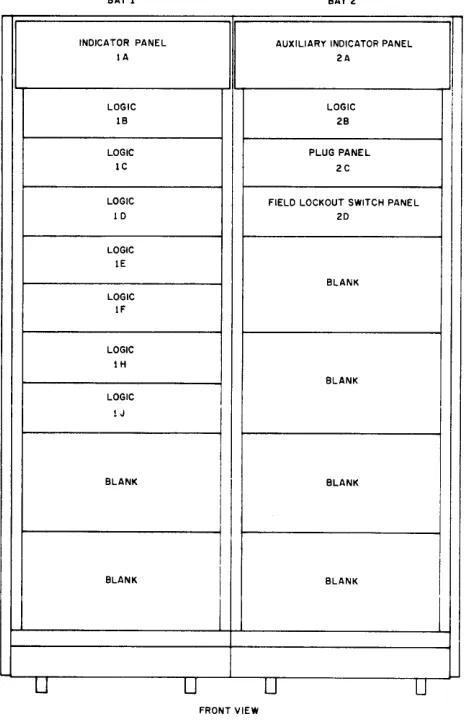
PHYSICAL DESCRIPTION
The parallel drum is constructed of two standard DEC computer cabinets bolted together to form
a cabinet 60-1/8 inches high, 47 inches wide, and 27-1/16 inches deep. All indicators and
the power control switch are located on panels at the front of the machine. Additional controls,
used to inhibit writing in each of the drum fields independently and to force an incorrect parity
bit as a check of the error circuits, are located on a switch panel inside the front doors of the
right-hand cabinet. Eight casters allow mobility of the 900-pound machine.
Each cabinet is constructed of a welded steel frame covered with sheet steel. Double rear
doors are held closed by magnetic latches. A full-width plenum door provides mounting for
the Type 813 Power Control and two Type 728 Power Supplies inside the double rear doors.
The plenum doors are latched by a spring-loaded pin at the top. Plug panels, which accept
the signal cables from the computer, and module mounting panels are located in the front of
the mach ine with the wiring side outward. A fan mounted in the bottom of each cabinet draws
cooling air through a dust filter in the bottom, passes it over the electronic components, and
exhausts it through louvered panels and openings in the cabinet.
A coordinate system is used to locate cabinets, module mounting panels, modules and signal
cable connectors, and terminals within the machine. As viewed from the front, cabinet 1 is
on the left and cabinet 2 is on the right. Each 5-1/4 inch position on the front of the cabinet
is assigned a capital letter, beginning with A at the top. Modules are numbered from 1 through
25 from left to right in a mounting panel, as ·viewed from the wiring side. Connectors on a
plug panel are numbered from 1 through 6, from left to right as viewed from the front of the
machine. Blank module and connector locations are numbered. Terminals on a module
con-nector are designated by capita I letters from top to bottom. The letters G, I,
0,
and Q areomitted from module and terminal designations. Therefore, 1C06J is in cabinet one
(1),
thethird component location from the top (C), the sixth module from the left (06), and the ninth
terminal from the top of the module
(J).
Components mounted on the plenum door are notidentified by location. Figure 1-2 indicates the location of components within the parallel
drum.
BAY 1 BAY 2
INDICATOR PANEL AUXILIARY INDICATOR PANEL
IA 2A
LOGIC LOGIC
IB 2B
LOGIC PLUG PANEL
lC 2C
LOGIC FIELD LOCKOUT SWITCH PANEL
J 0 20
LOGIC IE
BLANK LOGIC
IF
LOGIC IH
BLANK LOGIC
! J
BLANK
I
BLANK
I
I
BLANK
I
BLANK
I
U
u
U UFRONT VIEW
[image:16.612.190.422.345.706.2]Dimensions
Service Clearances
Weight
Power Required
Power Dissipation
Power Contro
I
Po i ntInitia
I
Starting DelayHeat Dissipation
Signal Cables
Temperature
Drum Motor
Magnetic Head Interference
Wri te Current
Read Current
Pulse Repetition Rate
Drum Revolution Time
SPECIFICATIONS
47 inches wide, 27-1/16 inches deep, 69-1/8 inches high
8-3/4 inches in front 14-7/8 inches in back
1000 pounds
115 volts, 60 cycles, single phase, 10-ampere starti ng current, 9-amperes runn i ng current
750 watts
loca I or remote (computer)
20 minutes
2558 BTU/Hours
Three 50-wire shielded and one 18-wire coaxial
32 to 105 degrees F operating range
115 volts, single phase, 4-pole induction capacitor start and run
Maximum interchannel read cross talk at least 25 db below nominal signal level. Maximum noise in any channel at least 25 db below nominal signal level.
1.75 amperes at - 14 volts for 19 heads
20 mill iamperes at + 4 vo
I
ts for 19 heads8.5 microseconds
35 mill iseconds
SYMBOLS AND TERMINOLOGY
Engineering drawing numbers for this equipment contain five pieces of information, separated
by hyphens. Read from left to right these bits of information are a 2-letter code specifying
the type of drawing, a 1-letter code specifying the size of the drawing, the type number of
the equipment: the manufacturing series of the equipment, and a 2-digit number specifying
the number of a drawing within a particular series. The drawing type codes are:
a. BS, block schematic or logic diagram
b. el, cable list
c. PW, power wiring
d. RS, repiacement schematic
e. TFD, timing and flow diagram
f.
UML, util ization modu Ie listg. WD, wiring diagram
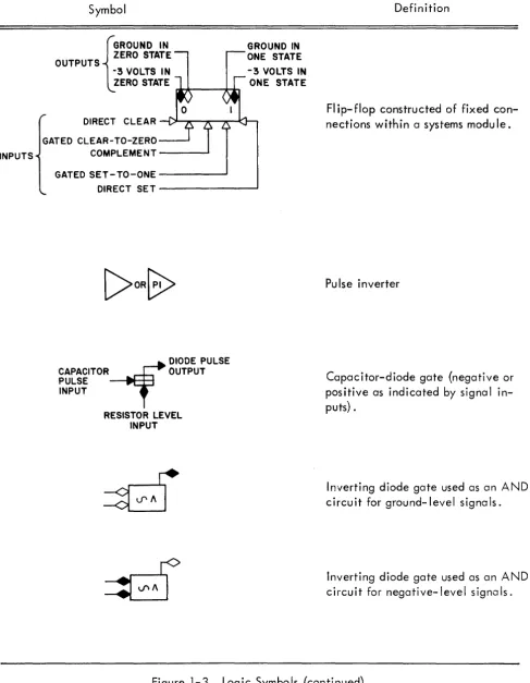
Symbols used on engineering drawings to represent basic logic circu its are defined in Figure 1-3.
SET-TO-ONE
Symbol
---I>
•
COLLECTOR
BASE~ORD
EMITTER
CLEAR-TO-ZERO
Definition
Standard DEC Positive Pulse or posi-tive-going transition
Standard DEC Negative Pulse or negative-going transition
Standard DEC Ground Level signal
Standard DEC Negative Level (- 3 vdc signa I)
Load resistor clamped at - 3 vdc
Transistor inverter
Bistabl e mul tivibrator (fl ip-flop
constructed of two cross-coupled inverters.
[image:18.617.81.550.248.714.2]Symbol
OUTPUTS
t
GROUND INZERO STATE
-3 VOLTS IN ZERO STATE
~~--+-r.
GROUND IN ONE STATE -3 VOLTS IN
ONE STATE
DIRECT CLEAR - .. r~ _ _ _ _ ~~...,
GATED CLEAR-TO-ZERO
INPUTS COMPLEMENT - - - - '
GATEDSET-TO-ONE---~
DIRECT SET - - - '
DIODE PULSE CAPACITOR-f OUTPUT PULSE
INPUT
RESISTOR LEVEL INPUT
Definition
FI ip-flop constructed of fixed con-nections within a systems modu Ie.
Pulse inverter
Capacitor-diode gate (negative or positive as indicated by signal In-puts) .
Inverting diode gate used as an AND circuit for ground-level signals.
Inverting diode gate used as an AND circuit for negative-level signa Is.
Figure 1-3 Logic Symbols (continued)
[image:19.617.61.549.73.701.2]Symbol
Figure 1-3
Definition
Inverting diode gate used as an OR circuit for negative-level signa Is.
Inverting diode gate used as an OR circuit for ground-level signa Is.
Diode OR and AND circuit followed by inverter.
Inverting diode gate used to trigger a pulse amplifier.
[image:20.618.71.552.66.710.2]Abbreviations and conversions used in this manual, on the engineering drawings, or on panel
markings are defined in the following list.
ACT
DBA SYNC
DC
DCl
DRA SYNC
ERROR SYNC
Il
PA
PE
PI
RFB
RQ
SA
TRA
TRANS ERROR
WC
WFB
ACT
ADRS ACK
DBA
DC=ll
DC => 10 STROBE
DCl
DCT CLEAR
DCT DISABLE
Circuit Blocks
Active fl ip-flop
Drum break address fl ip-flop
Drum counter
Drum core location
Drum read address fl ip-flop
Error synchronization fl ip- flop
Initio I location
Pulse amplifier circuit
Pari ty error fl ip- flop
Pulse inverter circuit
Read field buffer
Request fl ip-flop
Sense amplifier {reader}
Transfer status flip-flop
Transfer error fl ip-flop
Word counter
Write field buffer
Signa Is
Active fl ip-flop or level
Ad
I ,I
I ,cress aCKnow eage pu Ise
Drum break address instruction or fl ip-flop
level indicating C{DC} = C(ll)
Pulse which strobes C(DC) => C(lO)
Drum core location instruction or register
Drum control clear pulse
Drum control disable level
DIA
DRA
DWC
IB
10
lOB ADRS ACK
MA
OB
PBT
PWR ClR
MB
RD RS
RD REQ or RD RQ
RFBH
RFBl
RQ
RQB
SA
SBS RETURN
TE or TR ER
TP WC WFBH WFBl WFD WFlO
WR REQ or WR RQ
WR WS
Signa Is (conti nued)
Drum initial address instruction
Drum request address instruction or fl ip-flop
Drum word counter instruction
In buffer register or level
Input-output register or level
Input-output buffered address acknowledge pulse
Memory address register or levels from the DCl to this register
Out buffer register or levels
Pu Ised bus transceiver
Power clear pulse
Memory buffer register or input-output levels of the PBT
Read restart pu Ise
Read request level
Read field buffer high digit level
Read field buffer low digit level
Request level
Request level buffered
Sense ampl ifier circuit (reader) or pu Ises
Sequence break signal return pulse
Transfer error level
Timing pulse
Word counter register or level
Write field buffer high digit level
Write field buffer low digit level
Write field disable buffer
Write field lockout switch or level
Write request leve I
o
through 6o
V
-¥-A
C(A)
A
=>
BC(A)O_5
=>
C(B) 6- 11Subscripts
Individual bit numbers of a register,
counter I or fl ip-flops
Superscripts
Signal condition for flip-flop binary 1 status
Signal condition for flip-flop binary 0 status
Other Notations
Inclusive OR
Exclusive OR
AND
Contents of register A
A replaces B or B is set to A
The contents of bits 6 through 11 of register B are set to correspond with the contents of bits 0 through 5 of register A.
PERTINENT DOCUMENTS
Publ ications
The following DEC documents serve as source materia
I
and complement the information inthis manua
I:
a. Digital Modules Catalog, A-705. This book presents information pertaining to
the function and specifications for the basic systems modules and accessories comprising
the Type 23 Parallel Drum.
b. Silicon Modules Catalog C-6000. Information on the function and specifications
for the 6000 series system modules is contained in this book.
c. PDP-1 Handbook, F- 15. Programming information for the Programmed Data
Pro-cessor - 1 is presented in this document.
d. PD P - 1 Supplements, F - 15 (1 D - 45) and F - 15 (1 D - 48). These documents
des-• I . I • I . . • • " I . . I n~ n , I I • • . • I nf"\ n 1 f"\
Crtbe rne speCial InstrUCTions aooeo TO Tne rlJr- I wnen usea In a Typical rur- i u
configuration, such as that at Bolt Beranek ard Newman, Inc. (45) and at Stanford
University (48).
e. PDP- 1 Maintenance Manual, F- 17. Installation, operation, and maintenance
of the standard PDP- 1 and its central processor options are covered in this manual.
f.
Parallel Drum Diagnostic Program Tape, DEC -1 -
137 - M.A
perforated- papertape and program resume of a routine which tests the data reading, writing, and
sw(]pping operations of the drum system.
Eng i neer i ng Draw i ngs
Engineering drawings in the following list are reproduced in Appendix 3 of this manual as an
aid to understanding and maintaining the Type 23 Parallel Drum.
A
complete set of formalengineering drawings is supplied separately with each system. Should any discrepancy exist
between the drawings in this manual and those supplied with the equipment, assume the formal
drawings to be correct.
Power Supply and Control
Power Supply ..•• 0 • o . 0 0 0 . 0 . o . 0 • • 0 0 • • 0 • • 0 o . 0 • • • • • o • • • 0 0 0 0 o . 0 0 0 • o . RS-728
Power Con trol 0 • • • • • • • • • • • • • • • • • • 0 • 0 • • • • • 0 • • 0 0 • • • 0 • • • • • • • 0 • • • • • 0 RS -813
AC-DC Wi ring •••• 0 • 0 • • • • • • • • • • • • • • • • • • • • • • • • • • • • • • 0 • • • • o . PW -D -23 -0-8
System Modules
Clamped Load Resistors RS-1000
Three-Bit Parity Circuit. 0 . 0 0 . 0 0 . 0 0 . 0 . 0 . 0 . 0 0 0 • • • • • 0 . 0 o. 0 0 0 . 0 . 0 . 0 . RS-1130
Delay (monostable multivibrator) .•••.• 0 • • • • • • • • • • • 0 . 0 . 0 0 • • 0 0 . 0 0 0 . RS-1304
Delay Line. 0 0 0 • • • 0 . 0 . 0 0 0 0 . 0 0 . 0 0 0 • • 0 0 • • 0 • • • 0 • • 0 • • • 0 0 0 • • • 0 • • • • • • RS-1310
System Modules (continued)
Pu Ise Ampl i fi e r ..
0 • • • 0 • • • • • • • • 0 • • 0 • 0 • 0 • 0 • • • • • • 0 • • • 0 • • 0 • 0 • • • • • • _RS -1607
Pulsed Bus Transceiver .•..
0 • • 0 0 . 0 • • 0 0 . 0 0 . 0 0 0 0 0 0 . 0 0 0 0 0 . 0 0 0 0 0 0 0 0 0 0RS-1665
Bus Driver ...•...•...•...•... RS -1684Capac i tor-Diode-Inverter
0 0 0 0 0 0 0 0 0 0 0 0 0 0 0 0 0 0 0 0 0 0 0 0 0 0 0 0 0 0 0 _ 0 0 0 • 0 0 0 0RS -4127
Diode Unit ... $ • • • • • • • • • • • • • • RS-4141Binary-to-Octal Decoder
0 0 0 0 0 0 0 0 0 0 0 0 0 0 0 0 0 0 0 0 0 0 0 0 0 0 0 0 0 0 . 0 0 0 0 0 0 0 00RS-4151
Four-Bit Counter
0 0 0 0 0 0 0 0 0 0 0 0 0 0 0 0 0 0 0 0 0 0 0 0 0 0 0 • • • • • 0 . 0 . 0 • • • 0 0 • • 0 0 0RS-4217
Quadruple Flip-Flop
0 0 0 . 0 0 0 0 0 . 0 0 0 0 0 0 . 0 0 0 0 0 0 0 0 0 . 0 0 0 • • • 0 0 0 . 0 . 0 . 0 . 0RS-4218
Del a
y •.•••••••••••••••••.••••••.•••••• • • • • • • • • • • • . • • • • • • • • ••• RS -43 0 1Clock ...
RS-MOl
Drum
NRZ
Writer.. .. . .. . ... ... .. . .. . .. .. . .. . .. .. . .. . ... RS-4518Drum Field Select
0 0 0 0 0 0 0 0 0 0 0 0 • • 0 0 0 0 • • 0 0 . o • • o • • • 0 0 0 . 0 0 0 0 0 0 . 0 0 0 0 0RS-4519
Pulse Ampl ifier ... . .. . .. .• . .. . .. . . . .. . .. .. . .. . .. .. . .. . . . .. .. RS-4604Inverter. . . .. .. . . .. . .. .. . .. . .. .. . .. . . . .. . . .. . . . .. . ... RS-6102
Inverter.. . . . .. . .. . . .. . . . .. . .. . .. .. . .. . .. .. . .. . .. .. . .. . ... RS-6104
Diode Unit.. . .. . . .. . . . .. . .. . . . .. . .. .. . .. . .. .. . .. . .. . . ... RS-6113
Util ization Module List.
0 0 0 0 0 0 0 0 • 0 . 0o.
0 0 0 0 0 • • 0 • 0 0 . 0 0 • 0 0 0 0UML-D-23-0-7
Logic and Wiring
Interface and Block Diagram
0 0 0 • 0 0 • • 0 • 0 • 0 0 0 0 0 • 0 0 0 • 0 0 0 0 • • •BD -0 -23
-0-17
Timing and Flow Diagram
0 0 0 0 0 . 0 0 • • 0 0 0 0 0 . 0 0 0 • • 0 • • • 0 0 0 . o.TFD-D-23-0-1
Control, Error Detection Ti me Cha in
0 0 • 0 0 0 0 • • 0 0 0 • 0 0 • • 0 • 0 0BS -D -23 -0-2
In Out Buffers and Pulsed Bus Transceiver.
0 0 . 0 • 0 0 • 0 0 0 0 0 o . 0 0 0BS-D-23-0-3
Sense Amplifiers, Write Amplifiers, and Parity
0 . ' 0 • • 0 0 0 0 . 0 0 0BS-D-23-0-4
Read/Write
FieldBuffers and Field Select
0 0 0 0 0 . 0 . 0 0 0 0 . . .BS-D-23-0-5
Core Location, Drum Counter, In itia I Location and
Word Counter
0 0 0 • • 0 0 • • • 0 0 . 0 0 0 0 0 . 0 • •BS-D-23-0-6
Reader Output from Drum Housing (2CJ6) ...
0 • 0 0 0 • • 0 0 0 0 • • o .CL-A ... 23-0-13
Field Select Input to Drum Housing (2CJ4)
0 . 0 0 0 . 0 . 0 0 . 0 0 0 0 0CL-A-23-0-14
Writer Input to Drum Housing (2CJ3)
o. o.
0 • • • 0 • • • 0 0 0 • 0 • 0 0 _CL-A-23-0-15
PDP-1 D Interface With Drum (2CJ1)
o. 0 • 0 • • 0 0 0 • • • 0 0 0 0 0 • 0 ' 0CL-A-23-0-16
SECTION 2
PRINCIPLES OF OPERATION
RECORDING AND PLAYBACK TECHNIQUE
The Type 23 Parallel Drum utilizes return-to-bias recording techniques which lend themselves
to the simultaneous read and write, or exchange, operation required of the drum. In each bit
cell the new information to be written in a field is available just before the information is to
be read from another field. Because of noise considerations, the read strobe must precede the
write strobe. The effective advance of the read strobe over the write strobe, which previously
wrote the information to be read, is possible because of the fringing of flux ahead of the data
head gap. Before a transfer begins the read and write head select circuits are enabled. At the
beginning of a transfer bias current is applied to the write-selected heads so that all transients
occur and damp out before the occurrence of the read strobe. In a data exchange operation
the read strobe is followed by the write strobe, and write noise is induced in the sense
ampli-fier. This noise is commonly of greater amplitude than the read signal; however, this noise
damps out before the next read strobe occurs. The read and write current waveforms and the
timing of the read strobe and write strobe are indicated in Figure 2-1 .
BLOCK DIAGRAM DISCUSSION
Functional elements of the parallel drum are shown on engineering drawing BD-D-23-0-17.
This drawing indicates all signals which flow between the elements of the drum, and between
drum elements and the PDP-1 D and the Memory Control. The only signals which are not
in--dicated are the phase signals out of the timing element which go to all logical blocks and the
operating voltages which also are supplied to all elements from the power supply and distribution
element. Detailed information on each of the functional blocks is indicated in block schematic
engineering drawings BS-D-23-0-2 through
6,
and complete information transfer flow in timingoperations is indicated in engineering drawing TFD-D-23-0- 1. The distribution and wiring of
the power circuits within the parallel drum are indicated in engineering drawing PW-D-23-0-S.
As reference is made to these drawings in the following text, only the final portion of the
tv
1
tv
TIMING
WRITE ENABLE
WRITE STROBE
READ STROBE (PRECEDES WRITE
STROBE BY a.lpSEC)
IN BUFFER (EXAMPLE OF BIT
X IN FOUR SUBSEQUENT WORD LOCATIONS)
WRITE CURRENT FOR ONE HEAD 0
(WRITE FIELD Y)
READ HEAD VOLTAGE (READ FIELD Z) (1,0,0,1, PREVIOUSLY
WRITTEN IN FOUR SUBSEQUENT LOCATIONS)
GROUND -SLICE OUTPUT
LOAD
- 3 - + - - - - '
CLEAR
0
S A OUTPUT - + - - - - " " " " \ 1
"'---If---If---i---_I ....
---t---I I I I I I I TIME pSEC 0 2 3 4 5 6 7 80
Figure .2-1
I I I I I I I
2 3 4 5 6 7 80
I I I I I I I
2 3 4 5 6 7 80
Typical Recording and Playback Timing
[image:27.795.60.718.57.542.2]on the drawing. These coordinates are A through D from top to bottom and 1 through 8 from left
to right; so zone A 1 is in the upper left hand corner, and zone D8 is in the lower right hand
corner. Note that register bits are numbered to correspond with the computer register bits to
which they transfer data. Therefore, most register bits are numbered so that the least
signifi-cant bit is designated bit 17.
Index and Clock Readers
In addition to the normal data tracks recorded on the drum surface, two tracks provide timing
information used in the control of normal drum operations. These two tracks are the index and
the clock tracks. The information on these tracks is prerecorded and is read from the index
track by the Type 1537 Drum Sense Amplifier module at location 286 and is read from the
clock track by the Type 1537 module at location 2B5. One index bit is recorded on the
sur-face of the drum to indicate the starting address of all words written on the data tracks. The
output signa I level from the index sense ampl ifier initiates operation of a Type 1304 Delay
modu Ie whose negative pu Ise output clears the drum counter and signifies the start of each
new drum cycle. The delay is provided to allow adjustment of the timing relationship of an
index pulse so that it occurs exactly in the center of the time between the first and last clock
pulse. The output of the clock sense amplifier initiates operation of a Type 1410 Pulse
Gener-ator module at location 2B4 to produce a standard DEC 70-nanosecond clock pulse which
ini-tiates operation of the timing element and controls the timing of all operations in the parallel
drum. There are 4096 clock bits recorded around the surface of the drum; each clock pu Ise
signifies a data bit cell location. Engineering drawing 4 contains this logic in the lower
left hand corner.
Timing
The timing element consists of a timing chain generator composed of delay lines, delays, and
pulse amplifiers which produce the read strobe, write strobe, phase 1, phase
2,
phase 3, phase4, and phase A pulses. The timing chain is initiated by receipt of a clock pulse from the clock
reader element. Transistor gating circuits allow generation of the read strobe signal only when
the drum is in the read mode and in the active status. The phase 1 signal can be generated
signals are enabled only when the drum is in the active status. The phase 4 and phase A pulses
cannot be disabled. In addition to these pulses the timing element produces the DCT disable
signal, which is a constant - 3 vdc level produced by clamped load resistors. This level is used
wherever constant enabling or disabling - 3 vdc levels are required. The phase 3 signal initiates
operation of the Type 4604 Pulse Ampl ifier in location 1 F4 whose output is the write restart
0NR RS) signal, which is supplied to the memory control and to the parity formation element.
Control
The control element contains nine flip-flops (TRA, RQ, ACT, ERROR SYNC, TRANS ERROR,
PE, DRA SYNC, DBA SYNC, and busy) which determine and control the status of the parallel
drum. This element is shown on engineering drawing 2, above the timing element and the
parity check element. When power is initially applied to the parallel drum, the Type 4401
Clock at location 1 F2 is enabled by a ground level suppl ied to terminal B and produces repeated
power clear pulses. The power clear pulses clear the parity formation element and various
registers of parallel drum in addition to all of the flip-flops in the control element. After an
initial delay period of approximately 30 seconds, the normally closed contacts of time-delay
relay D2 of the Type 813 Power Control open to remove the ground potential from the
inte-grating circuit at the input of the clock module to disable it.
The nine control flip-flops are also cleared by receipt of the DIA 7-4 command pulse, which
is received during the first instruction in the initializing sequence. All of the flip-flops except
the busy fl ip- flop are set to one or c
I
eared to zero by the phase A pu Ise, as a function of thecondition of level signals suppl ied to capacitor-diode gates. The busy fl ip-flop is constructed
of two cross-coupl ed inverters wh i ch function as an unbuffered fl ip- flop. Th is fl ip- flop is
cleared to zero by power clear pulses, the DIA 7-4 pulse, or a sequence break signal return
and is set to
1
by theDel 10-4
puise. The function of the other ft ip-flops can be determ inedby the control signal or lOT pulse inputs required to set or clear them.
Drum Counter (DC)
The DC is a 12-bit counter which keeps track of the angular position of the continually
ro-tating drum. This register is cleared by the index pulse provided by the index reader, and is incremented
by one by each phase A pu Ise. Both the 1 and 0 outputs from each bi t of th is reg ister are
suppl ied to a comparCltor so that a data transfer is requested when the drum reaches the
posi-tion, or drum address, set into the initial location register. The contents of this register can
also be set (read) into the PDP-1 D
10
register to monitor the angular position of the drum.The logic circuits for the DC are shown on zone B of engineering drawing 6.
Initial Location Register (lL)
The IL is a simple set-and-reset 12-bit register which is used to store the initial address or first
address at which the drum is to read or write. During either a DIA or DBA instruction, the
register is cleared at computer 7 time and is set to the address contained in
10
bits 6 through17 at computer 10 time. Both the 1 and 0 outputs from this register are continuaiiy supplied to
a comparator for comparison with the contents of the DC. This register is shown on zone C of
engineering drawing 6.
Comparator
The comparator, shown on zone B8 and C8 of eng ineering drawing 6, continua lIy mon itors the
contents of the DC and the IL. The circuit provides a bit-by-bit exclusive OR comparison of
the contents of these two registers and supplies the negative DC = IL signal to the control
cuit when the two registers contain the same drum address. This signal causes the control
cir-cuit to set the request flip-flop to the 1 status if the transfer flip-flop is also in the 1 status.
The output of this flip-flop is then supplied to memory control to request a transfer. When using
the DBA instruction, the DC = IL signal also initiates generation of the sequence break signal
return pulse which is supplied to the computer to initiate a transfer through the sequence break
mode, and clears the busy flip-flop.
Word Counter (WC)
The WC is a 12-bit binary counter which controls the number of words transferred during any
drum operation. The WC logic is shown on zone A of engineering drawing 6. During a DWC
instruction, the contents of the computer
10
register are set into the write control, the writefield buffer, and the word counter. At this time the
10
register information contained in bitsbe enabled. The contents of bits 6 through 17 of the
10
register specify the number of words to be transferred. The l's complement of the contents of bits 6 through 17 of the computer10
register is set into the contents of the word counter at computer time 10 (the WC is clearedat computer 7 time by the DWC instruction). During the ensuing DCl instruction, the contents
of the WC are incremented by one by the DCl 7 - 4 lOT pulse; therefore when the transfer is
initiated by the DCl instruction, the word counter holds the 2's complement of the number of
words to be transferred. As each word is transferred, the wri te strobe pu Ise increments the
contents of the WC. The write strobe pulse is used for this operation since both reading and
writing have been completed at the current drum address when this pulse occurs. Therefore,
when the specified number of words have been transferred, the most significant bit of the WC
changes from the 1 state to the 0 state. The
WC~
signal clears the request flip-flop in thecontrol element to signify to the computer that the transfer is complete.
Drum Core location Counter (DCl)
The DCl is a 16-bit register which specifies the computer core memory address to or from which
the next word is to be transferred. The contents of the DCl are sampled by the memory control
and set into the contents of the core memory address register for each word of a transfer. Bits
6 through 17 of the DCl function as a setable counter which is automatically incremented by
receipt of the lOB address acknowledge pulse from memory control. Bits 2 through 5 of the
DCl are always transferred into the memory address register as they are set by computer
10
register bits during the DCl instruction program initialization. Bits 2 and 3 specify one of
four 16, 384-word memory banks to be used for the transfer,and bits 4 and 5 specify one of
four 4096-word memory modules within the memory bank. Therefore, the parallel drum is
capable of operating with a computer containing 65,536 words of core memory with a maximum
transfer word length of 4096 words. The Del is shown on zones C and D of engineering
drawing 6.
Before normal drum transfer operations, the DCl is cleared by the power clear pulses. During
the third lOT instruction of the drum initialization program, the DCl instruction clears the
DCl at computer 7 time and sets the contents of the
10
register into the contents of the DClat computer 10 time. Bits
6
through 17 of the DCl are incremented at the comp letion of eachword transfer by the lOB address acknowledge pulse. All outputs from the DCl to the memory
control are buffered by a non-inverting Type 1684 Bus Driver module.
Read Control and Read Field Buffer (RFB)
Read control is a single flip-flop which determines if reading from the drum is enabled or
dis-abled during any data transfer. The flip-flop is set to the 1 status (to enable reading) or to
the 0 status (to disable reading) by the contents of
10
register bit 0 during the first instructionof the drum initialization program (DIA or DBA instruction). The 0 output from the read
flip-flop is buffered by circuit HJ on the Type 6102 Inverter module at location 1 F22 to produce
the read buffered (B) signal. This buffered signal, supplied to the timing element and to the
control element, is a - 3 vdc level when the flip-flop is in the 0 status and is a ground level
signal when the flip-flop is in the
1
status. When the read flip-flop is in the1
status,transis-tor gating circuits in the timing element are enabled to produce the read strobe pulse, thereby
allowing read operations to take place. When the read flip-flop is in the 1 status, the read
buffer signal supplies one input to the UVW circuit of the Type 6113 Diode Unit module at
location 1 E15 whose output is buffered by the Type 1684 Bus Driver at location 1 F3 to provide
both the read request (RD RQ) and write request 0NR REQ) signa Is suppl ied to the memory
control.
The 5-bit RFB specifies one of the 32 read fields which is to be activated during the ensuing
transfer. The contents of the RFB designate a drum read field address of the transfer and are '
specified as a 2-digit octal number. Bits 1 and 2 of the RFB output are decoded to form the
most significant bit of the octal number or the read field buffer high (RFBH) portion of the
octal number which may run from 0 through 3. Bits 3 through 5 of the RFB are decoded to form
the least significant bit or read field buffer lower (RFBL) portion of the octal drum address which
may run from 0 through 7.
Both the read control flip-flop and the RFB are cleared by the DCT clear pulse, which is
pro-duced by the control element when the drum receives a DIA 7-4 command pu Ise. Both the
read control fl ip-flop and the RFB are set to correspond with the contents of computer
10
register bits 0 through 5 upon receipt of either a DIA 10-4 or DBA 10-4 command pulse from
the computer. Note that the circuit contains inverters KL and UV on the module in location
1 F8 which provide the required inversion for operation of the negative capacitor-diode gates
at the input to the read control and RFB1 flip-flops. The read control and RFB are shown on
Write Control and Write Field Buffer (WFB)
The write control and WFB determ ine the write status of the drum and control the drum write
field address. Both the write control and WFB flip-flops are cleared by the DCT clear pulse,
which is produced when the control element receives a DIA 7-4 command pulse. Both the
write control and WFB are set to correspond to the contents of the computer
10
register bits 0through 5 by the receipt of a DWC 10-4 command pu Ise from the computer. As in the read
control and RFB, the output from the write control fl ip-flop is suppl ied to the control element
to produce the read request and write request signals, and the five bits of the WFB are divided
to produce a 2-digit octal number varying from 0 through 37. The 0 output of the write control
flip-flop is buffered by two parallel-connected bus drivers in the module at location 1 E3. This
buffered output is supplied to each gate in the drum field select element to assure that writing
does not occur when the write control fl ip-flop is in the 0 status. This logic is shown on the
lower left hand corner of engineering drawing 5.
Drum Field Select
Selection of the drum field, or address, of a transfer is performed by decoding and gating
cir-cuits shown in zones A, B, and C of engineering drawing 5. The decoding involves negative
AND gates which combine the appropriate outputs of the most significant bits of the WFB and
RFB to produce the WFBH 0 through 3 signals and the RFBH 0 through 3 signals. Normal
binary-to-octal decoders are used to combine the outputs of the four least significant bits of the WFB
and RFB to produce the eight WFBL and RFBL signals (Type 4151 modules at location 1 E16 and
1 E21, respectively). Each of the 32 field select lines supplied to the data head selection diode
matrix within the drum housing is connected to the output of two negative AND diode gates
within a Type 4519 Drum Field Select module. Therefore, each line is selected by diode gating
which combines the appropriate RFBH and RFBL information or which combines the appropriate
WFBH and WFBL information with the condition that the write control fI ip-flop is in the 1 status
and the appropriate WRITE FIELD LOCKOUT (WFLO) switch is in the down or enable position.
The WRITE FIELD LOCKOUT switches are located on panel 2D at the front of the parallel drum
and are used to inhibit writing in fields containing data which is not to be destroyed. Placing
any of these octally numbered switches in the up position supplies the DCT disable - 3 vdc level
signal to terminal R of the appropriate drum field select module, thus inhibiting writing. With
the switches in the down position a ground level is supplied to terminal R and the gating is
enabled.
Pulsed Bus Transceiver
The pulsed bus transceiver provides a means of transmitting bidirectional data between the
parallel drum and the memory control. The transceiver is a quadruple size standard DEC
Type 1665 module located in positions 1 H24 and 1 J24. This module consists of two sets of 18
2-input negative AND diode gates and 18 output pulse amplifiers. Each of the pulse
ampli-fiers is triggered by one of the diode gates. The 18 input diode gates all receive one input
from a different bidirectional signal line which is connected by a coaxial cable to a similar
pulsed bus transceiver within the memory control. The second input to each of the input
diode gates is common to allow sampl ing of the information of the signa
I
I ines when thead-dress acknowledge pulse is received from the memory control. The output from these diode
gates provides a direct set input to the in buffer. Each of the 18 output diode gates receives
an input from the output of one bit of the out buffer. The second input to each of the output
diode gates is common and is connected to a pulse amplifier output which is triggered by the
phase
3
pulse. The output from each of these diode gates triggers a pulse amplifier, causingit to pulse a bidirectional signal line. Therefore, when the phase
3
pulse occurs, the contentsof the out buffer bits containing a 1 cause a negative pulse to be applied to the appropriate
bidirectional signal line of the pulsed bus transceiver. Coaxial cables connect the pulsed
bus transceiver in the parallel drum to a pulsed bus transceiver within the memory control,
providing an efficient link of memory buffer register information between the two units. The
pulsed bus transceiver module and the two pulse amplifier modules which functionally operate
as the pulsed bus transceiver are shown in zones A and B of engineering drawing
3.
I
n Buffer(l B)
Data to be written on the drum is received in parallel from the 18 bits of the pulsed bus
trans-ceiver. The in buffer stores this information temporarily and supplies it to the data writers and
to the p(Jrity formation circuit. When parity is formed, the write parity bit is a Iso suppl ied to
the data writer so that 19-bit words are written. The in buffer also functions in exactly the
transferred to the out buffer, then are transferred from the out buffer to the pulse bus
trans-ceiver and then are transferred to the in buffer. The in buffer suppl ies the 18 bits of the word
just read to the parity formation circuit, and a new write parity bit is formed. This bit is
compared with the parity bit just read by the data reader and causes an error signal to be
pro-duced in the control element if the parity bit read in the new write parity bit formed is not
identi ca I .
Engineering drawing 3 shows the in buffer in zone A to consist of 18 fl ip-flops, each composed
of two cross-coupled transistor inverters. Each flip-flop is set to the 1 status by a positive pulse
from the output of the associated input diode gate in the pulsed bus transceiver, and is cleared
by an inverted negative pulse produced at phase 2 time or when the address acknowledge pulse
is received.
Out Buffer (OB)
The out buffer provides temporary storage of data, wh i ch has been read by the data readers I
until the information can be sent to the memory control via the pulsed bus transceiver. Since
the memory control uses a split memory cycle, information read from core memory is not
re-written automatically. Data transfer from memory control to the in buffer during a write only
operation is transferred to the data writer and to the out buffer. The data can then be restored
in core memory from the out buffer. This operation takes place as follows. At phase 1 time
instead of strobing new information from the data readers into the out buffer I the word wh ich
was read from the memory control exists in the in buffer and is transferred to the out buffer.
Writing takes place in the normal fashion, and at the end of the write strobe the in buffer is
cleared. Then at phase 3 time the word in the out buffer is returned to memory control to
re-store the word which was previously read from computer core memory and written into the in
buffer.
The out buffer is composed of 18 unbuffered fl ip- flops constructed of two cross- coup I ed trans
is-tor inverters and appropriate gating for set and clear inputs. This logic is shown on zone C of
engineering drawing 3. Each bit of the out buffer is cleared by the inverted negative pulse
produced by the lOB address acknowledge pulse. During a read operation, the data reader
information (designated SAO through SAl?) is a negative pulse to signify a binary 1. The
posi-tive pu ises produced by inverting SAO through SAl? provide a direct set for the appropriate
bit of each out buffer flip-flop. During a write only operation, the contents of the in buffer
are supplied to the level input of a Type 4127 Capacitor-Diode-Inverter moduie, which is
triggered at phase 1 time to produce the positive pulse required to set the appropriate bit of
the out buffer.
Parity Formation
The parity formation circuit continually generates the write parity signal according to the
contents of the in buffer and supplies this signal to the control element and to the write parity
bit of the data writer {for
bit P}.
The write parity signal is generated by combining theout-puts of eight Type 1130 Three- Bit Parity Circuit modules, each of which provides a parity
check of three input bits. The first six Type 1130 modules compare the contents of three bits
of the in buffer. The output from three Type 1130 modu les is compared aga in in another Type
1130 module, and the output of the last two Type 1130 modules is combined in negative AND
gates formed by three of the circuits on the Type 6113 Diode Unit at location 1C3. The write
parity signa
I
is at - 3 vdcif
the in buffer contains an even number of ones or is at groundpotential if the in buffer contains an odd number of ones. The status of the write parity signal
is compared with the status of the write bad parity flip-flop to determine the status of the
write parity bit suppl ied to the data writer P. The write bad parity fl ip-flop is composed of
two cross-coupled transistor inverters, which are cleared by receipt of power clear pulses or
by the wri te restart signa I, and is set to the 1 status by press i ng the WR I TE BAD PAR I TY
push-button on the write field lockout switch panel before the transfer commences. When this
pushbutton is pressed, the fl ip-flop is set to
1,
pinV
of the negative AND gate at location1 E8 becomes a ground level, and pin K of the - AND gated location 1 F7 becomes a - 3 vdc
level. This gating inverts the signal supplied to the drum writer. After the first word has
been transferred, the write restart pulse is received from the memory control to clear the write
bad parity flip-flop and restore the normal conditions for generating the odd parity bit. The
WRITE BAD PARITY pushbutton is a maintenance device which allows diagnostic programs to
be written with an incorrect parity bit in the first word transferred; so a diagnostic program
can check the operation of the parity error circuits of the drum, or a programmer can use this
switch to test the error check routines within a given program. This switch is not used in
nor-I I . . ,.
Parity Check
The parity check element compares the contents of the parity bit read from the drum with the
status of the write parity signal and generates a parity error set signal if an error is detected
when the drum is active and in the read status. This signal is a standard DEC positive pu Ise
which sets the parity error (PE) flip-flop in the control element. The logic which performs this
operation is shown in the lower right hand corner of engineering drawing 2.
When bit P of the data reader detects a 1, the SAp signal is a negative pulse which is supplied
to the set-to-one gate of the read parity fl ip-flop. This fl ip-flop is cleared by receipt of the
read restart signal from the memory control. The status of the read parity flip-flop is then
com-pared with the write parity signal by the Type 6113 Diode Unit at location 1 E15 and 1 E8. The
output at terminal H of module 1 E8 becomes a ground level to indicate an error condition if the
write parity signal is even, and if a 0 is read from the parity bit. The output from the module
at location 1 E15 is negative to indicate an error if the write parity signal is odd and the
par-ity data reader detected a 1. This ground level error signal supplies one input to a 3-inverter
ground-level AND gate. The output from this AND gate is a - 3 vdc error signa I only when
an error is detected, when the drum is in the active state, and the read control is active. This
error signal is gated again by the negative AND gate which produces the positive parity error
set signal when the output of the transistor AND gate is negative at phase 4 time.
Data Writers
The 18 bits of data to be written are stored in the in buffer. The binary 1 output from each
flip-flop of the in buffer is supplied to a 2-input negative AND diode gate. The second input
to each of these AND gates is provided in common by the write strobe - write active signal.
This signal is generated by negative AND gates and is negative for the 2.6 microsecond
dura-tion of the write strobe pulse when the drum is in the active status and in the write mode. The
output from each of the 2-input negative AND gates supplies the input to one side of one bit
of a Type 4518 Drum NRZ Writer module. The inverted output of the 2-input negative AND
gate supplies the input to the second half of each bit of a Type 4518 module. Each half of
each writer module is enabled by the write enable signal, which is a ground level signal
pro-duced by the drum being in the active state and in the write mode. The complementary outputs
from each writer are suppiied, through the data-head seiection diode matrix, to opposite sides
of the read/write heads, through half of the head winding to the center tap. This logic is
shown in zone A of engineering drawing 4.
Da ta Readers
Data read from the drum surface by the read/write heads is supplied, through the data-head
selection diode matrix, to the input terminals of the 19 data readers, or Type 1537 Drum
Sense Amplifier modules. If the data read is in the 1 status at read strobe time, the sense
am-plifiers provide a Standard DEC negative Pulse which sets the 18 data bits into the contents of
the out buffer and sets the parity bit into the contents of the read parity flip-flop of the parity
check circuit. This logic is shown on zone C of engineering drawing 4.
Data Head Selection and Drum Memory
The drum housing mounted within cabinet 2 of the Type 23 Parallel Drum contains the data-head
selection diode matrix, the read/write heads mounted on a shroud, and the rotating drum memory
on which data is recorded. Panels attached to each side of the drum housing by means of
captive screws are easily removed to allow access without disassembly or disconnection of
power and signal connections. Thus, drum maintenance can be undertaken under system
operat-ing conditions. The drum housoperat-ing is designed so that the fan action of the drum circulates air
around the drum and head mounts, keeping the temperature differential within the housing to a minimum.
Due to aerodynamic head suspension, thermal expansion is inconsequential; therefore, this
interna I circu lation, together with the externa I discharge from the fan motor, a Iso tends to
maintain a minimum differential temperature from inside to outside, so that repeated stops and
starts can be made wi thout danger of head eontact. The motor, wh i ch turns the drum, is of
special design to provide the fastest starting time compatable with minimum power input and
power losses at nearly synchronous speed. The fan for this single-phase, four-pole, induction,
capacitor-start and run motor is fastened to the bottom of the spindle. Ambient air is drawn
through a shroud and over the finned motor housing. This air current takes heat away from the
motor, preventing loca I ized temperature rise.
The rotating drum assembly is designed with minimum cross-section for proper heat transfer and
dissipation.