N A N O E X P R E S S
Effect of Temperature Gradient Direction in the Catalyst
Nanoparticle on CNTs Growth Mode
An-Ya Lo•Shang-Bin Liu•Cheng-Tzu Kuo
Received: 1 October 2009 / Accepted: 17 May 2010 / Published online: 26 June 2010
ÓThe Author(s) 2010. This article is published with open access at Springerlink.com
Abstract To improve the understanding on CNT growth modes, the various processes, including thermal CVD, MP-CVD and ECR-CVD, have been used to deposit CNTs on nanoporous SBA-15 and Si wafer substrates with C2H2
and H2as reaction gases. The experiments to vary process
parameter of DT, defined as the vector quantities of tem-perature at catalyst top minus it at catalyst bottom, were carried out to demonstrate its effect on the CNT growth mode. The TEM and TGA analyses were used to charac-terize their growth modes and carbon yields of the pro-cesses. The results show thatDTcan be used to monitor the temperature gradient direction across the catalyst nano-particle during the growth stage of CNTs. The results also indicate that the tip-growth CNTs, base-growth CNTs and onion-like carbon are generally fabricated under conditions ofDT[0,\0 and*0, respectively. Our proposed growth mechanisms can be successfully adopted to explain why the base- and tip-growth CNTs are common in thermal CVD and plasma-enhanced CVD processes, respectively. Furthermore, our experiments have also successfully demonstrated the possibility to vary DT to obtain the desired growth mode of CNTs by thermal or plasma-enhanced CVD systems for different applications.
Keywords CNTsGrowth mechanismBase-growth
Tip-growth CVD
Introduction
Starting with Ijima’s [1] discovery of carbon nanotubes (CNTs), there has been continual discovery and investiga-tion into a series of CNTs using various CVD systems [1–31]. There are different ways to classify CNTs, such as by number of walls (Single-/double-/Multi-) [2–5], chirality (zigzag/chiral/armchair) [5–7], tube morphology (bamboo-like/hollow, or helix/straight) [8,9], cap morphology (close/ open) [10] or growth mode (tip-/base-growth) [11–34]. Various applications require different properties in CNTs [35–44]. Therefore, controlling the structures and properties of CNTs has been one of the important issues in CNTs syntheses. Scientists have proposed many CNT growth mechanisms and corresponding fabrication methods to better control performance [23, 31–34, 45–55]. However, studies have overlooked some important factors regarding CNT growth modes and mechanisms.
About CNT growth modes, the adhesion force at catalyst/ substrate interface was first proposed by Bower’s group as one of the most important factors [11]. Although tip-growth CNTs are the most common CNTs grown through plasma-enhanced chemical vapor deposition (CVD) [12–21], many investigators are searching for ways to grow base-growth CNTs by increasing adhesion force between the catalyst and substrate. Some proposed methods include using a metal catalyst to form metal-silicide with Si substrate, implanting catalyst ions into the substrate and increasing the decom-position temperature of the catalyst precursor [11,51–54]. In addition to adhesion force, researchers have also proposed catalyst particle size [34,55] and substrate porosity [23] as A.-Y. Lo
Department of Materials Science and Engineering, National Chiao Tung University, Hsinchu 300, Taiwan
S.-B. Liu
Institute of Atomic and Molecular Sciences, Academia Sinica, Taipei 106, Taiwan
C.-T. Kuo (&)
Department of Materials Science and Engineering, Ming Dao University, Changhua 52345, Taiwan e-mail: [email protected]
key factors affecting the growth modes. However, different studies have yielded contradictory results [16, 21, 56]. Researchers have been slow to explain why tip-growth [12–21] and base-growth [22–29] CNTs are always grown by plasma-enhanced CVD and thermal CVD, respectively. In other words, one may ignore some of the important parameters in these cases, which should always be different in plasma-enhanced CVD and thermal CVD.
The present research includes specially designed experiments, testing different processes (thermal CVD, MP-CVD and ECR-CVD) and substrates and varying the possible process parameters to examine their effects on CNT growth modes. This paper also proposes possible growth mechanisms.
Experimental Details
Catalysts Deposition and Substrates Materials
The substrates in this work include mesoporous SiO2
SBA-15 powders and (100) silicon wafer, where SBA-SBA-15 prep-aration was reported earlier by Zhao et al. [57]. To coat Co catalysts on the SBA-15 substrate, the substrate was first added into 0.1 M (Co(NO3)3(aq)solution. The filtered
SBA-15 substrates with precipitates from solution were then dried, and its precipitates were decomposed into cobalt oxide (CoOx) in an air furnace under 125°C. The Co oxides
were subsequently reduced to Co in a hydrogen furnace at 800°C. The Co coatings of 10 nm thick on Si wafer were deposited by sputtering method.
The CNTs Deposition by Thermal CVD
The CNTs were deposited on Co-coated substrates (i.e., mesoporous SBA-15 powders and Si wafer) by thermal CVD method with C2H2 and H2 as reaction gases. A
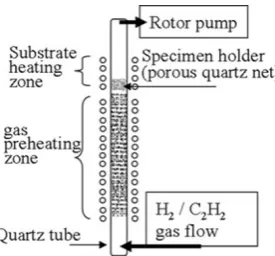
schematic diagram of thermal CVD is shown in Fig.1. In
order to vary the temperature difference between gas and substrate temperatures, the system consists of a gas pre-heating zone and a substrate pre-heating zone. The specimen holder is made of the porous quartz fiber nets for better gas penetration. In other words, the main feature of this system is that the direction of temperature gradient on each cata-lyst can be manipulated. Specimen designations and their deposition conditions are shown in Table 1.
The CNTs Deposition by Plasma-Enhanced CVDs The plasma-enhanced CVDs for CNTs deposition include MP-CVD and ECR-CVD with 2.45 GHz microwave and tunable DC bias. As described in thermal CVD, the Co catalyst for CNTs growth is first deposited on Si wafer by PVD process. The Co-coated substrates are then pre-treated in H-plasma atmosphere to dissociate Co film to become catalyst nanoparticles. The pre-treated substrates are fol-lowed by CNTs deposition with C2H2and H2as reaction
gases (C2H2/H2=10/50 (sccm/sccm)). Specimen
desig-nations and their deposition conditions are listed in Table2.
Characterization Methods
The CNTs on specimens were ultrasonically agitated in acetone to delaminate CNTs from the substrate, disperse and then dry on a copper grid prior to the TEM examina-tion (JEOL JEM-2100F) operated at 200 keV. The TGA (Thermogravimetric Analysis) is used to determine carbon yield as a function of the reaction time under various deposition conditions, where carbon yield is defined by (wt. of carbon, Wc)/(wt. of carbon?catalyst?SBA-15)) for
CNTs deposited on SBA-15 substrate by thermal CVD process.
Results and Discussion
Inherent Condition Differences of Thermal and Plasma-Enhanced CVD
The experiment results revealed that most of the CNTs deposited by plasma-enhanced CVD and by thermal CVD generally grow in the tip-growth [12–21] and base-growth [22–29] modes, respectively. The results indicated the adhesion force between catalyst and substrate to be the main factor in CNT growth modes [11,30]. However, the adhe-sion force mechanism does not fully explain the differences in CNT growth modes in different growth systems. One possible factor that researchers sometimes overlook is the direction of the temperature gradient across the catalyst. In the thermal CVD process, substrate temperatures (TS) are
[image:2.595.101.239.558.686.2]often maintained at a certain level, and reaction gases are generally delivered into the reaction chamber without pre-heating. As a result, the temperature on the top of the cat-alyst (TCt), which is in contact with the flowing gases, is
generally lower than the temperature at the bottom side of
the catalyst (TCb), which is in contact with the substrate
[image:3.595.53.546.72.373.2](Fig.2.) In contrast, with plasma-enhanced CVD, micro-waves generally ionize the reaction gases to attain the plasma state, which often reaches higher temperatures than the substrate temperature. In other words, the temperature at Table 1 Specimen designations and their deposition conditions by thermal CVD
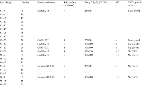
Spec. desig.a tb(min) Catalyst/substrate Sub. surface conditionc
Temp.dTG/TS(°C/°C) DTe CNTs growth
mode
A1–5 5 Co/SBA-15 R 25/800 – Base-growth
A1–10 10
A1–15 15
A1–20 20
A1–30 30
A1–40 40
A1–65 65
A1–90 90
A2–20 20 Co/Si (001) S 25/800 – Base-growth
A3–20 20 Co/SBA-15 R 800/600 ? Tip-growth
A4–20 20 Co/Si (001) S 800/600 ? Tip-growth
A5–20 20 Co/SBA-15 R 650/650 *0 No CNTs
A6–5 5 Co/SBA-15 R 800/800 *0 No CNTs
A6–10 10
A6–15 15
A7–5 5 No cata./SBA-15 R 25/800 – No CNTs
A7–10 10
A7–15 15
A8–5 5 No cata./SBA-15 R 800/800 *0 No CNTs
A8–15 15
A8–25 25
a Other deposition conditions: H
2/C2H2=50/50 (sccm/sccm); 3 kPa pressure b t: CNTs deposition time
c Conditions of the substrate surface,RRough (porous) andSSmooth surface
d T
G: the pre-heated temperature of the reaction gas;TS: the substrate temperature at heating zone
e DT=temperature of catalyst at the top minus at the bottom. Its sign represents the temperature gradient direction
Table 2 Specimen designations and their deposition conditions by plasma-enhanced CVD
Spec. desig. Methoda W
pre/Wgrob (W/W) BiasbVpre/Vgro(V/V) TSbTSi/TSf(°C/°C) Dep. Timec(min) DTd Growth Mode
B1 MP 800/800 100/120 467/500 5 ? Tip-growth
B2 1,000/600 100/60 520/507 2 - Base-growth
C1 ECR 250/270 100/120 500/530 5 ? Tip-growth
C2 300/240 120/100 750/631 4 - Base-growth
a MP Microwave plasma CVD,ECRElectron cyclotron resonance CVD, The working pressures in MP and ECR are 1.3 kPa and 0.9 Pa,
respectively
b W
pre, and Vpre=microwave power, and bias voltage during the H-plasma pre-treatment step (H2=50 sccm), respectively
Wdep, Vdep,TSi, and TSf=microwave power, bias voltage, initial and final substrate temperature of the deposition step (H2/C2H2flow ratio=
50/10 (sccm/sccm); pressure=10 Torr), respectively
c CNTs deposition time in minute
d
[image:3.595.50.545.481.553.2]the top of catalyst particles that are in contact with or are close to the plasma zone is higher than the temperature at the bottom that is in contact with the substrate. Therefore, the direction of the temperature gradient across the catalyst particles is essentially downward and upward in thermal and plasma-enhanced CVD, respectively. These tempera-ture differences are the main reason for differences in CNT growth modes.
By defining DT as the vector quantities of catalyst temperature at the top minus the catalyst temperature at the bottom side [Fig.2and Eq. (1)]DTis generally\0 and[0 for CNTs that come from thermal and plasma-enhanced CVD, respectively. DT is an index for determining the direction of the temperature gradient across the catalyst particles. To examine the effect of DT on CNT growth modes, this study performs experiments designed to vary theDTvalues from negative to positive.
DT ¼TCt=VTCb=S ð1Þ
CNT Growth Under Different Surface Morphologies of Substrate by Thermal CVD
Figure3a, b shows that the typical TEM bright field and corresponding dark field images, respectively, of as-deposited CNTs on nanoporous SBA-15 substrate by thermal CVD without pre-heating reaction gases (Speci-men A1-20). Figures3and4show the corresponding TEM images of CNTs on smooth Si wafers (Specimen A2-20).
These images suggest that CNTs deposited on either nanoporous or smooth substrate surfaces undergo base-growth modes, as the literature reports for CNTs grown by thermal CVD [22–29]. One of the reported factors deter-mining CNT growth modes is the adhesion force between catalyst and substrate [11]. However, it is unlikely to apply in these cases. Since the SBA-15 substrates have a much rougher surface than Si wafer substrates, the adhesion between the catalyst and Si wafer substrates is generally greater than between the catalyst and SBA-15 substrates, due to the decrease in real area in contact [58]. Clearly, the difference in adhesion force between catalysts and sub-strates does not change the CNT growth mode in these cases. In other words, DT\0 may be the main factor in these cases and is also the typical condition in thermal CVD processes.
Fig. 2 Schematic diagrams to show the temperature distribution across a catalyst particle for different deposition systems:athermal CVD andbplasma-enhanced CVD systems
[image:4.595.324.529.55.460.2] [image:4.595.67.274.60.306.2]Effect ofDTon CNT Growth
To further confirm the effect ofDT on CNT growth, this study performed two experiments (Specimens A3-20 and A4-20 in Table1) with the same growth condition of DT[0, designed to deposit CNTs by thermal CVD on the mesoporous SBA-15 and Si wafer substrates, respectively. In these two cases, the reaction gases were pre-heated to higher temperatures than the substrate before entering the reaction chamber to raiseDTover zero. Figures 5a, b and
6a, b show the corresponding TEM images of the tip-growth CNTs deposited on the mesoporous SBA-15 and Si wafer substrates, respectively, under conditions ofDT[0 (Fig.6b is at higher magnification). Except for the catalyst being located at the tip of the CNTs (as the arrows point), the blurred microstructure frequently found in these cases (Figs.5b, 6a) is the most obvious difference compared to
CNTs grown under conditions ofDT\0. One can observe the microstructure of graphite walls and bamboo-like tube structure using a high-resolution TEM (Fig.6b). Figures3,
4 5and 6 suggest that the sign ofDT is the predominant parameter apart from substrate morphology. The effect of adhesion force between the catalyst and substrate does not explain the growth mode of CNTs in these cases.
This study also conducted three experiments (Specimens A6–5, A6–10 and A6–15 in Table1) to deposit CNTs by thermal CVD with the condition ofDT*0. Figure 7a, b shows the typical TEM images of deposits on SBA-15 substrate for Specimen A6–5 (Fig.7b is at higher magni-fication). The SBA-15 images are clear, and the catalysts particles can become poisoned after less than 5 min of deposition time by acquiring graphite-like layers to form an Fig. 4 TEM image of the as-deposited CNTs on Si wafer substrate
by thermal CVD without gas pre-heatinga low magnification and
bhigher magnification images (Specimen A2–20) Fig. 5by thermal CVD with gas pre-heating (gas temperatureTEM images of the as-deposited CNTs on SBA-15 substrate[substrate
[image:5.595.325.529.55.463.2] [image:5.595.70.271.59.447.2]onion-like structure, signifying no obvious growth rate or growth mode.
TGA Curves of CNTs Under VariousDT
TGA analyses of CNTs deposited on SBA-15 substrates by thermal CVD were conducted to determine the wt% of the constituents in the specimen, using a heating rate of 5°C/ minute and air flow rate of 15 sccm. The typical TGA curve from room temperature to 800°C for CNTs deposited by thermal CVD without gas pre-heating is shown in Fig.8
(Specimen A1–20). From the TGA curves, carbon yield, as defined in Eq.2, can be derived, which represents an index of the total carbon content produced after process in the specimen, including CNTs,.
yieldðwt%Þ ¼ Wc
100Ww
100 ð2Þ
where Ww is the first stage weight loss around 100°C,
owing to H2O absorbed in the hydrophilic SBA-15
sub-strate.Wcis the second stage weight loss, attributable to the
oxidation reaction of carbon with oxygen, and the residue weight is mainly attributable to Co/SBA-15 or SBA-15 for specimens without a catalyst.
Figure9shows the curves of carbon yield as a function of deposition time for four different thermal CVD pro-cesses. For conditions of DT\0, Fig.9a, c shows the TGA curves for carbons deposited on SBA-15 substrates under the same substrate and gas temperatures (TS =800°C; TG=25°C) with and without Co catalyst,
respectively (Specimens A1- and A7-series). The slope of Fig. 6 TEM images of the as-deposited CNTs on Si wafer substrate
by thermal CVD with gas pre-heating (gas temperature[substrate temperature):alow magnification andbhigher magnification images (Specimen A4–20)
[image:6.595.325.528.55.451.2] [image:6.595.69.270.57.451.2]the curves is basically the growth rates of various carbon species. In Fig.9a, the curve is roughly dividable into two straight lines, representing the growth of two different species. It is interesting to note that the first and the second straight lines in Fig.9a represent the growth of CNT and non-CNT carbon species, respectively. The following evi-dences confirm this. First, the growth of CNTs can take up to 20 min, as observable in Fig.3, showing the TEM image of CNTs at the intersection of the first and the second lines in Fig.9a. Second, the slope of the second line (0.33 wt%/ min) is almost parallel to that in Fig.9c, which represents the growth of non-CNTs species without catalyst applica-tion. In other words, the catalyst that assists the growth of CNTs becomes poisoned after a certain deposition time (20 min in this case) [21,59–65].
For the condition of DT*0, Fig. 9b, d show two curves of carbon yield as a function of deposition time for growth of CNTs by thermal CVD on SBA-15 substrates with and without Co as catalyst, respectively. Notably, the two curves have almost the same slope. Figure9b and the
TEM onion-like image in Fig.7 suggest that there is no CNTs growth, but rather onion-like carbon growth up to 5 min before Co-catalyst becomes poisoned.
The earlier analyses successfully demonstrate the DT across the catalyst nanoparticle to be one of the major factors in thermal CVD determining the growth mode of CNTs. TheDT is essentially an index of temperature gra-dient direction across a catalyst nanoparticle. The results indicate that the base-growth and tip-growth modes of CNTs by thermal CVD are preferred underDT\0 and[0, respectively.
Growth Mode of CNTs by Plasma-Enhanced CVD To test the effect of DT on the growth mode of CNTs deposited by plasma-enhanced CVD, the MP-CVD and ECR-CVD were used to grow CNTs under DT[0 and DT\0. In the case of plasma-enhanced CVD, the manipulation of DT is obtainable by using the scheme in Fig.10, which shows the temperature variation during the process. During the pre-treatment stage, the temperature is rapidly increased from room temperature to the initial substrate temperature, Tsi, which is defined as the
begin-ning temperature of the substrate during the growth stage of CNTs. Immediately after the substrate’s pre-treatment stage comes a heating or cooling growth stage, which is manipulated by adjusting the microwave power and the substrate bias. The continuous increase or decrease in the substrate temperature signifies heating or cooling from the plasma to the substrate through catalyst nanoparticles, i.e., DT[0 or\0 across the nanoparticle, respectively. The substrate temperatures during the growth stage were
0 200 400 600 800
60 65 70 75 80 85 90 95 100
WC WW
weight loss (wt%)
Temperature (°C)
Fig. 8 TGA curve of the as-deposited CNTs on SBA-15 substrate by thermal CVD without gas pre-heating (Specimen A1–20)
[image:7.595.69.271.59.199.2]Fig. 9 Carbon yield (wt%) versus deposition time curves of the as-deposited CNTs as-deposited by thermal CVD for specimens with different deposition conditions:aA1,bA6,cA7 anddA8-series, respectively
[image:7.595.67.270.247.404.2] [image:7.595.322.525.482.679.2]monitored to insure the heating or cooling effects, and its final temperature,Tsf, appears in Table 2.
Figure11a, b shows TEM images of CNTs deposited by MP-CVD under conditions ofDT[0 and\0, respectively. This indicates that a difference inDTdoes make a differ-ence in the growth mode of CNTs, as the tip-growth and base-growth modes are quite obvious in Fig.11a, b, respectively. Moreover, same conclusions apply for CNTs deposited by ECR-CVD, as Fig.12a, b show in TEM images of CNTs grown under conditions of DT[0 and \0, respectively.
Similar investigation indicates that plasma treatment may also affect the growth mode by decreasing the bond between catalyst and substrate [33]. However, this does little to control or define the bond strength between cata-lysts and substrates, due to the fact that catalyst
nanoparticles are in a liquid state during the high temper-ature CNT growth process [5, 66]. In other words, our experimental results suggest an alternative synthesis route to achieve CNTs with a customized growth mode, which can probably overcome the uncertainty of adhesion force. Controlling the temperature gradient direction can achieve both modes of CNTs by thermal CVD, MP-CVD and ECR-CVD.
ProposedDTModel for CNT Growth Modes
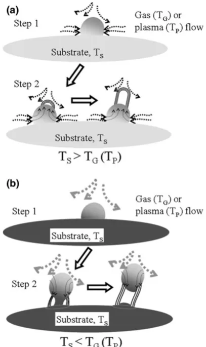
[image:8.595.325.526.268.665.2]Figure13a, b illustrates the conditions ofDT\0 and[0, respectively, elucidating the effect of DTon CNT growth modes. The process during growth stage is roughly divid-able into two steps. Figure13a illustrates the concept of the
Fig. 11 TEM images of the as-deposited CNTs on Si wafer substrate by MP-CVD with schemes ofatemperature-rising andb temperature-declining sequences in Fig.10, respectively (Specimens B1 and B2)
[image:8.595.70.271.270.675.2]base-growth mode (DT\0), which is the mode of tradi-tional thermal CVD systems and specially designed plasma-enhanced CVD systems. In Step 1, the precursors are decomposed and/or reacted with the substrate to pro-duce carbon species; they are then dissolved by catalyst nanoparticles. The solution of carbon species in the catalyst nanoparticle can proceed until reaching the solubility limit at the substrate temperature. In Step 2, the cooling effect of precursor flow causes the temperature at the top surface of the catalyst particle to be lower than the temperature at the bottom surface. Therefore, carbon supersaturation in the catalyst is higher close to its top surface than to its bottom surface. Carbon precipitation is thus more likely to occur on the top surface of the catalyst to form base-growth CNTs. Furthermore, due to its endothermic nature, the precipitation of carbon on the top surface of catalysts can result in a local cooling effect and can further enhance the DT effect [62, 67]. In contrast, Fig.13b illustrates the condition ofDT[0, where the gas or plasma is at a higher temperature than the substrate. In this case, carbon in the catalyst is likely to precipitate on the cooler bottom side, pushing the catalyst upward to form tip-growth CNTs.
Conclusions
This study’s experiments successfully demonstrate the effect of DT on CNT catalyst nanoparticles deposited on SBA-15 and Si wafer substrates by thermal and plasma-enhanced CVD. This study definesDTas the temperature at the top surface side minus the temperature at the bottom side of a catalyst particle during a CNT’s growth stage. It is essentially an index of the temperature gradient direction across a catalyst particle. This study’s results demonstrate that tip-growth and base-growth CNTs have a greater tendency to form under the conditions of DT[0 and\0, respectively. When DT=0, the non-CNTs or onion-like carbon may be more likely to form. This study proposes mechanisms to explain effect ofDTon CNT growth modes. Acknowledgments The authors would like to acknowledge the support of the National Science Council of Taiwan, under Contract No. NSC 98-2221-E-451-001.
Open Access This article is distributed under the terms of the Creative Commons Attribution Noncommercial License which per-mits any noncommercial use, distribution, and reproduction in any medium, provided the original author(s) and source are credited.
References
1. S. Iijima, Nature354, 56 (1991)
2. J. Wei, B. Jiang, X. Zhang, H. Zhu, D. Wu, Chem. Phys. Lett. 376, 753 (2003)
3. S. Iijima, T. Ichihashi, Nature363, 603 (1993)
4. D.S. Bethune, C.H. Klang, M.S. de Vries, G. Gorman, R. Savoy, J. Vazquez, R. Beyers, Nature363, 605 (1993)
5. R. Saito, M. Fujita, G. Dresselhaus, M.S. Dresselhaus, Appl. Phys. Lett.60, 2204 (1992)
6. H. Zhu, K. Suenaga, A. Hashimoto, K. Urita, S. Iijima, Small1, 1180 (2005)
7. M. Ge, K. Sattler, Appl. Phys. Lett.65, 18–2284 (1994) 8. S. Amelinckx, X.B. Zhang, D. Bernaerts, X.F. Zhang, V. Ivanov,
J.B. Nagy, Science265, 635 (1994)
9. D. Bernaerts, X.B. Zhang, X.F. Zhang, S. Amelinckx, G. Van Tendeloo, J. Van Landuyt, V. Ivanov, J.B. Nagy, Philos. Mag. A 71, 605 (1995)
10. Z.W. Pan, S.S. Xie, B.H. Chang, L.F. Sun, W.Y. Zhou, G. Wang, Chem. Phys. Lett.299, 97 (1999)
11. C. Bower, O. Zhou, W. Zhu, D.J. Werder, S. Jin, Appl. Phys. Lett.77, 2767 (2000)
12. A.J. Hart, B.O. Boskovic, A.T.H. Chuang, V.B. Golovko, J. Robertson, B.F.G. Johnson, A.H. Slocum, Nanotechnology17, 1397 (2006)
13. C.T. Kuo, C.H. Lin, A.Y. Lo, Diam. Relat. Mater.12, 799 (2003) 14. C.H. Lin, H.L. Chang, C.M. Hsu, A.Y. Lo, C.T. Kuo, Diam.
Relat. Mater.12, 1851 (2003)
15. Y. Abdi, J. Koohsorkhi, J. Derakhshandeh, S. Mohajerzadeh, H. Hoseinzadegan, M.D. Robertson, J.C. Bennet, X. Wu, H. Radamson, Mater. Sci. Eng. C26, 1219 (2006)
16. H.Y. Yap, B. Ramaker, A.V. Sumant, R.W. Carpick, Diam. Relat. Mater.15, 1622 (2006)
[image:9.595.68.272.57.400.2]17. Z.F. Ren, Z.P. Huang, J.W. Xu, J.H. Wang, P. Bush, M.P. Siegal, P.N. Provencio, Science282, 1105 (1998)
18. C.M. Hsu, C.H. Lin, H.L. Chang, C.T. Kuo, Thin Solid Films 420, 225 (2002)
19. H. Murakami, M. Hirakawa, C. Tanaka, H. Yamakawa, Appl. Phys. Lett.76, 1776 (2000)
20. Y. Chen, D.T. Shaw, L. Guo, Appl. Phys. Lett. 76, 2469 (2000)
21. P.L. Chen, J.K. Chang, C.K. Kuo, F.M. Pan, Diam. Relat. Mater. 13, 1949 (2004)
22. C.J. Lee, J. Park, Appl. Phys. Lett.77, 3397 (2000)
23. S. Fan, M.G. Chapline, N.R. Franklin, T.W. Tombler, A.M. Cassell, H. Dai, Science283, 512 (1999)
24. G.S. Choi, Y.S. Cho, S.Y. Hong, J.B. Park, K.H. Son, D.J. Kim, J. Appl. Phys.91, 3847 (2002)
25. G. Gulino, R. Vieira, J. Amadou, P. Nguyen, M.J. Ledoux, S. Galvagno, G. Centi, C. Pham-Huu, Appl Catal A Gen 279, 89 (2005)
26. N. Zhao, C. He, Z. Jiang, J. Li, Y. Li, Mater. Lett.60, 159 (2006) 27. C.J. Lee, S.C. Lyu, Y.R. Cho, J.H. Lee, K.I. Cho, Chem. Phys.
Lett.341, 245 (2001)
28. K.S. Choi, Y.S. Cho, S.Y. Hong, J.B. Park, D.J. Kim, J. Eur. Ceram. Soc.21, 2095 (2001)
29. C.J. Lee, D.W. Kim, T.J. Lee, Y.C. Choi, Y.S. Park, Y.H. Lee, W.B. Choi, N.S. Lee, G.S. Park, J.M. Kim, Chem. Phys. Lett. 312, 461 (1999)
30. A.C. Dupuis, Prog. Mater. Sci.50, 929 (2005)
31. A.V. Melechko, V.I. Merkulov, D.H. Lowndes, M.A. Guillorn, M.L. Simpson, Chem. Phys. Lett.356, 527 (2002)
32. W.Y. Lee, T.X. Liao, Z.Y. Juang, C.H. Tsai, Diam. Relat. Mater. 13, 1232 (2004)
33. A. Malesevic, H. Chen, T. Hauffman, A. Vanhulsel, H. Terryn, C.V. Haesendonck, Nanotechnology18, 455602 (2007) 34. C. Li, H. Zhu, K. Suenaga, J. Wei, K. Wang, D. Wu, Mater. Lett.
63, 1366 (2009)
35. K. Hernadi, L. Thin-Nga, L. Forr, J. Phys. Chem. B105(50), 12464 (2001)
36. K. Akagi, R. Tamura, M. Tsukasa, Phys. Rev. Lett. 74, 2307 (1995)
37. X. Chen, S. Motojima, H. Iwanaga, Carbon37, 1825 (1999) 38. J. Cheng, X. Zhang, J. Tu, X. Tao, Y. Ye, F. Liu, Mater. Chem.
Phys.95, 12 (2006)
39. W.H. Wang, K.M. Chao, C.T. Kuo, Diam. Relat. Mater.14, 753 (2005)
40. R. Moradian, A. Fathalian, Nanotechnology17, 1835 (2006) 41. G. Wu, B.Q. Xu, J. Power Sources174, 148 (2007)
42. H.L. Chang, C.H. Lin, C.T. Kuo, Thin Solid Films420–421, 219 (2002)
43. S.S. Wong, J.D. Harper, P.T. Lansbury Jr., C.M. Lieber, J. Am. Chem. Soc.120, 603 (1998)
44. C.V. Nguyen, K.J. Chao, R.M. Stevens, L. Delzeit, A. Cassell, J. Han, M. Meyyappan, Nanotechnology12, 363 (2001) 45. F. Ding, A.R. Harutyunyan, B.I. Yakobson, PNAS 106, 2506
(2009)
46. S. Reich, L. Li, J. Robertson, Chem. Phys. Lett.421, 469 (2006) 47. R. Gao, Z.L. Wang, S. Fan, J. Phys. Chem. B104(6), 1227 (2000) 48. F. Ding, A. Rose, K. Bolton, Carbon43, 2215 (2005)
49. W.H. Wang, Y.R. Peng, P.K. Chuang, C.T. Kuo, Diam. Relat. Mater.15, 1047 (2006)
50. H. Kanzow, A. Ding, Phys. Rev. B60, 11–180 (1999)
51. C.M. Hsu, H.J. Lai, C.T. Kuo, J. Vac. Sci. Technol. A22, 1461 (2004)
52. R.A. Segura, W. Iba´n˜ez, R. Aoto, S. Hevia, P. Ha¨berle, J. Nanosci. Nanotechnol.6, 1945 (2006)
53. I.K. Song, W.J. Yu, Y.S. Cho, G.S. Choi, D. Kim, Nanotech-nology15, S590 (2004)
54. C.C. Lin, P.Y. Lo, C.H. Lin, C.T. Kuo, Diam. Relat. Mater.14, 778 (2005)
55. A. Gohier, C.P. Ewels, T.M. Minea, M.A. Djouadi, Carbon46, 1331 (2008)
56. M. Chhowalla, K.B.K. Teo, C. Ducati, N.L. Rupesinghe, G.A.J. Amaratunga, A.C. Ferrari, D. Roy, J. Robertson, W.I. Milne, J. Appl. Phys.90, 5308 (2001)
57. D. Zhao, J. Feng, Q. Huo, N. Melosh, G.H. Fredrickson, B.F. Chmelka, G.D. Stucky, Science279, 548 (1998)
58. Y.I. Rabinovich, J.J. Adler, A. Ata, R.K. Singh, B.M. Moudgil, J. Colloid Interface Sci.232, 10 (2000)
59. S.K. Pal, S. Talapatra, S. Kar, L. Ci, R. Vajtai, T. Borca-Tasciuc, L.S. Schadler, P.M. Ajayan, Nanotechnology19, 1 (2008) 60. K.Y. Lee, S.I. Honda, M. Katayama, T. Miyake, K. Himuro,
K. Oura, J.G. Lee, H. Mori, T. Hirao, J. Vac. Sci. Technol. B 23(4), 1450 (2004)
61. D.N. Futuba, K. Hata, T. Yamada, K. Mizuno, M. Yumura, S. Iijima, Phys. Rev. Lett.95, 056104-1 (2005)
62. H. Kanzow, A. Schmalz, A. Ding, Chem. Phys. Lett.295, 525 (1998)
63. G.S. Duesberg, A.P. Graham, F. Kreupl, M. Liebau, R. Seidel, E. Unger, W. Hoenlein, Diam. Relat. Mater.13, 354 (2004) 64. M. Stadermann, S.P. Sherlock, J.B. In, F. Fornasiero, H.G. Park,
A.B. Artyukhin, Y. Wang, J.J.D. Yoreo, C.P. Grigoropoulos, O. Bakajin, A.A. Chernov, A. Noy, Nano lett.9, 738 (2009) 65. H.J. Jeong, Y.M. Shin, S.Y. Jeong, Y.C. Choi, Y.S. Park,
S.C. Lim, G.S. Park, I.T. Han, J.M. Kim, Y.H. Lee, Chem. Vap. Deposition8, 11 (2002)
66. Y. Homma, Y. Kobayashi, T. Ogino, D. Takagi, R. Ito, Y.J. Jung, P.M. Ajayan, J. Phys. Chem. B107, 12161 (2003)