N A N O E X P R E S S
Open Access
Broadband Perfect Absorber with
Monolayer MoS
2
and Hexagonal Titanium
Nitride Nano-disk Array
Dewang Huo
1, Jingwen Zhang
1,2, Hao Wang
1, Xiaoxuan Ren
1, Chao Wang
1, Hang Su
1and Hua Zhao
1,2*Abstract
A broadband metamaterial absorber (MA) composed of hexagonal-arranged single-sized titanium nitride (TiN) nano-disk array and monolayer molybdenum disulfide (MoS2) is studied using finite-difference time-domain (FDTD) simulations. The structure of TiN nano-disk array/dielectric silica (SiO2)/aluminum (Al) is adopted in our design. By optimizing the dimension parameters of the structure, an average absorption of 96.1% is achieved from 400 to 850 nm. In addition, by inserting a monolayer MoS2which has high absorption at the short wavelength side underneath the TiN nano-disk array, an average absorption of 98.1% over the entire visible regime from 400 to 850 nm was achieved, with a peak absorption near 100% and absorption over 99% from 475 to 772 nm. Moreover, the absorber presented in this paper is polarization insensitive. This compact and unique design with TiN nano-disk/ monolayer MoS2/ SiO2/Al structure may have great potential for applications in photovoltaics and light trapping.
Keywords:Metamaterial absorber, Finite difference time domain, Titanium nitride, Hexagonal nano-disk array, Monolayer MoS2
Background
Metamaterials are able to tailor the amplitude, phase, and polarization responses of the incident light in an un-precedented way. In particular, absorption enhancement with metamaterials is one of the most interesting topics associated artificially engineered metamaterials [1–5]. Several metamaterial structures were demonstrated as high-performance light absorbers, such as dense nano-rods and nanotubes [6, 7], multilayer planar photonic structures [8–10], and photonic crystals [11]. In the past decade, Au [12] and Ag have been intensively investigated [13–16] for designing absorbers. At earlier stage, most research activities have focused on the absorption of the electromagnetic field within a narrow waveband with structures of metal nanoparticles, periodic gratings, and metal/dielectric/metal thin layers [17–20]. However, broadband absorption throughout the entire visible regime is important for photovoltaic and thermo-photovoltaic
cells. Driven by real needs in realistic applications, re-search works on broadband absorption were reported in recent years. The absorber with a nanostructured top sil-ver film composed of crossed trapezoidal arrays offers broadband and polarization-independent resonant light absorption with an average measured absorption of 0.71 against a simulated absorption of 0.85 over the entire vis-ible regime (400–700 nm) [16]. The broadband absorption was further improved with an absorber based on multiple metal/dielectric/ metal layers with an average simulated absorption of 93% over the entire visible region [14]. In order to get better broadband absorption, semiconductor-based oxides and transition metal nitrides [21, 22] were proposed as alternative plasmonic materials. Specifically, transition-metal nitrides such as TiN or ZrN can serve as substitutes for conventional noble metals in the visible waveband [21]. A broadband metamaterial absorber based on TiN with square ring array shows an average absorp-tion of 95% over the entire visible regime (400–800 nm) [23]. And absorption over 98% from 560 to 675 nm was obtained in a broadband metamaterial absorber with TiN and indium tin oxide transparent conducting films, while
* Correspondence:[email protected]
1Institute of Modern Optics, Department of Physics, Harbin Institute of Technology, Harbin 150001, China
2Key Laboratory of Micro-Optics and Photonics Technology of Heilongjiang Province, Harbin 150001, China
the average absorption was less than 85% for the short waves from 400 nm to 500 nm [24]. Recently, monolayer MoS2 shows great potential for generating various
opto-electronic devices [25–34] and for photocatalytic applica-tions owing to high absorption at the short wavelength side [35, 36]. The broadband absorber with metal Ag metasurface and a monolayer MoS2was studied yet with
average absorption less than 90% [37]. In this work, a more compact absorber with a monolayer MoS2 and
hexagonal-arranged TiN nano-disk array is proposed, with as high as 98.1% average absorption over the entire visible region extending to near-IR (from 400 to 850 nm). This structure should be promising for photovoltaic applications.
Methods
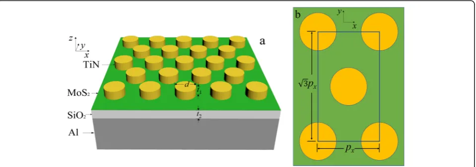
The initial structure of our absorber and the top view of a unit cell are schematically shown in Fig. 1. A layer of dielectric SiO2 is sandwiched between a TiN nano-disk
array and an aluminum (Al) substrate. The single-sized TiN nano-disks are hexagonally arrayed upon the SiO2
film with the same pitch. A monolayer MoS2of
thick-ness 0.625 nm is inserted underneath the nano-disk array. The structure parameters are denoted as follows:
px andpy= pffiffiffi3px are the periodic lengths of the rect-angle unit cell along the x- and y-directions, respect-ively;d is the diameter of the TiN nano-disk;t1andt2
are the thicknesses of the top TiN nano-disk and the SiO2film, respectively. An aluminum film is chosen as
the substrate with thickness 500 nm, far thicker than the light penetration depth in the spectral range we studied.
The finite-difference time-domain (FDTD) method was employed in the simulation with the software package from Lumerical FDTD Solutions. The light is assumed in-cident normally on the absorber towards the−z-direction.
In this simulation, the z-direction has two perfectly matched layers, and the periodic boundary conditions are set in thex- andy-directions. The absorbance can be cal-culated from the corresponding transmittance (R) and transmittance (T) withA= 1−R−T. It is easy to see the transmittance is always zero in our case because the Al substrate is far thicker than the light penetration depth in the spectral range and serves as a mirror in forming a resonance cavity with the nano-disk array to enhance the absorption. In the simulations, non-uniform mesh sizes were used in regard to different layer sizes and the specific settings were as following: a mesh size of 2.0 nm × 2.0 nm × 0.1 nm was employed in the monolayer MoS2; a mesh size of 2.0 nm × 2.0 nm × 2.0 nm was set in
other simulating regions.
The refractive index curve of SiO2 spacer layer was
adopted from the material base of the software Lumeri-cal FDTD Solutions. The related material parameters of TiN were borrowed from Ref. [38], and the dispersion curve of the monolayer MoS2 was obtained from Ref.
[39]. The fitted dispersion curves of TiN and monolayer MoS2 are exhibited in Fig. 2. In the visible regime, the
TiN is proposed to replace the noble metal like Au or Ag in realizing the excitation of LSPR [21], since the TiN shows much higher extinction coefficient compared to the noble metals. However, relatively low extinction coefficient at the shortwave edge indicates unsatisfying absorption performance. Fortunately, a monolayer MoS2
possesses quite high extinction coefficients, especially at the short wave side; it can be introduced to the TiN nano-disk/SiO2/Al structure to improve broadband
ab-sorption over the entire visible regime. In addition, the monolayer MoS2is of direct-gap semiconductor in which
the electrons can be easily excited. And with decent thermoelectric property [40], it would make good use of the energy absorbed by the proposed structure and benefit for the solar energy applications.
[image:2.595.60.540.545.714.2]Results and Discussion
The absorption performance of the TiN nano-disk/SiO2/
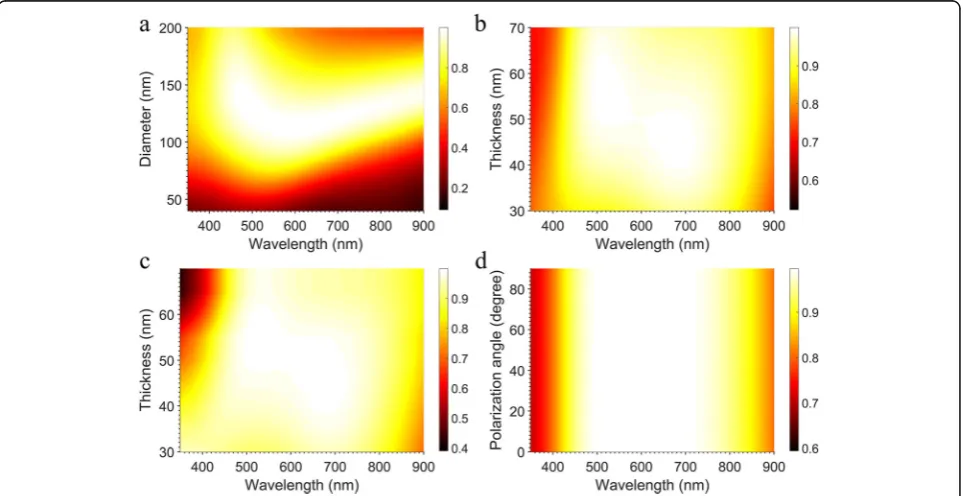
Al structure is studied firstly. In order to optimize the performance of the structure, the dependences of the ab-sorption spectra on the diameter and the thickness of TiN nano-disks, and the thickness of SiO2 spacer layer,
respectively, have been studied with x-polarized incident light with the optimized periodpxat 200 nm.
Since the electric and magnetic fields in the unit cells are strongly influenced by the dimensions of the ab-sorber [28, 41], the absorption spectra with the different diameters of TiN nano-disks were studied. Figure 3a shows the absorption spectra versus diameters of the top TiN nano-disks for px = 200 nm, and t1 =t2= 50 nm.
The resonance absorption increases when the diameter
of the TiN nano-disks increases from 40 to 120 nm, then the absorption decreases with the diameter gradually ap-proaching to 200 nm. Structure proposed possesses the best absorption performance over the visible regime when the diameter is around 120 nm.
For the same reason, the absorption dependence on the thicknesses of TiN nano-disks was also investigated. Figure 3b shows the absorption spectra versus the thick-ness of the top TiN nano-disks when other parameters were fixed atpx= 200 nm,d= 120 nm, andt2= 50 nm.
It is apparent that the resonance absorption peak wavelength has a redshift while the t1 increases, and
the resonance absorption bandwidth becomes wider from
t1= 30 to 50 nm. As a result, for t1= 50 nm, the best
absorption performance is achieved with wavelengths
Fig. 2aDispersion of TiN layer:nis the refractive index andkextinction coefficient.bDispersion of monolayer MoS2
Fig.3aAbsorption spectra versus diameter of the top TiN nano-disk with the parameters fixed atpx= 200 nm, andt1=t2= 50 nm.bAbsorption
spectra versus thickness of the top TiN nano-disks withpx= 200 nm,d= 120 nm, andt2= 50 nm.cAbsorption spectra versus thickness of the
[image:3.595.58.539.88.211.2] [image:3.595.58.540.436.684.2]ranging from 453 to 797 nm, which is about 350 nm wide, with the absorption higher than 95%.
Moreover, the thickness of the SiO2spacer layer is also
a crucial parameter for determining magnetic resonance of the structure. From the absorption spectra versus thickness of SiO2 spacer layer in Fig. 3c, it is seen that
the central wavelength of the resonance absorption peak is redshifted with increasing thickness of SiO2, and the
optimized thickness ist2= 50 nm while the rest
parame-ters were set atpx = 200 nm, d = 120 nm, t1= 50 nm.
One can see that the TiN nano-disk/SiO2/Al structure
offers a quite satisfying broadband absorption with an average absorption of 96.1% from 400 to 850 nm.
To understand the mechanism behind the absorption peak around 680 nm in Fig. 4a, the coupled dipole ap-proximation approach was employed by treating a nano-disk as a polarizable dipole. Since the size of a TiN nano-disk is far smaller than the wavelength of visible light, the quasi-static approximation is valid in dealing with the case. In the quasi-static approximation, each nano-disk illuminated with incident light could be treated as a dipole with polarizability [42],
α∝V ε1−ε2
ε2þLðε1−ε2Þ ð
1Þ
Here,Vdenotes the volume of TiN disk,ε1=ε1r+ε1iis
the frequency-dependent dielectric permittivity of TiN nano-disk, andε2is the dielectric constant of embedding
medium SiO2. When the applied electric field of the
in-cident light is polarized parallel to the disk (i.e., xy
plane), the shape factor can be written as [42]
L¼ g 2e2
π 2−tan
−1g
−g2
2 ð2Þ
g¼
ffiffiffiffiffiffiffiffiffiffi
1−e2
e2
r
ð3Þ
e2¼1−4t
2 1
d2 ð4Þ
Here, dis the diameter of the TiN nano-disk andt1is
the thickness of the TiN nano-disk. Thus, the optical ex-tinction cross section σextcan be obtained from the
po-larizability [12, 43]
σext∝kImð Þα ð5Þ
As aforementioned, the quasi-static approximation is applicable in calculating the optical extinction cross sec-tion of a single TiN nano-disk. The normalized optical extinction cross section of the nano-disk is shown in Fig. 4b, which has similar trend to the spectrum in Fig.4a with px = 200 nm,d = 120 nm,t1= 50 nm, and
t2 = 50 nm. The corresponding wavelength for the
maximum optical extinction cross section is about 715 nm, close to the peak wavelength around 680 nm of the absorption spectrum from the simulation result. Indeed, the numerical result is not completely consistent with the absorption spectrum, because we only took the dimensions of TiN nano-disk into consideration to simu-late the LSPR absorption peak but ignored the cross talks between the nano-disks and the magnetic resonance in the gap which should have significant influence on broad-ening the perfect absorption band and contribute to the improvement of the absorption performance in our struc-ture. This will be explained in the following sections.
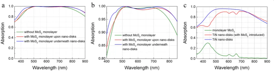
To raise absorption at the short wavelength edge, a monolayer MoS2is introduced into the TiN nano-disk/
SiO2/Al structure as shown in Fig. 1a, by inserting it
upon and underneath the nano-disk array, respectively. The parameters were set as px = 200 nm, d = 120 nm,
t1= 50 nm, andt2= 50 nm based on optimized results
obtained previously. The electric field around the nano-disks is enhanced due to the excitation of LSPR as shown in Fig. 6. Consequently, the enhanced electric field strengthens the absorption in ultrathin monolayer
Fig. 4aAbsorption spectra without monolayer MoS2forpx= 200 nm,d= 120 nm, andt1=t2= 50 nm.bNormalized optical extinction cross
[image:4.595.54.540.493.706.2]MoS2, resulting in better absorption performance for the
both cases as shown in Fig. 5a, b. Without MoS2in the
TiN nano-disk/SiO2/Al structure, the best absorption
performance is obtained with a peak absorption near 100% and average absorption of 96.1% from 400 to 850 nm. With the monolayer MoS2inserted underneath
the TiN nano-disk array, a peak absorption near 100% is also observed. Compared to the case without monolayer MoS2, the band of absorption over 95% is broadened
about 80 nm ranging from 424 to 842 nm, and the ab-sorption of light wavelength at 400 nm is increased from 81 to 89%. As a result, the average absorption from 400 to 850 nm is improved from 96.1 to 98.1% with an about 300-nm wide wavelength range for the near 100% absorp-tion from 475 to 772 nm. With MoS2 layer upon the
nano-disk array, the total performance is also improved with averaged absorption of 96.8% from 400 to 850 nm. From the discussion above, it is seen that inserting mono-layer MoS2underneath the nano-disk array performs
bet-ter in improving the absorption performance the structure proposed. To clarify the contribution of the monolayer MoS2to the total structure, the absorptions of monolayer
MoS2and TiN nano-disks were calculated and shown in
Fig. 5c. After introducing a monolayer MoS2, the
absorp-tion of the nano-disks at short wavelength edge slightly decreases. However, due to high absorption in monolayer MoS2, the total absorption is still increased at short
wave-length edge of the spectra. At the long wavewave-length edge, the absorption by the nano-disks gets higher with introdu-cing monolayer MoS2. As a whole, the absorption
band-width is widened with the monolayer MoS2 underneath
the TiN nano-disks.
Furthermore, the influence of polarization angle of incident light has also been studied. Figure 3d shows that the absorption spectra are barely influenced by the polarization angle of the incident light, as reported in some other metamaterial design [44–46]. The rotational symmetry of circular nano-disk ensures no difference with varying polarization angle at normal incidence. Additionally, the hexagonal array has a threefold rotational
symmetry which makes the absorption insensitive to the polarization angle at normal incidence [44–47]. As a re-sult, the total absorption in the structure is polarization insensitive.
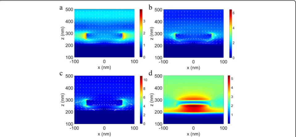
To see how light is absorbed in MA structure, the field distributions and Poynting vectors which represent the energy flows for different resonant wavelengths are studied. In Fig. 6a–c, the electric field distributions are plotted on a cross section through the xz plane at
y = 0, which indicate that the LSPR occurs to enhance the electromagnetic field around the nano-disk and confined the electromagnetic field among nano-disks in all the three cases corresponding to wavelengths 402, 502, and 680 nm, respectively. The parameters were set as px = 200 nm, d = 120 nm, t1 = 50 nm, and
t2 = 50 nm. Comparing the three cases, the LSPR at
402 nm is relatively weak and the reflection electric field is strong, indicating a weak absorption of 82%. For the 502 and 680-nm wavelengths, the LSPRs are obvi-ously stronger (shown in Fig. 6b, c), resulting in better absorptions of 99.4 and 99.6%, respectively. For a better understanding, the Poynting vectors are also plotted with electric field distributions. The greater magnitude of Poynting vector can be seen in the vicinity of nano-disk, especially for the cases with wavelengths of 502 and 680 nm. From the pattern of Poynting vector, a conclusion can be drawn that strong resonance around the nano-disk occurs and the energy flows into the nano-disk, i.e., the in-cident light energy is mainly absorbed by TiN nano-disks. Moreover, the enhanced field around the TiN nano-disks resulting from the LSPR improves the absorption in monolayer MoS2which broadens the absorption band of
TiN nano-disk/SiO2/Al structure for both the cases of
monolayer MoS2inserted upon and underneath the
nano-disk array.
To delve deeper, Figure 7a–c show field intensity dis-tributions on the top surface of nano-disks (interface 1), the interface between the TiN nano-disks and SiO2layer
(interface 2), and the interface between the SiO2 layer
and bottom Al substrate (interface 3) of a unit cell along
Fig. 5The absorption spectraaand the enlarged absorption spectrabof the cases that the monolayer MoS2is introduced underneath TiN
[image:5.595.63.538.581.704.2]the xy plane at the resonance wavelength 680 nm, re-spectively. All the intensity distributions are symmetric, and the maximum resonance intensity is at the edges of the TiN nano-disks indicating that oscillating charges ac-cumulate there (Fig. 7a–c). Regarding interface 3, the resonance intensity is attenuated compared to that of interface 2 due to the scattering electromagnetic field by the nano-disks traveling through the SiO2 spacer layer
along different directions. As Fig. 6d shows, the mag-netic resonance is excited in the gap, which results in an artificial magnetic moment that interacts strongly with the magnetic field of the incident light [48]. Therefore, the electromagnetic field can be enhanced in the gap, and the energy is efficiently confined to the gap between TiN nano-disks and the Al substrate. When the LSPR and magnetic resonance are impedance-matched, the
total absorption arrives at unity [19]. With increasing nano-disk diameter, the cross talks become stronger, leading to changing impedance-matching condition. As a result, one absorption peak splits into two absorption peaks at wavelengths 502 nm and 680 nm, where the LSPR and magnetic resonance are impedance-matched to unity absorption. In addition, the existence of mag-netic resonance makes the monolayer MoS2 inserted
underneath nano-disk array perform better than upon the nano-disk array. Above all, the broadband perfect absorption is obtained owing to excitation of the strong LSPR of nano-disks and magnetic resonance in the gap, along with the cross talks between the adjacent nano-disks. With the developed nanofabrication technology, our design can be realized by the process of thin film de-position and etching.
Fig. 6The distributions of the electric field|E|and the Poynting vectors in thexzplane aty= 0 of a unit cell illuminated with light at wavelengthsλ= 402 nm (a), 502 nm (b), and 680 nm (c), as well as the magnetic field distribution
[image:6.595.59.539.88.310.2] [image:6.595.58.542.568.703.2]Conclusion
In this work, a metamaterial perfect absorber in the waveband from 400 nm to 850 nm has been studied by the FDTD method. Our initially proposed TiN nano-disks/monolayer MoS2/SiO2/Al structure offers a
broad-band perfect absorption of average 98.1% from 400 nm to 850 nm, including an 300-nm bandwidth with near 100% (over 99%) absorption from 475 nm to 772 nm. The realization of the intriguing absorption is on ac-count of the strong LSPR, cross talks of TiN nano-disks, and the magnetic resonance in the gap. Importantly, introducing a monolayer MoS2 have improved
signifi-cantly the absorption performance. In addition, the perfect absorber shows polarization-insensitivity at normal inci-dence. In terms of compactness, the dimension of the metamaterial absorber can be reduced to 150 nm thick. In conclusion, the perfect absorber proposed in this work with the hexagonally periodic, circularly shaped TiN nano-disk pattern and monolayer MoS2offers broadband
near unity absorption and is promising for photovoltaic devices and light trapping.
Abbreviations
FDTD:Finite-difference time-domain; LSPR: Localized surface plasmon resonance; MA: Metamaterial absorber
Funding
This work is supported by Natural National Science Foundation of China (NSFC) (11374076).
Authors’Contributions
DH and HW were mainly responsible for the design and calculation. The main work of XR, CW, and HS were contributed to the design with valuable advices. JZ and HZ helped to draft the manuscript. All authors read and approved the final manuscript.
Ethics Approval and Consent to Participate Not applicable.
Consent for Publication Not applicable.
Competing Interests
The authors declare that they have no competing interests.
Publisher’s Note
Springer Nature remains neutral with regard to jurisdictional claims in published maps and institutional affiliations.
Received: 24 May 2017 Accepted: 15 July 2017
References
1. Chen H, O'Hara JF, Azad AK, Taylor AJ (2011) Manipulation of terahertz radiation using metamaterials. Laser Photonics Rev 5(4):513–533 2. Watts CM, Liu X, Padilla WJ (2012) Metamaterial electromagnetic wave
absorbers. Adv Mater 24 (23):OP98-120
3. Pu M, Feng Q, Hu C, Luo X (2012) Perfect absorption of light by coherently induced plasmon hybridization in ultrathin metamaterial film. Plasmonics 7(4):733–738
4. Isenstadt A, Xu J (2013) Subwavelength metal optics and antireflection. Electron Mater Lett 9(2):125–132
5. Akimov YA, Ostrikov K, Li E (2009) Surface plasmon enhancement of optical absorption in thin-film silicon solar cells. Plasmonics 4(2):107–113
6. Lenert A, Bierman DM, Nam Y, Chan WR, CelanovićI, SoljačićM, Wang EN (2014) A nanophotonic solar thermophotovoltaic device. Nat Nanotechnol 9(2):126–130
7. Xi J, Schubert MF, Kim JK, Schubert EF, Chen M, Lin S, Liu W, Smart JA (2007) Optical thin-film materials with low refractive index for broadband elimination of Fresnel reflection. Nat Photonics 1(3):176–179
8. Shimizu M, Kohiyama A, Yugami H (2015) High-efficiency solar-thermophotovoltaic system equipped with a monolithic planar selective absorber/emitter. J Photonics Energy 5(1):053099–053099
9. Deng H, Li Z, Stan L, Rosenmann D, Czaplewski D, Gao J, Yang X (2015) Broadband perfect absorber based on one ultrathin layer of refractory metal. Opt Lett 40(11):2592–2595
10. Raman AP, Anoma MA, Zhu L, Rephaeli E, Fan S (2014) Passive radiative cooling below ambient air temperature under direct sunlight. Nature 515(7528):540–544
11. Chou JB, Yeng YX, Lee YE, Lenert A, Rinnerbauer V, Celanovic I, SoljačićM, Fang NX, Wang EN, Kim S-G (2014) Enabling ideal selective solar absorption with 2D metallic dielectric photonic crystals. Adv Mater 26(47):8041–8045 12. Bohren CF, Huffman DR (2008) Absorption and scattering of light by small
particles. John Wiley & Sons, New York
13. Wang W, Wu S, Reinhardt K, Lu Y, Chen S (2010) Broadband light absorption enhancement in thin-film silicon solar cells. Nano Lett 10(6):2012–2018 14. Ko H, Ko D, Cho Y, Han IK (2014) Broadband light absorption using a
multilayered gap surface plasmon resonator. Appl Phys A Mater Sci Process 116(3):857–861
15. Cao T, Wei C, Simpson RE, Zhang L, Cryan MJ (2014) Broadband polarization-independent perfect absorber using a phase-change metamaterial at visible frequencies. Sci Rep 4:3955
16. Aydin K, Ferry VE, Briggs RM, Atwater HA (2011) Broadband polarization-independent resonant light absorption using ultrathin plasmonic super absorbers. Nat Commun 2:517
17. Cesario J, Quidant R, Badenes G, Enoch S (2005) Electromagnetic coupling between a metal nanoparticle grating and a metallic surface. Opt Lett 30(24):3404–3406
18. Kachan S, Stenzel O, Ponyavina A (2006) High-absorbing gradient multilayer coatings with silver nanoparticles. Appl Phys B Lasers Opt 84(1):281–287 19. Landy NI, Sajuyigbe S, Mock JJ, Smith DR, Padilla WJ (2008) Perfect
metamaterial absorber. Phys Rev Lett 100(20):207402
20. Hao J, Wang J, Liu X, Padilla WJ, Zhou L, Qiu M (2010) High performance optical absorber based on a plasmonic metamaterial. Appl Phys Lett 96(25):251104
21. Naik GV, Kim J, Boltasseva A (2011) Oxides and nitrides as alternative plasmonic materials in the optical range [Invited]. Opt Mater Express 1(6):1090–1099
22. Naik GV, Shalaev VM, Boltasseva A (2013) Alternative plasmonic materials: beyond gold and silver. Adv Mater 25(24):3264–3294
23. Li W, Guler U, Kinsey N, Naik GV, Boltasseva A, Guan J, Shalaev VM, Kildishev AV (2014) Refractory plasmonics with titanium nitride: broadband metamaterial absorber. Adv Mater 26(47):7959–7965
24. Wang J, Zhang W, Zhu M, Yi K, Shao J (2015) Broadband perfect absorber with titanium nitride nano-disk array. Plasmonics 10(6):1473–1478 25. Conley HJ, Wang B, Ziegler JI, Haglund RF Jr, Pantelides ST, Bolotin KI (2013)
Bandgap engineering of strained monolayer and bilayer MoS2. Nano Lett
13(8):3626–3630
26. Voiry D, Goswami A, Kappera R, Silva CdCC e, Kaplan D, Fujita T, Chen M, Asefa T, Chhowalla M (2015) Covalent functionalization of monolayered transition metal dichalcogenides by phase engineering. Nat Chem 7(1):45–49 27. Newaz A, Prasai D, Ziegler J, Caudel D, Robinson S, Haglund R Jr, Bolotin K (2013) Electrical control of optical properties of monolayer MoS2. Solid State
Commun 155:49–52
28. Wu C, Jariwala D, Sangwan VK, Marks TJ, Hersam MC, Lauhon LJ (2013) Elucidating the photoresponse of ultrathin MoS2field-effect transistors by
scanning photocurrent microscopy. J Phys Chem Lett 4(15):2508–2513 29. Butun S, Tongay S, Aydin K (2015) Enhanced light emission from large-area
monolayer MoS2using plasmonic nanodisc arrays. Nano Lett 15(4):2700–2704
30. Jariwala D, Sangwan VK, Wu C, Prabhumirashi PL, Geier ML, Marks TJ, Lauhon LJ, Hersam MC (2013) Gate-tunable carbon nanotube-MoS2
heterojunction pn diode. Proc Natl Acad Sci 110(45):18076–18080 31. Yu WJ, Liu Y, Zhou H, Yin A, Li Z, Huang Y, Duan X (2013) Highly efficient
32. Jaramillo TF, Jørgensen KP, Bonde J, Nielsen JH, Horch S, Chorkendorff I (2007) Identification of active edge sites for electrochemical H2evolution
from MoS2nanocatalysts. Science 317(5834):100–102
33. Kim IS, Sangwan VK, Jariwala D, Wood JD, Park S, Chen K, Shi F, Ruiz-Zepeda F, Ponce A, Jose-Yacaman M (2014) Influence of stoichiometry on the optical and electrical properties of chemical vapor deposition derived MoS2.
ACS Nano 8(10):10551–10558
34. Pospischil A, Furchi MM, Mueller T (2014) Solar-energy conversion and light emission in an atomic monolayer pn diode. Nat Nanotechnol 9(4):257–261 35. Laursen AB, Kegnæs S, Dahl S, Chorkendorff I (2012) Molybdenum
sulfides-efficient and viable materials for electro- and photoelectrocatalytic hydrogen evolution. Energy Environ Sci 5(2):5577–5591 36. Xiang Q, Yu J (2013) Graphene-based photocatalysts for hydrogen
generation. J Phys Chem Lett 4(5):753–759
37. Bahauddin SM, Robatjazi H, Thomann I (2016) Broadband absorption engineering to enhance light absorption in monolayer MoS2. ACS
Photonics 3(5):853–862
38. Pflüger J, Fink J, Weber W, Bohnen KP, Crecelius G (1984) Dielectric properties of TiCx, TiNx, VCx, and VNxfrom 1.5 to 40 eV determined by
electron-energy-loss spectroscopy. Phys Rev B 30(3):1155–1163 39. Mukherjee B, Tseng F, Gunlycke D, Amara KK, Eda G, Simsek E (2015)
Complex electrical permittivity of the monolayer molybdenum disulfide (MoS2) in near UV and visible. Opt Mater Express 5(2):447–455
40. Liu X, Zhang G, Pei Q-X, Zhang Y-W (2013) Phonon thermal conductivity of monolayer MoS2sheet and nanoribbons. Appl Phys Lett 103(13):133113
41. Wang J, Fan C, Ding P, He J, Cheng Y, Hu W, Cai G, Liang E, Xue Q (2012) Tunable broad-band perfect absorber by exciting of multiple plasmon resonances at optical frequency. Opt Express 20(14):14871–14878 42. Zhu J, Li J, Deng X, Zhao J (2011) Multifactor-controlled non-monotonic
plasmon shift of ordered gold nanodisk arrays: shape-dependent interparticle coupling. Plasmonics 6(2):261–267
43. Zou S, Schatz GC (2004) Narrow plasmonic/photonic extinction and scattering line shapes for one and two dimensional silver nanoparticle arrays. J Chem Phys 121(24):12606–12612
44. Liu N, Mesch M, Weiss T, Hentschel M, Giessen H (2010) Infrared perfect absorber and its application as plasmonic sensor. Nano Lett 10(7):2342–2348 45. Inoue D, Miura A, Nomura T, Fujikawa H, Sato K, Ikeda N, Tsuya D, Sugimoto
Y, Koide Y (2011) Polarization independent visible color filter comprising an aluminum film with surface-plasmon enhanced transmission through a subwavelength array of holes. Appl Phys Lett 98(9):093113
46. Teperik TV, De Abajo FG, Borisov A, Abdelsalam M, Bartlett P, Sugawara Y, Baumberg J (2008) Omnidirectional absorption in nanostructured metal surfaces. Nat Photonics 2(5):299–301
47. Genet C, Altewischer E, van Exter M, Woerdman J (2005) Optical depolarization induced by arrays of subwavelength metal holes. Phys Rev B 71(3):033409 48. Cai W, Chettiar UK, Yuan HK, Silva VCD, Kildishev AV, Drachev VP, Shalaev