International Journal of Emerging Technology and Advanced Engineering
Website: www.ijetae.com (ISSN 2250-2459,ISO 9001:2008 Certified Journal, Volume 3, Issue 3, March 2013)
907
Construct High-Speed SDRAM Memory Controller Using
Multiple FIFO's for AHB Memory Slave Interface
Archana C. Sharma
1, Prof. Zoonubiya Ali
21M.Tech, Department of ECE, DIMAT, Raipur, India 2Associate Prof. Department of ECE, DIMAT, Raipur, India
Abstract— The development of SOC design methodology has increased the ability to pack a lot of logic into a single chip and thus, has paved the way for compact devices, These devices integrate several components from different vendors and performing different functionality on a single chip. Bus based communication protocols have been proved very efficient for interconnecting these components. Advanced High performance bus (AHB) is a very popular communication protocol for SOCs. This protocol supports high speed communication and is thus, very apt for high speed communication between devices. Today's issue is the speed of fetching data from memories is unable to cope up with speed of processors since processors are getting faster day by day and memories getting bulky, hence fast memory controllers are needed that eventually increases memory efficiency. Memory controller is responsible to match speed of processor and memory one and the other side, so as to enable seamless communication. The challenge in interfacing SDRAM to AHB lies in the fact that the latency of SDRAM is not one cycle and thus, the idle times of AHB bus increase and thus, leading to under utilization of bus resources. In this project we develop a memory controller that aims at reducing the latency of SDRAM access by using local fifo to temporarily store the data to and from the SDRAM.
Keywords—ARM, AMBA, Memory Controller, AHB bus, System-on-chip, SDRAM, ModelSim, Xilinx ISE.
I. INTRODUCTION
We are specially selecting memory type SDRAM as SDRAM and DDR memories are mostly used in memory designs of embedded systems as it is boosted with high speed, burst access, pipelining, portability and proper command initialization. Synchronous DRAM (SDRAM) is a synchronous interface type of DRAM means here every memory command activity occurs for only change in clock signal. The objective of thesis is to design a controller that can be used to implement both write and read operation with SDRAM controller based on read FIFO'ing , ping-pong technique and read update logic. It also can be used to reduce time delay of controller, to improve the high performance using AMBA AHB bus.
Our aim is to design two way cable networked SoC, that is SDRAM controller connected by AMBA (Advanced Microcontroller Bus Architecture) which has been widely adopted as on-chip bus architecture for ARM processors. The first AMBA buses introduced were the ARM System Bus (ASB) and the ARM Peripheral Bus (APB). Later ARM High Performance Bus (AHB) was introduced. AHB provides higher data throughput than ASB because it is based on a centralized multiplexed bus scheme rather than the ASB bidirectional bus design and it runs at higher clock speeds and to support widths of 64 and 128 bits.
A. Objectives of the AMBA specification
AMBA Protocol is derived to satisfy four key requirements:
1. To facilitate the right-first-time development of embedded microcontroller products with one or more CPUs or signal processors
2. To be technology-independent and ensure that highly reusable peripheral and system macro cells can be migrated across a diverse range of IC processes and be appropriate for full-custom, standard cell and gate array technologies 3. to encourage modular system design to improve processor independence, providing a development road-map for advanced cached CPU cores and the development of peripheral libraries.
4. to minimize the silicon infrastructure required to support efficient on-chip and off-chip communication for both operation and manufacturing test.
AHB features includes: Highest bandwidth operation , Pipelined operation, burst transfers, Multiple Bus masters, split transactions, cycle bus master handover, single-clock edge operation, non-tristate implementation, wider data bus configurations (64/128 bits).
II. SYNCHRONOUS DRAMS (SDRAM)
Synchronous dynamic random access memory
International Journal of Emerging Technology and Advanced Engineering
Website: www.ijetae.com (ISSN 2250-2459,ISO 9001:2008 Certified Journal, Volume 3, Issue 3, March 2013)
908
Classic DRAM has an asynchronous interface, which means that it responds as quickly as possible to changes in control inputs. SDRAM has a synchronous interface, meaning that it waits for a clock signal before responding to control inputs and is therefore synchronized with the computer's system bus enabling higher speed. The SDRAM controller is capable of either 16-bit or 32-bit data path, and supports byte, half-word and word access. Bursts can be used for both write and read access.
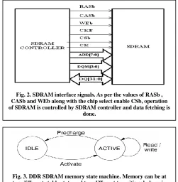
SDRAM signals: RASb Row Address Strobe: Along with /CAS and /WE, this selects one among different commands. It is active low signal which works for row address in the memory.
CASb Column Address Strobe: Along with /RAS and /WE, this selects one of 8 commands. It is active low signal which works for column address in the memory.
WEb Write enable: Along with /RAS and /CAS, this selects one among different commands. This generally
distinguishes read-like commands from write-like
commands. All the above are command bits.
TABLE I
SDRAM COMMAND WITH STROBE SELECT Function Cs RASb CASb WEb Address
Active L L H H Row
Read L H L H Col
Write L H L L Col
Pre-charge L L H L Row
DQ Data lines: This is a bi-directional bus signal on which either a data read or a data write operation is taken at a time. Both operations cannot be taken in parallel. This bidirectional bus carries data to and from the memory.
DQM Data Mask: When high, these signals suppress data I/O. When accompanying write data, the data is not actually written to the DRAM. When asserted high two cycles before a read cycle, the read data is not output from the chip. The masked data remains unchanged and unmasked data is what a master accessed for either a read or a write operation.
III. AHBINTERFACE (ADVANCE HIGH PERFORMANCE
BUS)
[image:2.612.319.570.214.470.2]AHB is a new generation of AMBA bus which is intended to address the requirements of high-performance synthesizable designs. It is a high-performance system bus that supports multiple bus masters and provides high-bandwidth operation. Bridging between this higher level of bus and the current ASB/APB can be done efficiently to ensure that any existing designs can be easily integrated. An AMBA AHB design may contain one or more bus masters, typically a system would contain at least the processor and test interface. However, it would also be common for a Direct Memory Access (DMA) or Digital Signal Processor (DSP) to be included as bus masters.
[image:2.612.50.295.227.426.2]Fig. 1. SYNCHRONOUS DRAM
Fig. 2. SDRAM interface signals. As per the values of RASb , CASb and WEb along with the chip select enable CSb, operation of SDRAM is controlled by SDRAM controller and data fetching is
done.
Fig. 3. DDR SDRAM memory state machine. Memory can be at two different stable state and two different transitional phase in between states as PRECHARGE and ACTIVATE. In an active state memory is ready to get accessed like reading and writing
[image:2.612.54.284.591.650.2]International Journal of Emerging Technology and Advanced Engineering
Website: www.ijetae.com (ISSN 2250-2459,ISO 9001:2008 Certified Journal, Volume 3, Issue 3, March 2013)
909
A. AHB Slave Interface Signals
1. HCLK Bus: Clock source: This clock times all bus transfers. All signal timings are related to the rising edge of HCLK.
2. HRESETn Reset Source: The bus reset signal is active LOW and is used to reset the system and the bus. This is an active LOW signal.
3. HADDR [31:0] (Address bus) Master: The 32-bit system addresses bus.
4. HTRANS [1:0] (Transfer type) Master: Indicates the type of the current transfer, which can be IDLE or BUSY.
5. HWRITE (Transfer direction) Master: When HIGH this signal indicates a write transfer and LOW as read transfer.
6. HBURST [2:0] (Burst type) Master: Four, eight and sixteen beat bursts are supported.
7. HWDATA [31:0] (Write data bus) Master: The write data bus is used to transfer data from the master to the bus slaves during write operations. A minimum data bus width of 32 bits is recommended.
8. HSELx (Slave select) Decoder: Each AHB slave has its own slave select signal and this signal indicates that the current transfer is intended for the selected slave.
9. HRDATA [31:0] (Read data bus) Slave: The read data bus is used to transfer data from bus slaves to the bus master during read operations. A minimum data bus width of 32 bits is recommended. However, this may easily be extended to allow for higher bandwidth operation.
10. HREADY (Transfer done) Slave: When HIGH the HREADY signal indicates that a transfer has finished on the bus. This signal may be driven LOW to extend a transfer.
Note: Slaves on the bus require HREADY as both an input and an output signal
11. HRESP [1:0] (Transfer response) Slave: The transfer response provides additional information on the status of a transfer. Four different responses are provided but for our design we consider OKAY and ERROR as for one master.
12. HBUSREQx (Bus request): Indicates that the bus master requires the bus. There is an HBUSREQx signal for each bus master in the system, up to a maximum of 16 bus masters.
13. HGRANTx : (Bus grant)Arbiter This signal indicates that bus master x is currently the highest priority master.
15: HSPLITx [15:0]: (Split completion) Indicate to the arbiter which bus masters should be allowed to re-attempt a split transaction. Each bit of this split bus corresponds to a single bus master.
IV. MEMORY CONTROLLER IMPLEMENTED DESIGN
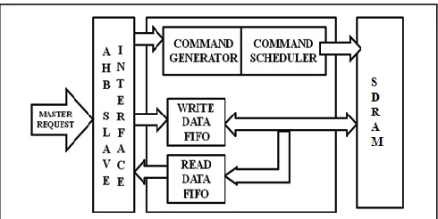
[image:3.612.50.303.132.280.2]Since the processor is faster than the memory, it is illogical to make the processor wait till each command is executed for it to give the next command. So the controller has to have some kind of storage as given in figure above, so that it can buffer multiple requests from the AHB slave interface while the processor continues with other work.
[image:3.612.324.569.421.544.2]Fig. 5. System module. Here in order to reduce the clock cycles of fetching data from memory two FIFO's are used to store and schedule commands that are generated by command generator Fig. 4. AHB Slave Interface Signal Description. AHB works as a
slave for processors and helps them as Masters to communicate with DDR SDRAM memories through Controller hence the input signals
International Journal of Emerging Technology and Advanced Engineering
Website: www.ijetae.com (ISSN 2250-2459,ISO 9001:2008 Certified Journal, Volume 3, Issue 3, March 2013)
910
We used FIFO to store the Read/Write commands coming from processors/user side along with corresponding write data and included a search engine to search recently read/write data inside the FIFO in order reduce the clock cycles of fetching data from SDRAM.
A. SDRAM controller Architecture with FIFO’s in Ping-Pong Fashion
Only one open row in an active bank can be accessed. An ACTIVE command can open a row and make active the particular row in the memory. A PRECHARGE command issued to memory can set the SDRAM to idle state, i.e. closing the open row in this memory. If every time after accessing a row AUTOPRECHARGE command is performed, and the next access is actually involving the same row of the same bank, an ACTIVE command needs to be applied again in order to access last open row.
As it is known that time needed between ACTIVE and READ/WRITE commands has to be fulfilled. In a successive period of time a program probably only accesses a small part of continuous address space. So that it is not necessary to issue an AUTO-PRECHARGE command after every read/write access without judging if there’s any need. If the current access is for an open row in an active bank, the READ or WRITE command is directly issued to the SDRAM, the ACTIVE and READ or WRITE commands.
When the auto-refresh is required, all the active banks will be inactivated by applying PRECHARGE ALL command as auto-refresh can only be issued when the whole SDRAM is in idle state. In this way, the overhead caused by frequently opening and closing the SDRAM banks can be decreased.
The memory controller basically consist of three main sub parts, they are
1) 2 Read and 2 write FIFOs 2) Command generator
3) Command scheduler Read FIFO
It is known that, SDRAM cannot finish the data access in a single cycle. So we need some strategies to decrease the responding time. We analyzed our application and found that if the SDRAM is accessed in the single mode, the needing data is available at least after 2 cycles Plus time consumed by the latching in the bus interface part and the PRECHARGE command, in fact, it is more than 2 cycles. To support the fast response time, burst mode access and read FIFO'ing techniques need to be used whenever possible. When AHB bus needs to read data, see if data is already in read FIFO by only checking if the current accessing address is in the range of either of the read FIFO and if the corresponding bit in the corresponding Valid-Vector is valid. The Valid-Valid-Vector is used to mark if the data stored in data FIFO is valid. Valid-Vector works like tags for a cache.
Every read FIFO is only as big as the capacity of a SDRAM burst, so that Valid-Vector is only a several bit vector. If the needed data is in read FIFO, data can be directly read from them, otherwise, a READ command is needed issuing to SDRAM.
After a preset number of clock cycles, the data is available on the output latches of the SDRAM for reading, and data is delivered to AHB bus and written to one of the read FIFO at the same time. The whole burst access data will be loaded in read FIFO.
In this way, we implemented prefetching. According to the local principles of programs, the next read access is possibly a successive address to the current one. So the next data can be read from read FIFO, which can fasten the responding speed. In order to reduce the complexity of implementing read FIFO, data from SDRAM are stored in read FIFO 0 and read FIFO1 in turn.
B. Ping-Ponging fashion of writing:
As it is described about the AHB, in order to reduce the responding time to write access, write FIFO are used to pack and align the data when the AHB bus data transfer size does not match the SDRAM data bus width. Based on our previous research on FPGA designs, we didn’t use only one write FIFO, instead, we use 2 FIFO. It is well known that ping-ponging can reduce or eliminate the mismatch effects between 2 different modules which are operating at different speeds.
Fig.6. Proposed architecture of SDRAM controller. Here two read and two write FIFO's can store four address and four
International Journal of Emerging Technology and Advanced Engineering
Website: www.ijetae.com (ISSN 2250-2459,ISO 9001:2008 Certified Journal, Volume 3, Issue 3, March 2013)
911
By utilizing ping-ponging between the two write FIFO, part of the time writing one FIFO and part of the time moving data from another FIFO to off chip SDRAM can be overlapped.
If write FIFO 0 is not empty and write FIFO 1 is being written by AHB bus, move FIFO 0’s data to SDRAM and this FIFO will be in the progress of moving until all data is moved to SDRAM, vice versa. This is the ping-ponging technique we used between write FIFO 0 and write FIFO 1. The flow of moving data from FIFO to SDRAM is as follows:
If write FIFO 0 is empty, data will be written to write
FIFO 0
Else if write FIFO 1 is in the progress of AHB writing
and write If write FIFO 0 is being written by AHB bus and write FIFO 1 is not empty, move FIFO 1’s data to SDRAM and if FIFO 0 is not empty, move FIFO 0’s data to SDRAM.
This flow explains how the ping-ponging works as memory buffering and make the time writing FIFO and writing SDRAM to overlap. The description of operations about AHB bus writing FIFO is as follows:
1. If write FIFO 0 is empty, data will be written to write FIFO 0.
2. Else if write FIFO 0 is not empty or in the progress of moving its data to SDRAM and if write FIFO 1 is empty, data will be written to write FIFO 1.
3. Else make the AHB bus hold the bus signals until one of the FIFO is empty.
C. Read Update Logic:
One of the novel features of this controller is read update logic. When the controller encounters a read command at the head of the FIFO queue, it takes this command and searches the FIFO to see if the required data is already in the FIFO. This search is carried out in parallel and all the FIFO locations are searched in one clock cycle. Hence the searching time is not dependent on the depth of the FIFO but at the cost of hardware overhead. Once the data is found in the FIFO, which was the result of a previous operation, it is directly routed to the output. Hence saving the time and burden of fetching it from the DRAM memory.
If the data is not found in the FIFO then the controller executes the request on the memory as usual. Thus if the data is found internally then we save a lot of clock cycles, but even if the data is not found internally then we just lose one clock cycle.
TABLE III
COMMAND GENERATOR POSSIBLE STATES
Scenario 1: Y=null ROW EMPTY
Scenario2: X==Y ROW HIT
Scenario 3: X!=Y
ROW CONFLICT
ACT X RD/WR X PRE Y
RD/WR ACT X
RD/WR X
Where X=Requested address by master Y=Current address in the activated row buffer
1. ROW EMPTY (RE):For any read/write operation check for the row buffer status, if f the row buffer is empty then directly go for activating the row buffer by the command ACT from the command generation and then perform the requested read or write operation on the row buffer by giving the RD/WR command.
2: ROW HIT (RH): For any read/write operation check for the row buffer status, if f the requested address corresponds the same row which is already activated in the row buffer for any previous transfer, then directly perform the requested read or write operation on the row buffer by giving the RD/WR command.
3: ROW CONFLICT (RC): For any read/write operation check for the row buffer status, if the requested address differs from the row which is already activated in the row buffer for any previous transfer, then pre-charge the existing row in the row buffer by giving the PRE command and then activate the requested address row by the ACT command and perform the requested read or write operation on the row buffer by giving the RD/WR command.
International Journal of Emerging Technology and Advanced Engineering
Website: www.ijetae.com (ISSN 2250-2459,ISO 9001:2008 Certified Journal, Volume 3, Issue 3, March 2013)
912
1. RD to RD in row hit scenario 2. RD to RD in row conflict scenario 3.RD to WR in row hit scenario 4.RD to WR in row conflict scenario
The second condition is, if the present state is a write there exist four combinations of operations that has to be taken,
1. WR to WR in row hit scenario 2.WR to WR in row conflict scenario 3.WR to RD in row hit scenario 4.WR to RD in row conflict scenario
D. Updated Memory Controller FSM
V. SIMULATION RESULTS
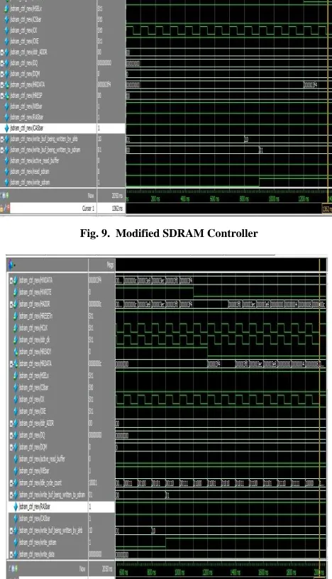
[image:6.612.52.287.127.272.2]A. Modified SDRAM Controller with FIFOing
[image:6.612.323.563.156.437.2]Fig. 9. Modified SDRAM Controller
[image:6.612.326.560.207.615.2]Fig. 10. Modified SDRAM Controller continued Fig. 7. Command Generator State Machine. This is state
machine for command generator that is defined considering the normal working of SDRAM controller without updating.
Fig. 8. Command Generator State Machine. This is state machine for command generator that is defined considering all probable
[image:6.612.50.294.463.647.2]International Journal of Emerging Technology and Advanced Engineering
Website: www.ijetae.com (ISSN 2250-2459,ISO 9001:2008 Certified Journal, Volume 3, Issue 3, March 2013)
913
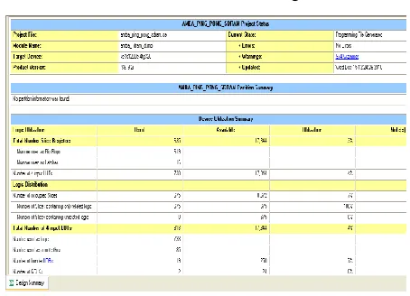
V. SYNTHESIS REPORT
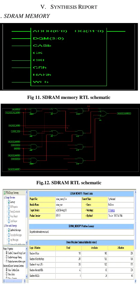
[image:7.612.53.287.116.591.2]A. SDRAM MEMORY
Fig 11. SDRAM memory RTL schematic
Fig.12. SDRAM RTL schematic
Fig. 13. SDRAM memory synthesis report
B. SDRAM Controller (without FIFOing)
[image:7.612.324.563.133.385.2]Fig. 14. SDRAM CONTROLLER RTL schematic
Fig. 15. SDRAM CONTROLLER RTL schematic C. Modified SDRAM Controller with FIFOing
Fig. 16. SDRAM CONTROLLER RTL schematic Synthesis Options Summary
Source Parameters
1. Input File Name: "amba_sdram_dump.prj" 2. Input Format: mixed
International Journal of Emerging Technology and Advanced Engineering
Website: www.ijetae.com (ISSN 2250-2459,ISO 9001:2008 Certified Journal, Volume 3, Issue 3, March 2013)
914
HDL Compilation
1. Compiling verilog file "memory.v" in library work 2. Compiling verilog file "sdram_ctrl_new_ping_pong.v" in library work
3. Module <sdram_mem> compiled
4.Compiling verilog file
"amba_ping_pong_sdram_dump.v" in library work 5. Module <sdram_ctrl_new_ping_pong> compiled 6. Module <amba_sdram_dump> compiled No errors in compilation
7. Analysis of file <"amba_sdram_dump.prj"> succeeded.
Design Hierarchy Analysis
1. Analyzing hierarchy for module <amba_sdram_dump> in library <work>.
2.Analyzing hierarchy for module
<sdram_ctrl_new_ping_pong> in library <work> with parameters.
RESET = "000" ACTIVE = "001" ACTIVE1 = "010" ACTIVE2 = "011" READ = "100" WRITE = "101" PRECHARGE1 = "110" PRECHARGE2 = "111"
3. Analyzing hierarchy for module <sdram_mem> in library <work>.
Final Results
1.RTL Top Level Output File Name:
amba_sdram_dump.ngr
2. Top Level Output File Name: amba_sdram_dump 3. Output Format: NGC
4. Optimization Goal: Speed 5. Keep Hierarchy: NO
Timing Summary
1. Minimum period: 8.743ns (Maximum Frequency: 114.383MHz)
2. Minimum input arrival time before clock : 6.914ns 3. Maximum output required time after clock : 10.075ns 4. Maximum combinational path delay : No path found
Timing Detail
All values displayed in nanoseconds (ns)
1. Timing constraint: Default period analysis for Clock 'clk_count_261'
2. Clock period : 8.743ns (frequency: 114.383MHz) 3. Total number of paths / destination ports: 16101 / 1162 4. Delay: 8.743ns (Levels of Logic = 5)
5. Source: mc0/write_buf_write_pointer_1_1 (FF) 6. Destination: mc0/write_addr_buf<1>_3_31 (FF) 7. Source Clock : clk_count_261 rising
[image:8.612.330.557.267.431.2]8. Destination Clock: clk_count_261 rising
Fig. 17. Synthesis Result modified SDRAM
Testing results between our controller and the traditional controller, the speedup rate difference is 2.1ns. Moreover, for the two SDRAM controllers, we compared the times of issuing READ and WRITE commands to off chip SDRAM while running the application program. running the same application program, modified SDRAM controller can reduce the times of accessing off chip SDRAM, which has a heuristic meaning for low power designs as well.
International Journal of Emerging Technology and Advanced Engineering
Website: www.ijetae.com (ISSN 2250-2459,ISO 9001:2008 Certified Journal, Volume 3, Issue 3, March 2013)
915
TABLE III
CONSTRAINTS COMPARED IN ORIGINAL AND NEW CODE AFTER SIMULATION
Compared Constraints of Original and Modified SDRAM
Original Memory Controller (SDRAM)
Modified Memory Controller (SDRAM)
Maximum combinational path Latency
11.460ns No path found Maximum Frequency 92.319MHz 114.383MHz
Minimum input arrival time before clock
9.902ns 6.914ns
Minimum period 10.832ns 8.743ns
Minimum input arrival time before clock
9.902ns 6.914ns
VI. SCOPE SUGGESTONS AND ADVANTAGES
1. Consumes less power hence specially suited for notebook computers, in smart phones where excess of data storage and accessing takes place, Video applications requiring video memory, High speed device with less latency and excess of data storage and accessing takes place.
2. The high performance AMBA AHB interface is used for the speed compatibility between master and the memory. 3. Memory access time is getting reduced because of the latency reduced by 91.66% after the design is used.
4. It has the capacity to transfer data 64 bits at a time at 100 MHz bus frequency.
5. It also supports burst transfer of the data, masking. 6. Chip achieves less area as we use DRAMs that has only one transistor and one capacitor.
VII. CONCLUSION
We are modifying our memory controller by helping its SDRAM buffer through two FIFO's are used one for transmitting and other for receiving data also referred as PING_PONG FIFO'ing. Two FIFO's are writing and other two for reading. These FIFO's are used to change the flow of command generator operation. As without FIFO the command generator directly communicates with memory but in updated logic command generator and scheduler use FIFO's for scheduling and queuing the commands.
For a master that hands its request to interface, transaction is completed at the moment the request in handover to controller and bus is free. Thus not only the SDRAM memory is getting efficient but AHB bus utilization also enhances as per our design. Thus by utilizing four FIFO with command generator and command scheduler in controller two operation i.e..FIFO'ing in ping-pong fashion and Read update logic is evaluated that yields in reducing the latency. The testing results shows 91.66% of reduced delay with FIFOing when compared to the latency produced with FIFOing t, which is nothing but the in-built memory used within the SDRAM controller to improve its performance.
REFERENCES
[1] ―AMBA Specification (Rev2.0)‖, ARM Inc.
[2] ARM. ―AMBA Open Specifications‖
http://www.arm.com/products/system-ip/amba/amba-openspecifications.php
[3] Hu Yueli,Yang Ben "Building an AMBA AHB compliant Memory Controller‖ in 2011.
[4] http://infocenter.arm.com/help/topic/com.arm.doc
[5] ―PrimeCell AHB SRAM/NOR Memory Controller‖, Technical Reference Manual, ARM Inc.
[6] Micron Technology Inc. Synchronous DRAM Data Sheet, 2001. [7] ―Memory Controllers for Real-Time Embedded systems‖
BennyAkesson Kees Goossens vol. 3, no. 3, pp. 75–77, Mar1999. [8] Samir Palnitkar, Pearson 2nd edition ―Verilog HDL, A Guide to
Digital Design and Synthesis.
[9] Double Data Rate (DDR) SDRAM Specification,JEDEC
International Journal of Emerging Technology and Advanced Engineering
Website: www.ijetae.com (ISSN 2250-2459,ISO 9001:2008 Certified Journal, Volume 3, Issue 3, March 2013)
916
AUTHORBIOGRAPHY
[1] Mrs. Archana Chandrikaram Sharma is pursuing M.Tech. from Disha Institute of Management and Technology , Raipur (India) in Electronics and Telecommunication Engineering (VLSI & Embedded System Design). She is having 3 year of teaching experience and 1 year of industrial experience.