IN ORGANIC SOLAR CELL DEVICE
MUHAMAD YUSUF BIN ZULKEFLY
A project report submitted in partial fulfillment of the requirement for the award of the
Degree of Master of Electrical Engineering
Faculty of Electrical and Electronic Engineering Universiti Tun Hussein Onn Malaysia
v
ABSTRACT
Organic solar cell device has become one of the most promising ways to tackle today's energy issue by offering low production cost, light weight, mechanically
flexible and possibility of large area fabrication. Poly(3-hexylthiophene) (P3HT) and [6,6]-phenyl C61-butyric acid methyl ester (PCBM) blends is the most efficient fullerene derivative based donor-acceptor copolymer so far. Current conventional organic solar cell (OSC) device consist of active layers (donor and acceptor) sandwiched by indium tin oxide (ITO) (a high work function, transparent metal oxide) as the anode and low work function metal such as aluminum (Al) as cathode.
The recent power conversion energy (PCE) has reached as high as 7.4%. But in spite of high PCE, this device suffers from degradation due to sensitivity of low work function metal to oxygen and moisture in air. An inverted structure of organic solar cell (OSC) device with active layers (donor and acceptor) sandwiched by indium tin oxide (ITO) as the cathode and much higher work function metal and more air stable
such as aurum (Au) or silver (Ag) as back contact is an alternative solution to improve the durability. However, ITO is not suitable for electron collection due to large energy band gap between acceptor PCBM and ITO. By introducing thin buffer layer of titanium dioxide (TiO2) between ITO and PCBM may improve overall efficiency of the inverted structure OSC because the new suggested interlayer provide efficient pathway for electrons collections. The aim of this research is to
ABSTRAK
Sel solar organik telah menjadi salah satu kaedah yang paling sesuai untuk mengatasi masalah tenaga pada masa kini dengan menawarkan faedah kos pengeluaran yang
rendah, ringan, jasad yang fleksibel dan kemungkinan fabrikasi kawasan yang luas. Campuran poly(3-hexylthiophene) (P3HT) dan [6,6]-phenyl C61-butyric acid methylester (PCBM) merupakan fullerene terbitan paling berkesan berasaskan penderma-penerima kopolimer setakat ini. Sel solar organik konvensional semasa terdiri daripada lapisan aktif (penderma-penerima), diapit oleh indium tin oxide (ITO) (sejenis oksida logam telus yang mempunyai fungsi kerja yang tinggi) sebagai
anod dan logam yang mempunyai fungsi kerja rendah seperti aluminum (Al) sebagai katod. Kecekapan semasa telah mencecah 7.4%. Walaupun angkanya agak tinggi, peranti ini mengalami masalah degradasi disebabkan oleh sensitiviti logam berfungsi kerja rendah terhadap oksigen dan kelembapan udara. Struktur terbalik sel solar organik yang terdiri daripada lapisan aktif (penderma-penerima), diapit oleh ITO
sebagai katod dan logam berfungsi kerja tinggi dan lebih stabil terhadap udara seperti emas (Au) dan perak (Ag) sebagai anod adalah jalan alternatif untuk meningkatkan ketahanan. Namun begitu, ITO tidak sesuai sebagai pengumpul elektron kerana beza fungsi tenaga kerja yang besar antara penerima PCBM dan ITO. Dengan memperkenalkan lapisan penampan titanium dioxide (TiO2) diantara ITO dan PCBM bakal meningkatkan kecekapan sel solar organik terbalik secara
vii
CONTENTS
TITLE i
DECLARATION ii
DEDICATION iii
ACKNOWLEDGEMENT iv
ABSTRACT v
CONTENTS vii
LIST OF TABLES x
LIST OF FIGURES xi
LIST OF SYMBOLS AND ABBREVIATIONS xiii
LIST OF APPENDICES xiv
CHAPTER 1 INTRODUCTION 1
1.1 Introduction to organic solar cell (OSC) 1
1.2 Problems Statement 3
1.3 Research Objectives 4
1.5 Project report outline 5
CHAPTER 2 LITERATURE REVIEW 6
2.1 Background history 6
2.2 Organic solar cell's efficiency model 8
2.3 Titanium dioxide (TiO2) 10
2.4 Sol gel method 11
2.5 Fabrication tools 11
2.5.1 Spin coater machine 12
2.5.2 Magnetic stirrer machine 12 2.5.3 Ultrasonic bath cleaner 13
2.5.4 Annealing chamber 14
2.5.5 Sputter coater 14
2.6 Characterization and measurement tools 15
2.6.1 FESEM/EDS machine 15
2.6.2 AFM machine 16
2.6.3 Surface profiler 17
2.6.4 I-V characteristic with solar simulator 17
CHAPTER 3 METHODOLOGY 18
3.1 Basic OSC device fabrication 18 3.2 Proposed OSC device fabrication 23
CHAPTER 4 RESULTS AND DISCUSSION 33
4.1 Results and discussion 33
4.1.1 EDS 33
4.1.2 FESEM 42
4.1.3 AFM 45
4.1.4 I-V characteristic 46 4.1.4.1 Basic OSC device 46
ix
CHAPTER 5 CONCLUSION AND DISCUSSION 53
5.1 Conclusion 53
5.2 Future Recommendation 53
REFERENCES 55
LIST OF TABLES
4.1 Chemical composition of materials for sample A 35 4.2 Chemical composition of materials for sample B 38
xi
LIST OF FIGURES
1.1 Cross section structure of basic OSC 2 1.2 OSC's microscopic working mechanism 2
1.3 Cross section of basic inverted OSC 3 1.4 Energy level diagram of materials in basic inverted OSC 3
2.1 I-V curve of solar cell 9
2.2 Graphical illustration of FF determination 9 2.3 Spin coater taken from MiNT-SRC, UTHM 12 2.4 Magnetic stirrer taken from MiNT-SRC, UTHM 13
2.5 Ultrasonic bath taken from MiNT-SRC, UTHM 13 2.6 Annealing chamber taken from MiNT-SRC, UTHM 14 2.7 Sputter coater taken from MiNT-SRC, UTHM 15 2.8 FESEM/EDS machine taken from MiNT-SRC, UTHM 16 2.9 AFM machine taken from MiNT-SRC, UTHM 16
2.10 Surface profiler taken from MiNT-SRC, UTHM 17 2.11 I-V characteristic measurement with solar simulator
taken from MiNT-SRC, UTHM 17
3.1 Cross section of basic inverted OSC 19 3.2 Basic inverted OSC device process flow 19 3.3 Cross section of proposed inverted structure OSC 21
3.4 Proposed inverted OSC device process flow 21 4.1 Electron image of materials deposited on sample A 34
4.2 EDS spectrum of sample A 35
4.3 Electron image of materials deposited on sample B 37
4.4 EDS spectrum of sample B 38
4.5 Electron image of materials deposited on sample C 39
4.7 FESEM image of sample A 42
4.8 FESEM image of sample B 43
4.9 FESEM image of sample C 44
4.10 AFM topography of sample D 45
4.11 AFM topography of sample E 46
4.12 Basic OSC device assembly and testing 47 4.13 IV characteristic curve of basic OSC device 47 4.14 Zoomed in graph IV curve of basic OSC device 48 4.15 Power output curve of basic OSC device 49 4.16 Proposed OSC device assembly and testing 50
xiii
LIST OF SYMBOLS AND ABBREVIATIONS
OSC - organic solar cell PV - photo voltaic
Al - aluminum
ITO - indium tin oxide
P3HT - poly (3-hexylthiophene)
PCBM - phenyl C61-butyricacid methyl ester PCE - power conversion efficiency
Au - aurum/gold
LUMO- lowest unoccupied molecular orbid HOMO - highest occupied molecular orbid eV - electron volt
TiO2 - titanium dioxide
UTHM- University Tun Hussein Onn Malaysia
Ag - silver
MPP - maximum power point Pmax - maximum power VOC - open circuit voltage ISC - short circuit current Imp - maximum current
Vmp - maximum voltage FF - fill factor
PT - theoretical power
EDS - energy dispersive spectroscopy
LIST OF APPENDICES
APPENDIX TITLE PAGE
CHAPTER 1
INTRODUCTION
1.1 Introduction to organic solar cell (OSC)
Solar cell is a device that converts radiation of sunlight into electricity. Harnessing solar energy is one of the most promising ways to tackle today's energy issue. The present dominant photovoltaic (PV) technology is based on inorganic materials. High material and manufacturing cost limits its wide acceptance. Intensive research has been conducted towards the development of low cost PV technology of which
organic photovoltaic (OPV) device are one of the promising OPV device.[1-3] Organic photovoltaic (OPV) or organic solar cell (OSC) is a subset of solar cell consisting of conjugate polymer and bulk heterojunction composites. OSC have attracted much attention for renewable energy due to their promising properties such as low production cost, lightness, light weight, mechanical flexibility and the possibility of large area fabrication. [4-6]
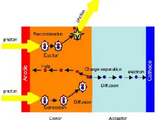
Figure 1.1: Cross section structure of basic OSC
The microscopic working steps of an OSC generally operate through four (4) major steps. The first step is absorption of incidents photons which is affected by surface property. The second step involves excitons production in OSC active layer. Excitons is an electron-hole pair and the production is determined by the material's band structure. The third step is the separation of the pairs, determined by the charge
distribution inside the cell. The final step happens after the electrons and holes was collected at electrodes.[8] This process can be illustrated as in figure 1.2.
Figure 1.2: OSC's microscopic working mechanism
Organic solar cells promise for low cost energy production but are yet far to be realized in practical world. There are some challenges that need to be considered as issues. Problems such as low efficiency and short lifetime are yet to be solved. Organic solar cell device has become one of the most promising way to tackle
[image:13.612.241.400.443.564.2]3
1.2 Problems statement
Inverted organic solar cell architecture are very attractive for manufacturability and improved device lifetime but the Indium Tin Oxide (ITO) as a cathode are not well
suited as an electron selective electrode.[8-13].
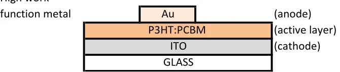
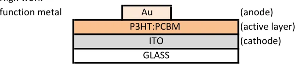
High work
function metal Au (anode)
(active layer) (cathode) P3HT:PCBM
[image:14.612.155.490.212.283.2]ITO GLASS
Figure 1.3: Cross section of basic inverted OSC
Figure 1.3 shows the cross section of materials in inverted OSC where glass coated Indium Thin Oxide (ITO) act as cathode, high work function metal such as aurum, Au as the metal anode and the active layer used is blend polymer donor-acceptor P3HT:PCBM. (P3HT - poly(3-hexylthiophene), PCBM - phenyl C61-butyric acid methyl ester). Most bulk heterojunction OSCs use
poly(3-hexylthiophene) (P3HT) as the conjugated polymer and [6,6]-phenyl C-butyric acid methyl ester (PCBM) as the fullerene derivative.\ A power conversion efficiency (PCE) over 5% has recently been obtained using these kinds of materials. [14]
-3.0eV LUMO
-3.8eV LUMO (lowest unoccupied
LUMO molecular orbit)
-4.7eV -5.1eV HOMO
-5.3eV (Highest occupied
-6.1eV HOMO moleculR orbit)
HOMO
ITO PCBM P3HT Au
[image:14.612.190.456.501.653.2](cathode) (accpetor) (donor) (anode)
The detail microscopic working mechanism in inverted organic solar cell can be explain from energy level diagram of figure 1.4. After absorption of incidents photons, excitons (pair of electron-hole) are produce in active layer (P3HT:PCBM). Separation of the pairs and collections of electrons and holes at electrodes are then required to ensure the conductivity of electricity in the cells. Electrons from donor
material (P3HT) will travel from its LUMO band to ITO cathode through LUMO of PCBM and holes was collected at metal anode, Au from HOMO band of acceptor material (PCBM) through HOMO band of P3HT. However ITO is not suitable for electron collective electrode due to the large gap of electron volts (eV) between ITO and LUMO level of PCBM.
1.3 Research objectives
The aim of this research is to fabricate inverted organic solar cell device consisting
of ITO/P3HT:PCBM/Au and introduce thin layer of Titanium Dioxide (TiO2) as an electron collecting layer between ITO and P3HT:PCBM using sol gel method at room temperature to improve the performance of the device.
(i) To investigate the effect of introducing TiO2 buffer layer TiO2 between
P3HT:PCBM layer and ITO cathode in inverted OSC. (ii) To fabricate OSC device using optimum TiO2solution. (iii) To characterize OSC device with TiO2buffer layer.
1.4 Scopes of project
The scope or works performed throughout this project are as describe below:
5
(ii) To identify and prepare appropriate TiO2 solution to be used in sol gel method.
(iii) To coat TiO2 buffer layer onto polymer blend P3HT:PCBM active layer optimized by research group UTHM.
(iv) To fabricate inverted OSC with and without TiO2 interlayer using sol gel
method at room temperature.
(v) To measure, characterize and examine fabricated devices’ surface topology, I-V characteristic using appropriate machine.
(vi) To make comparison and analysis study between fabricated OSC with and without TiO2interlayer
1.5 Project report outline
This project report consists of 5 main chapters, and organized as follows:
Chapter 2 brief overview of organic solar cell and explanation on mathematical theory of solar cell. Electrical characterization for standard OSC devices will be also included in this chapter. Chapter 3 describes material and experimental methods involved in this project. Chapter 4 describes process optimization result and electrical characterization of OSC
LITERATURE REVIEW
This chapter describes the historical timeline and technology development of organic solar cell (OSC), briefing of materials, fabrication tools and characterization equipment. This chapter may help in understanding this project through basic
theories.
2.1 Background history
The discovery of the photovoltaic (PV) effect is commonly ascribed to Becquerel, who discovered a photocurrent when platinum electrodes, covered with silver bromide or silver chloride, was illuminated in aqueous solution. Smith and Adams made the first reports on photoconductivity, in 1873 and 1876, respectively, working on selenium. Anthracene was the first organic compound which photoconductivity
was observe by Pochettino in 1906 and Volmer in 1913.[2]
In the late 1950s and 1960s the potential use of organic materials as photoreceptors in imaging system was recognized. In the early 1960s it was discovered that many common dyes such as methyene blue, had semiconducting properties. Later, these dyes were among the first organic materials to exhibit the PV effect. However, simple PV devices based on dyes or polymer yield limited power
7
A major breakthrough came in 1986 when Tang discovered that bringing donor and an acceptor together in one cell could dramatically increase the PCE to 1%. Earlier problems in obtaining efficient charge carrier separation have been overcome and PCE more than 3% have been reported. Some of the next most important milestone in the development of organic solar cells are Hiramoto whom
made the first dye/dye bulk heterojunction PV by co sublimation in 1991, Sariciftci whom made the first polymer/C60 heterojunction device in 1993, Yu whom made the first bulk polymer/c60 heterojunction PV in 1994, Yu and Hall whom made the first bulk polymer/polymer heterojunction PV in 1995, Peter / van Hal whom used olingomer-C60 dyads/triads as the active material in PV cells in 2000,
Schmidt-Mende whom made a self organized liquid crystalline solar cell of hexabenzocoronene and prylene in 2001, and the usage of double-cable polymers in PV cells by Ramos in 2001. [2]
The most common strategy to maximize the efficiency of OSC devices is to mix the donor and acceptor materials in an optimum composition leading to a bulk heterojunction (BHJ) device. In a normal structured OSC device, the active layer
(ActL) of donor–acceptor blend is sandwiched between the indium tin oxides or ITO (anode) coated on the glass substrate and a low work function metal. One major impediment for OSC devices is their poor environmental stability resulting in fast device degradation and hence short life times. [17]
One of the suggested way to improve the life times of OSC devices is to use
an inverted device structure in the form glass/ITO/ETL/ActL/HTL/Ag or Au (ETL: electron transport layer, ActL: active layer) where ITO electrode is used for electron collection (cathode) while the top electrode is made of a high work function metal such as Ag or Au serving as anode for hole collection. Consequently, the charge transport in this device structure is opposite to that in the normal device structure. This layer stacking sequence is believed to provide superior ambient stability of the
device in comparison to the devices using Al electrodes and PEDOT:PSS as HTL. [18]
Recent the power conversion efficiency (PCE) of the bulk heterojunction polymer solar cells has reached as high as 7.4% in conventional device structures. Conventional organic photovoltaic, OPVs generally consist of active layers sandwiched by a high work function and transparent metal oxide as the anode such
PCE, the conventional OPVs can suffer from degradation of the cathode due to their sensitivity to oxygen and moisture in air. Therefore, the devices in this structure exhibit short lifetime. [19]
In order to overcome these problems, the inverted device structures is an alternative solution to improve the durability, because it uses a more air-stable high
work function electrode such (Ag, Au) as back contact to collect holes while using an inorganic semiconductor for buffer layer to collect electrons. The usage of inorganic semiconductor embedded into the conjugated polymer have several attributes as electron acceptors, including relatively high electron mobility, high electron affinities, hole-blocking ability and good physical and chemical stability.[20]
In this work the fabrication of inverted polymer solar cells and investigate the role of thin dense metal oxide films in the inverted polymer solar cells using dense film of TiO2and Nb2O5. These two oxides were purposely selected in view of the bottom of conduction band of TiO2 lower than the LUMO level of PCBM and that of Nb2O5higher than the LUMO level of PCBM. It was found that a very thin metal oxide films between the electron collecting electrode and active layers was
necessary to promote the formation of continuous uniform PCBM film and thus block the holes in P3HT from being recombined with the electrons in collecting electrode.[4]
2.2 Organic solar cell's efficiency model
There are several microscopic descriptions available modeling the optical and electrical processes in bulk heterojunction solar cells. Those models provide a detailed insight into the performance limiting processes. To calculate the power
conversion efficiency (PCE) of an actual solar cell, several parameters must be determined such as open circuit voltage (VOC), short circuit current (ISC) and electrical fill factor (FF). The open circuit voltage (VOC) is the maximum voltage available when no current is flowing through the solar cell. Short circuit current (ISC) on the other hand is the current through when the voltage across the solar cell is zero. While fill factor (FF) is defined as the ratio of maximum power to the product of VOC
9
Figure 2.1: I-V curve of solar cell
Maximum power output of a solar cell, Pmax often referred to as maximum power point (MPP) is the point where the cell is generating its maximum power.
Voltage and current at that point is referred as Vmp and Imp as shown in figure 2.1 above.
Figure 2.2: Graphical illustration of FF determination
[image:20.612.199.459.431.611.2]theoretical power, PT (total green area or VOC x ISC) as shown in figure 2.2 above. The mathematical equation of fill factor can be written as:
max mp mp
T OC SC
V
xI
P
FF
P
V
xI
(2.1)Efficiency,ŋ is the ratio of electrical power output POUT compared to solar power input, PIN. POUTcan be taken to be Pmax, while PINis taken as the product of
the radiance of the incident light equal to 1000W/m2 or 100 mW/cm2. The mathematical equation of power conversion efficiency,ŋ:
max
(% )
100
mp mp100
OC SC100
in in in
V
xI
P
V
xI
xFF
x
x
x
P
P
P
(2.2)2.3 Titanium dioxide (TiO2)
Titanium dioxide (TiO2) is a white solid inorganic substance that is thermally stable, non-flammable, poorly soluble and not classified as hazardous according to the United Nations (UN) Globally Harmonized System of Classification and Labeling of Chemicals (GHS). TiO2, the oxide of the metal titanium, occurs naturally in several
kinds of rock and mineral sands. Titanium is the ninth most common element in the earth's crust and is typically thought of as being chemically inert.
Titanium dioxide has been used for many years in a vast range of industrial and consumer goods including paints, coating, adhesives, paper and paperboard, plastics and rubber, printing inks, coated fabrics and textiles, catalyst system,
ceramics, floor coverings, roofing materials, cosmetics and pharmaceuticals, water treatment agents, food colorants, automotive products and many more.
11
photocatalytic properties as well as high transparency, excellent mechanical and chemical durability in the visible and near infrared region of spectrum.[22]
2.4 Sol gel method
The idea behind sol gel synthesis is to dissolve the compound in a liquid in order to bring it back as a solid in a controlled manner. Multi component compounds may be prepared with a controlled stoichiometry by mixing sols of different compounds.
This method also enables mixing at an atomic level, results in small particles, which are easily sinter able.
This method was developed in the 1960s mainly due to the need of new synthesis methods in the nuclear industry. A method was needed where dust was reduced (compared to the ceramic method) and which needed a lower sintering temperature. Sol gel synthesis may be used to prepare materials with a variety of
shapes, such as porous structure, thin fibers, dense powders and thin films.
A sol is a dispersion of the solid particles (~0.1-1 µm in a liquid where only the Brownian motions suspend the particles. A gel is a state where both liquid and solid are dispersed in each other, which presents a solid network containing liquid components. The sol gel coating process usually consists of 4 steps:
(i) desired particles once dispersed in a liquid to form a sol
(ii) deposition of sol solution produces the coatings on the substrates by spraying, dipping or spinning.
(iii) particles in sol are polymerized through the removal of the stabilizing components and produce a gel in a state of a continuous network.
(iv) final heat treatments pyrolyze the remaining organic or inorganic components
2.5 Fabrication tools
Several equipments and tools used in sol gel method are as shown below:
2.5.1 Spin coater machine
Spin coater machine are used to coat a substrate with a uniform thin film materials.
The thickness of the materials can be varied by controlling spin coater machine's
[image:23.612.231.420.358.499.2]speed and time. Material’s thickness also may vary depending on materials types itself, solution's concentration, solution's drop quantity or user's spin coating technique (either spin-drop or drop-spin)
Figure 2.3: Spin coater taken from MiNT-SRC, UTHM
2.5.2 Magnetic stirrer machine
13
Figure 2.4: Magnetic stirrer taken from MiNT-SRC, UTHM
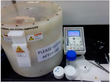
2.5.3 Ultrasonic bath cleaner
Ultrasonic cleaner is a cleaning device that uses ultrasound (usually from 20-400 kHz) and an appropriate cleaning solvent to clean dedicated items. It uses cavitations
bubbles induced by high frequency pressure (sound waves) to agitate a liquid. The agitation produce high forces on contaminants adhering to substrates like metals, plastics, glass, rubber and ceramics. The device also penetrates blind holes, cracks and recesses to remove all traces of contamination.
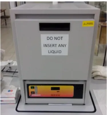
[image:24.612.233.418.504.670.2]2.5.4 Annealing chamber
Annealing is a heat treatment, involves heating a material to above its critical temperature, maintain a suitable temperature and then cooling. It can induce
[image:25.612.232.419.220.421.2]ductility, soften material, relieve internal stresses, refine structure by making it homogeneous and improve cold working properties.
Figure 2.6: Annealing chamber taken from MiNT-SRC, UTHM
2.5.5 Sputter coater
Sputter coating is a sputter deposition process to cover a substrate with a thin layer of
15
Figure 2.7: Sputter coater gold/platinum taken from MiNT-SRC, UTHM
2.6 Characterization and measurement tools
2.6.1 FESEM/EDS machine
This is a Field Emission Scanning Electron Microscope (FESEM) equipped with Energy Dispersive Spectroscopy (EDS). FESEM features allows imaging metallic and ceramic based materials that produce image of a sample by scanning it with a focused beam of electrons which contain information about the sample's surface
Figure 2.8: FESEM/EDS taken from MiNT-SRC, UTHM
2.6.2 AFM machine
AFM stands for Atomic Force Microscope. AFM provide picture of atoms on or in surfaces. Like Scanning Electron Microscope (SEM), the purpose of AFM is to look at the objects on the atomic level, provide higher resolution, does not need to operate in vacuum.
[image:27.612.230.422.537.675.2]17
2.6.3 Surface profiler
Alpha-Step IQ surface profiler is a high measurement precision. This device is ideal for semiconductor pilot lines and materials research. The profiler provides 2D
[image:28.612.249.435.221.345.2]surface profiling analysis and determines thin step height, surface micro roughness and overall form error on thin film surface coatings.
Figure 2.10: Surface profiler taken from MiNT-SRC, UTHM
2.6.4 I-V characteristic measurement with solar simulator
The illuminated current versus voltage (I-V) characteristics of a photovoltaic device typically measured with respect to standard reference conditions. They are defined by the spectrum, intensity, temperature and area.
[image:28.612.246.406.547.669.2]METHODOLOGY
In this chapter, the methodology part will emphasize on process and procedure carried out during preparation and fabrication of organic solar cell device.
3.1 Basic OSC device fabrication
Basic inverted structure organic solar cell (OSC) device fabricated consist of glass
coated Indium tin oxide (ITO) as cathode, organic layer of P3HT:PCBM as active layer and high work function metal Aurum as anode back contact as shown in figure 3.1 and the overall process can be summarized as figure 3.2 below.
High work
function metal Au (anode)
(active layer) (cathode) P3HT:PCBM
[image:29.612.169.477.562.630.2]ITO GLASS
19
Start
P3HT:PCBM solution preparation
Substrate/sample preparation
Active layer coating process, drop-spin P3HT:PCBM solution onto
sample
Pre heat sample at 60ºC for 5 minutes then slow cooling at room
temperature
Anneal sample at 150ºC for 10 minutes then slow cooling at room
temperature
Deposit gold (Au) onto sample
Assembly and testing
End
[image:30.612.239.413.62.488.2]Thickness measurement
Figure 3.2: Basic inverted OSC device process flow
Details of the works procedure are discussed as the following:
(i) Active layer (P3HT:PCBM) solution preparation:
Step 1: Take 15mg of poly(3hexylthiophene) (P3HT) and 15mg of [6,6]
+ +
15mg P3HT 15mg PCBM 1ml DCB
Step 2: The mixture solution then underwent ageing process where it was kept stirred without heat using magnetic stirrer for 24 hours to allow organic materials mixture to fully diluted into solvent.
mixture solution underwent ageing process for 24 hours
(ii) Substrate/sample preparation:
Step 1: Masking and patterning of 25mm x 25mm glass coated ITO with
resistivity 10Ω from Sigma Aldrich using highly corrosive Hydro Fluoric
acid.
21
Step 2: clean substrate from contamination using ultrasonic bath then blow dry using nitrogen gas
ultrasonic bath clean substrate
(iii) Active layer (P3HT:PCBM) coating process : To coat substrate with active layer, place substrate in spin coater, drop solution onto substrate, wait for several moments to enable solution to seep, then spin using 2-step setting
500rpm for 30 seconds and 1000rpm for 60 seconds.
spin coat active layer
(iv) Pre heat sample at 60ºC for 5 minutes using magnetic stirrer. Then slow cooling at room temperature to pyrolyze any unwanted ingredient other than P3HT:PCBM.
(v) Thickness measurement is then done using Alpha step-Q surface profiler machine. The desired thickness of organic layer is between 70nm to 150nm to avoid any exciton recombination. The measurement are done with the results of 150nm using previous spin coater machine speed.
Alpha-step IQ surface profiler
(vi) Anneal the sample at 150ºC for 10 minutes then apply slow cooling at room temperature.
23
(vii) Deposit high work function metal Aurum (Au) onto other material using sputter coater as the back contact with setting current 40mA for 200 seconds.
sputter coater Au deposited on back contact
(viii) Assemble all samples by attaching back contact onto substrate for further testing.
completed device
3.2 Proposed OSC device fabrication
New inverted structure organic solar cell (OSC) device fabricated consist of glass coated Indium tin oxide (ITO) as cathode, titanium dioxide (TiO2) as buffer layer, P3HT:PCBM as active layer and high work function metal Aurum as anode back
High work
function metal Au (anode) (active layer)
(buffer layer - electron selective) (cathode)
ITO GLASS P3HT:PCBM
[image:35.612.144.483.77.148.2]TiO2
Figure 3.3 : Cross section of proposed inverted structure OSC
[image:35.612.134.522.205.662.2]55
REFERENCES
[1] G. Li, R. Zhu, and Y. Yang, "Polymer solar cells,"Nat Photon,vol. 6, pp. 153-161, 03//print 2012.
[2] H. Spanggaard and F. C. Krebs, "A brief history of the development of organic and polymeric photovoltaics,"Solar Energy Materials and Solar Cells,vol. 83, pp. 125-146, 2004.
[3] T. D. Nielsen, C. Cruickshank, S. Foged, J. Thorsen, and F. C. Krebs, "Business, market and intellectual property analysis of polymer solar cells," Solar Energy Materials and Solar Cells,vol. 94, pp. 1553-1571, 2010.
[4] O. Wiranwetchayan, "The Role of Oxide Thin Layer in Inverted Structure Polymer Solar Cells,"Materials Sciences and Applications,vol. 02, pp. 1697-1701, 2011. [5] C. J. Brabec, S. Gowrisanker, J. J. Halls, D. Laird, S. Jia, and S. P. Williams,
"Polymer-fullerene bulk-heterojunction solar cells," Adv Mater,vol. 22, pp. 3839-56, Sep 8 2010.
[6] M. C. Scharber and N. S. Sariciftci, "Efficiency of bulk-heterojunction organic solar cells,"Prog Polym Sci,vol. 38, pp. 1929-1940, Dec 2013.
[7] T. Kuwabara, H. Sugiyama, T. Yamaguchi, and K. Takahashi, "Inverted type bulk-heterojunction organic solar cell using electrodeposited titanium oxide thin films as electron collector electrode,"Thin Solid Films,vol. 517, pp. 3766-3769, 2009. [8] D. W. Zhao, S. T. Tan, L. Ke, P. Liu, A. K. K. Kyaw, X. W. Sun, et al., "Optimization of
an inverted organic solar cell,"Solar Energy Materials and Solar Cells,vol. 94, pp. 985-991, 2010.
[9] K. Zilberberg, A. Behrendt, M. Kraft, U. Scherf, and T. Riedl, "Ultrathin interlayers of a conjugated polyelectrolyte for low work-function cathodes in efficient inverted organic solar cells,"Organic Electronics,vol. 14, pp. 951-957, 2013.
[11] B. Zimmermann, U. Würfel, and M. Niggemann, "Longterm stability of efficient inverted P3HT:PCBM solar cells,"Solar Energy Materials and Solar Cells,vol. 93, pp. 491-496, 2009.
[12] F. Zhang, X. Xu, W. Tang, J. Zhang, Z. Zhuo, J. Wang, et al., "Recent development of the inverted configuration organic solar cells," Solar Energy Materials and Solar Cells,vol. 95, pp. 1785-1799, 2011.
[13] C. Zhang, H. You, Z. Lin, and Y. Hao, "Inverted Organic Photovoltaic Cells with Solution-Processed Zinc Oxide as Electron Collecting Layer," Japanese Journal of Applied Physics,vol. 50, p. 082302, 2011.
[14] K. Kawano, J. Sakai, M. Yahiro, and C. Adachi, "Effect of solvent on fabrication of active layers in organic solar cells based on poly(3-hexylthiophene) and fullerene derivatives,"Solar Energy Materials and Solar Cells,vol. 93, pp. 514-518, 2009. [15] S. E. Shaheen, R. Radspinner, N. Peyghambarian, and G. E. Jabbour, "Fabrication of
bulk heterojunction plastic solar cells by screen printing,"Applied Physics Letters,
vol. 79, p. 2996, 2001.
[16] G. Dennler, M. C. Scharber, and C. J. Brabec, "Polymer-Fullerene Bulk-Heterojunction Solar Cells,"Advanced Materials,vol. 21, pp. 1323-1338, 2009. [17] J. Li, S. Kim, S. Edington, J. Nedy, S. Cho, K. Lee, et al., "A study of stabilization of
P3HT/PCBM organic solar cells by photochemical active TiOx layer," Solar Energy Materials and Solar Cells,vol. 95, pp. 1123-1130, 2011.
[18] S. K. Gupta, A. Sharma, S. Banerjee, R. Gahlot, N. Aggarwal, Deepak, et al., "Understanding the role of thickness and morphology of the constituent layers on the performance of inverted organic solar cells,"Solar Energy Materials and Solar Cells,vol. 116, pp. 135-143, 2013.
[19] T. Kuwabara, T. Nakayama, K. Uozumi, T. Yamaguchi, and K. Takahashi, "Highly durable inverted-type organic solar cell using amorphous titanium oxide as electron collection electrode inserted between ITO and organic layer," Solar Energy Materials and Solar Cells,vol. 92, pp. 1476-1482, 2008.
[20] I. Sasajima, S. Uesaka, T. Kuwabara, T. Yamaguchi, and K. Takahashi, "Flexible inverted polymer solar cells containing an amorphous titanium oxide electron collection electrode,"Organic Electronics,vol. 12, pp. 113-118, 2011.
57
[22] M. Sasani Ghamsari and A. R. Bahramian, "High transparent sol–gel derived nanostructured TiO2 thin film,"Materials Letters,vol. 62, pp. 361-364, 2008. [23] W. Cai, X. Gong, and Y. Cao, "Polymer solar cells: Recent development and possible
routes for improvement in the performance," Solar Energy Materials and Solar Cells,vol. 94, pp. 114-127, 2010.
[24] S. K. Jang, S. C. Gong, and H. J. Chang, "Effects of various solvent addition on crystal and electrical properties of organic solar cells with P3HT:PCBM active layer,"