International Journal of Scientific and Research Publications, Volume 9, Issue 9, September 2019 321 ISSN 2250-3153
Implementation of an Efficient Buck Converter
for Battery Charging using Stand Alone Solar PV
Power Source.
Nentawe Y. Goshwe and Teryima D. Kureve
Department of Electrical and Electronics Engineering University of Agriculture, Makurdi, Nigeria
DOI: 10.29322/IJSRP.9.09.2019.p9341
http://dx.doi.org/10.29322/IJSRP.9.09.2019.p9341
Abstract
Some of the key challenges in solar Photovoltaic (PV) power system are temperature variation, semiconductor characteristics of individual modules and irradiation variation. In practice, individual solar modules normally operate at different temperatures and electronic characteristics, therefore resulting in the modules experiencing individual thermal and irradiation conditions that adversely affect the output power to the load. This paper presents a microprocessor-based modular DC-DC converter that regulates the bus voltage which in turn tracks the maximum power point of the array. This enables the converter to supply optimum voltage when charging the battery while the bus voltage to the load acts as an open circuit when the battery is fully charged (trickle charge). The bus voltage is tracked because the PV maximum power voltage varies nonlinearly with isolation level, but is directly proportional to the PV cell open circuit voltage. The results show that the designed architecture was able to track the output and gave an average efficiency of 88.6%.
Keywords: Photovoltaic,Converter, Pulse Width Modulation, efficiency, MPPT
1.0 Introduction
Solar energy, which is abundant in tropical areas, is gradually making PV to gain popularity as a preferred energy option for powering of loads. Despite the numerous advantages of PV which include reduction in greenhouse gases, long lifespan, high reliability and almost no cost of consumables, the penetration of solar PV in Nigeria has been very slow [1]. This drawback is largely due to the high cost of purchase, cost of replacement of parts and complete absence of local content in the sector. In addition solar is available only in the day time and absent in the night. This informed the need for using a DC-DC buck
converter to charge the battery (energy storage) during the day time for use in the night.
A DC/DC Converter is normally chosen for battery charging application because of its high efficiency in converting the input power to output power [8]. Unlike a linear regulator, the efficiency measure of a DC/DC converter generally increases as its load increases. A properly designed DC/DC Converter can yield an efficiency measure of greater than 90% at full load [2-5].
ISSN 2250-3153
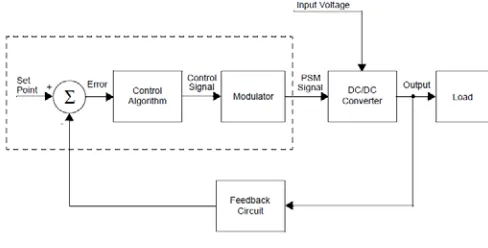
compares the output to a set point, performs a control algorithm and applies the output to a modulator which is used to drive the DC/DC Converter.
2.0 Operation of DC-DC Buck Converter
The buck converter shown in Figure 1.0 is
the main power management circuit of a DC/DC
Converter system using PIC16F88 to implement the controller function in a voltage-controlled
MPPT bus. The microcontroller is used to
generate the set-point, error amplification, control algorithm and modulation.
A sensing or feedback control circuit is usually needed to monitor the output voltage so that it can be maintained within the desired voltage level by switching frequency and or duty cycle variation. Therefore when the switch turns on, the current from the input source flows through the switch and inductor, and into the capacitor and the load resistor. During this period, the magnetic field in the inductor builds up the stored energy. When the switch is off, the inductor sustains current flow to the load for a part or the rest of the switching cycle. Literatures have widely acclaimed buck converters as good for charging lead-acid batteries [4-5]. The main advantage of these switching regulators are their high efficiency which entails smaller heat sinks to dissipate the heat [6-7]. In addition, the energy stored by inductor and capacitor can be transformed to output voltage.
Figure 1.0: The Circuit Diagram of a Buck Converter
2.1 Buck Converter in a Continuous Operation mode
The buck converter was designed to operate in the continuous operation mode which means the current through the inductor (L) does not drop to zero during the commutation cycle. This is shown in Figure 2.0.
Figure 2.0: The Signal Waveform of the Voltage and Current for a Buck Converter
When the switch is ON, then the inductor current will be
𝑖𝑖𝐿𝐿 =�𝑉𝑉𝑠𝑠𝐿𝐿−𝑉𝑉𝑜𝑜
𝑚𝑚 � 𝑡𝑡+𝐼𝐼1 1.0
And change in the inductor current during the ON period will be
𝛥𝛥𝑖𝑖𝐿𝐿 =�𝑉𝑉𝑠𝑠𝐿𝐿−𝑉𝑉𝑚𝑚𝑜𝑜� 𝐷𝐷𝑡𝑡 2.0
When the switch is OFF, the inductor current will be
𝑖𝑖𝐿𝐿 =−𝐿𝐿𝑉𝑉𝑚𝑚𝑜𝑜 (𝑡𝑡 − 𝐷𝐷𝐷𝐷) +𝐼𝐼2 ` 3.0
And change in inductor current during the OFF period will be
𝛥𝛥𝑖𝑖𝐿𝐿 =−𝐿𝐿𝑉𝑉𝑚𝑚𝑜𝑜 (1− 𝐷𝐷)𝐷𝐷 4.0
Substituting equation 2 in 4 will give the relationship
𝑉𝑉𝑜𝑜 =𝐷𝐷𝑉𝑉𝑠𝑠 5.0
For 0≤ 𝐷𝐷 ≤1
The critical inductance which is the minimum inductance that will ensure that the inductance current remains above zero throughout the cycle is
𝐿𝐿𝑀𝑀𝑀𝑀 =2𝑓𝑓𝑅𝑅 (1− 𝐷𝐷) 6.0
The input Power (Pin) is the sum of the
average power delivered to the load and the average total internal power consumption of a buck and output Power (Po) is the average power
delivered to the load can be used to compute the efficiency of the converter and it is as shown in equation 7.0. Where P is the average power
C1 R1
21 E1
L
D1
VS
+ vo
_
+ Vo
_ R C
International Journal of Scientific and Research Publications, Volume 9, Issue 9, September 2019 323 ISSN 2250-3153
delivered to the load and Pbuck is the average total
internal power consumption of a buck converter as given by
𝐸𝐸𝐸𝐸𝐸𝐸𝑖𝑖𝐸𝐸𝑖𝑖𝐸𝐸𝐸𝐸𝐸𝐸𝐸𝐸 (𝜂𝜂) = 𝑃𝑃𝐿𝐿𝑜𝑜𝐿𝐿𝐿𝐿
𝑃𝑃𝐿𝐿𝑜𝑜𝐿𝐿𝐿𝐿+𝑃𝑃𝑏𝑏𝑏𝑏𝑏𝑏𝑏𝑏× 100% 7.0
3.0 Hardware and Software Design of the Buck Converter
PV solar modules with model number MX60/12 was used for the prototype of the design and the block diagram of the system is as shown in Figure 3.0.
Figure 3.0: The Block Diagram of a Buck Converter Circuit
The system circuit design specifications for the Buck Converter are as follows:
S/n ITEM UNIT VALUE
1 Supply Voltage from PV
V 28≤ Vin
≥36
2 Voltage supplied to the battery (Vo)
V 28
3 Maximum power Watts 280 4 Output Ripple
Voltage
% 8
5 Output Ripple Current % 8
6 Duty cycle 0.81
7 Switching frequency kHz 2 8 Output current, A 10
Assuming 30% maximum ripple current (3A), VS = 33V, Vo = 28V and f = 2 kHz, then
the inductor will be L = 675 µH.
3.1 Feedback and Control Circuit Design
The power and driver circuits used are principally based on the working principle of IGBT driver EXB 841 which provides the required isolation for the power circuit. The integrated circuit has an inbuilt signal isolation circuit, driver amplifier, over-current detector, low speed over current cut-off circuit and gate turn-off power supply. The current sensor LA 55-P/SP1 which is a closed loop current transducer using hall-effect was used to measure the line current from output of the converter power circuit. It has a default turn ratio (Primary to Secondary) of 1:2000 and for a 10 A current measurement, the wire carrying the current was wound round the sensor 4 times which corresponds to a current of 12 mA. A resistor of 330 Ω was used to measure the equivalent voltage drop which corresponds to the current passing through the phase.
3.2 Design of the Software
The microcontroller used to generate the Pulse Width Modulation (PWM) signal is PIC16F88 which has necessary features to implement the DC-DC Buck Converter at fixed frequency and in continuous mode with minimal peripherals. It has an internal PWM and analogue input which measures the voltage level from the battery.
As the battery voltage increases, it reaches a pre-set threshold voltage of 28.0 V at which point the supply current begins to taper-off (only 5% duty cycle is supplied) to avoid the battery entering the overcharge state. A voltage divider is used to obtain the required maximum battery voltage of 28.0 V DC. VB is the Battery
voltage and it is equal to 28 V, while Vm is the analogue input to the microcontroller obtained from the voltage division by resistors R1 and R2.
The voltage division gives equation 8.0:
𝑉𝑉
𝑚𝑚=
𝑅𝑅𝑉𝑉𝐵𝐵.𝑅𝑅2 [image:3.612.56.300.263.387.2]International Journal of Scientific and Research Publications, Volume 9, Issue 9, September 2019 324 ISSN 2250-3153
The resistors R1 was chosen to be 6 kΩ while R2 was chosen to be 1 kΩ. To compute the scaling factor for a maximum duty cycle of 255 counts by the microcontroller, using the voltage divisor ratio of 1/7 and battery terminal voltage of 28.0 V, the analogue input voltage to the microcontroller from the voltage division Vm is 4
V.
Since PIC16F88 is an 8-bit microcontroller with reference of 5 V, therefore 28V battery terminal voltage will give an equivalent microcontroller count of 204 with a scaling factor of 7.29. For the 28.0 V maximum battery terminal voltage, the cut-off voltage to avoid over-charging the battery will be an equivalent digital count by the microcontroller less or equal to 204. For the battery to be protected from being depleted below the Depth of Discharge (DoD), the battery should not be depleted below 24 V which is equivalent to an analogue input of 3.43 V or digital count of 175. Therefore the microcontroller should count equal or greater than 175 only.
The algorithm for charging the battery was written to produce a charging current that is tapered to a preset current threshold (usually 0.2 × Bulk current), it switches to the float charge mode, in which the battery voltage is maintained at a constant level. Reaching the float charge mode also means that the battery is fully charged.
4.0 Results and Discussion
The logic algorithm for the control of the Buck converter were written in the Simulink interface in MATLAB version 7.7. While a laboratory prototype of the static switch control was implemented to compare the experimental signal waveforms with the simulations earlier made. The two key parameters of interest are the switching voltage and current which are required to charge the battery.
4.1 MATLAB Simulation of the Buck Converter Charger
The complete circuit diagram using Simulink Simulation package is as shown in Figure 6.0. The waveforms obtained from the simulation and configuration dialogue box are as given in Figures 4.0 – 6.0.
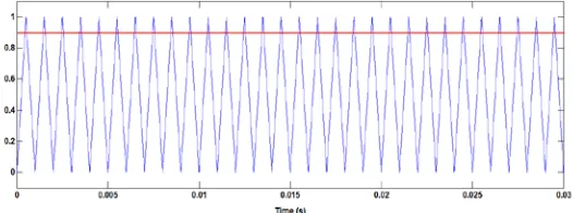
[image:4.612.330.593.357.455.2]Figure 4.0 shows the reference triangular wave of the DC-DC buck converter and the feedback from the battery voltage. Any slight difference between the feedback voltage and reference voltage results in a swing in the error output voltage and consequently the duty cycle. This error voltage controls (modulates) the pulse width of the output signal and is shown in Figure 5.0. It uses voltage feedback from the battery to avoid the battery going into deep discharge and overcharge.
[image:4.612.325.594.376.633.2]Figure 4.0: The Reference Triangular Wave Signal and Battery voltage Feedback Voltage.
Figure 5.0: The Pulse Width Modulation Signal for Charging the Battery.
International Journal of Scientific and Research Publications, Volume 9, Issue 9, September 2019 325 ISSN 2250-3153
[image:5.612.323.559.179.350.2]current for a battery at the start of recharge can be any va1ue that does not produce an average ce11 vo1tage in the battery string greater than the gassing voltage. High recharge rates are less efficient and that informed using 10 A for charging of the battery to reduce the battery and cabling losses due to over-heating. This low charging current is desirable to minimize overcharge, grid corrosion associated with overcharge and water loss by electrolysis of the electrolyte.
Figure 6.0: The Current Supplied from Switch to the Buck Converter Inductor
4.2 Experimental Setup for the Buck Converter
A buck converter was built using PIC16F88 microcontroller to generate the switching pulses at 2 kHz. The experimental setup shown in Figure 7.0 is the complete circuit of the Battery charge controller which cuts the charging current to the battery at 10 A.
Figure 7.0: Experimental Setup of the Buck Converter Battery Charger
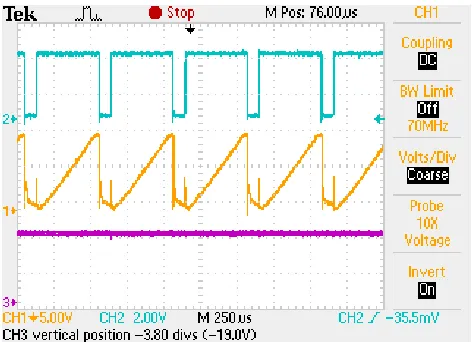
The waveforms of the buck converter circuit are as shown in Figures 8.0 and 9.0. The switching pulse is generated at frequency of 2 kHz and duty cycle of 81 % to drive the power circuit.
Figure 8.0: The Wave Shape of the PWM Signals, Charging Current and Load DC Voltage.
As shown in Figure 8.0, the charge current increases when the switching pulse is in the ON-state and decays when the switching pulse is in the OFF-state. The inductor introduced some spikes during switching period. As the voltage from the solar panel increases, the duty cycle decreases to maintain 28 V charging voltage across the battery. The output voltage increases as the ON-state pulse width increases.
[image:5.612.55.300.548.731.2]ISSN 2250-3153
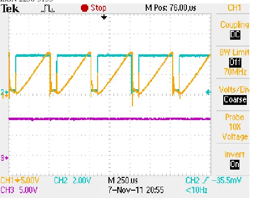
Figure 9.0: The Wave Shape of the Switching Pulses at 81.2% Duty-cycle superimposed on the Load Current.
The average efficiency of the static converter circuit was found to be 88.76% which means only an average of 11.24% of the power is lost due to conversion.
5.0 Conclusion
The control logic for the power electronic circuits is microcontroller-based which is aimed at reducing the components and improving the efficiency of the system. In the common solar refrigerators in the market, the charge controllers and compressors are made by different manufacturers.
The charging current for a battery at the start of recharge can be any va1ue that does not produce an average ce11 vo1tage in the battery string greater than the gassing voltage. High recharge rates are less efficient and that informed using 10 A for charging of the battery to reduce the battery and cabling losses due to over-heating. This low charging current is desirable to minimize overcharge, grid corrosion associated with overcharge and water loss by electrolysis of the electrolyte.
6.0 References
1. Goshwe, N. Y., Afiagh, T. and Igwue, G. A. (2013): Sizing and Cost Analysis of a Standalone Solar Photovoltaic Electric Generator for a Typical Small Commercial Bank in Nigeria. Proceedings of IEEE International Conference NIGERCON, November 14 – 16, 2013. Pg 242 – 246
2. Hartono Darmawaskita, 2002: DC/DC Converter Controller Using a PICmicro Microcontroller. Microchip Technology Inc, USA
3. M. Jantsch, M. Real, H. Haberlin, C. Whitaker, K. Kurokawa, G. Blasser, P. Kremer and C. G. Verhoeve (1998) “Measurement of PV Maximum Power Point Tracking Performance”, www.ecn.nl/docs/library/report/1997/rx9 7040.pdf, 1998.
4. G. R. Walker, “Evaluating MPPT converter topologies using a MATLAB PV model” Australasian Universities Power Engineering Conference, AUPEC 2000, Brisbane, 2000,
5. E. Koutroulis, K. Kalaitzakis, and C. V. Nicholas, “Development of a Microcontroller-Based Maximum Power Point Tracking Control System”, IEEE Transactions on Power Electronics, Vol. 16, N0 1, 2001.
6. H. J. Chiu, C. J. Yao Y. K. and Lo, “A DC/DC Converter Topology for Renewable Energy Systems”, International Journal of Circuit Theory and applications. Vol 37, Issue 3, 2009, pp 485-495.
[image:6.612.54.319.51.253.2]International Journal of Scientific and Research Publications, Volume 9, Issue 9, September 2019 327 ISSN 2250-3153
8. A. Prodic, D. Maksimovic and R. W. Erickson, “Design and Implementation of a Digital PWM Controller for a High-Frequency Switching DC-DC Power