Implementation of Low Power Parallel Compressor for
Multiplier using Self Resetting Logic
Suparshya Babu Sukhavasi,
Assistant professorDepartment of ECE K L UNIVERSITY
Susrutha Babu Sukhavasi
Assistant professorDepartment of ECE K L UNIVERSITY
ABSTRACT
In this paper a new approach of reducing power for a given system is developed that is self resetting logic, a parallel compressor is developed for multiplier by reducing its power with facilitation of this low power logic technique. By using this technique the power dissipation is significantly reduced with respect to other logics. By implementing the parallel compressor the performance of the circuit is increases.
Keywords
High speed, VLSI, Self-resetting logic (SRL), topologies, power dissipation
1.
INTRODUCTION
In today„s prompt processing environment, the use of dynamic circuits is becoming increasingly popular [5]. Dynamic CMOS circuits are defined as those circuits which have an additional clock signal inputs along with the default combinational circuit inputs of the static systems. Dynamic systems are faster and efficient than the static systems. A deep-seated difficulty with dynamic circuits is the monotonicity requirement. Addition is a fundamental arithmetic operation that is generally used in many VLSI systems, such as application-specific digital signal processing (DSP) architectures and microprocessors [2]. This module is the core of many arithmetic operations such as addition/subtraction, multiplication, division and address generation. Such high performance devices need low power and area efficient adder circuits. So this paper presents a design construction for primitive gates and adder circuits which reduce delay and clock skew when compared to the dynamic logic adder implementation [9].
After a logic gate has processed a set of input pulses, a reset signal is activated that restores the logic gate to a state in which it can receive another set of input pulses. The reset operation is timed to occur after the input pulses have returned to zero. Thus, there is no need for an evaluate or “foot” transistor since the pull-down network will be off during the reset operation, and this is one of the factors that leads to high-speed operation. Moreover, since the reset occurs immediately after each gate has evaluated, there is no need for a separate precharge phase. Since short-duration pulses are hard to debug and test, special additional test-mode features are sometimes added for these purposes. Two types of reset
structures have been proposed for use in SRCMOS. In globally self-resetting CMOS [4], the reset signal for each stage is generated by a separate timing chain which provides a parallel worst-case delay path. Individual reset signals are obtained at various tap points along this timing chain in such a way that the reset pulse arrives at each stage only after the stage has completed its evaluation.
Very careful device sizing based on extensive simulations over process-voltage-temperature corners are required in order to ensure correct operation. Moreover, any extra delay margin that is designed into the timing chain simply reduces the throughput by a corresponding amount. On the other hand, in locally self-resetting CMOS [5], the reset signal for each stage is generated by a mechanism local to that stage. Previous implementations of this technique have been based on single-rail domino stages in which the reset signal is obtained by sending the stage‟s own output signal through a short delay chain. Again, this technique requires very careful simulations and device sizing in order to ensure that the reset signals do not arrive too early. As with the other technique, any timing margin that is built in will directly limit the achievable performance.
2.
SELF
RESETTING
CMOS
DYNAMIC LOGIC
Self-resetting logic is a commonly used piece of circuitry that automatically precharge they (i.e., reset themselves) after a prescribed delay [3]. They find applications where a small percentage of gates switch in a cycle, such as memory decoder circuits. It is a form of logic in which the signal being propagated is buffered and used as the precharge or reset signal. By using a buffered form of the input, the input loading is kept almost as low as in normal dynamic logic while local generation of the reset assures that it is properly timed and only occurs when needed [6].
A generic view of a self-reset logic is shown in Fig.1. In the domino case, the clock is used to operate the circuit. In the self-resetting case, the output is fed back to the precharge control input and, after a specified time delay, the pull-up is reactivated. There is an NMOS sub block where the logic function performed by the gate is implemented which is represented as NMOS_LF through which the input data„s are loaded. The output of the gate F provides a pulse if the logic
Vijaya Bhaskar Madivada
M.Tech Student Department of ECEK L UNIVERSITY
S R Sastry Kalavakolanu
M.Tech StudentDepartment of ECE K L UNIVERSITY
Habibulla khan
Professor & Head
function becomes true. This output is buffered and it is connected to PMOS structure to precharge [7]. The delay line is implemented as a series of inverters. The signals that propagate through these circuits are pulses. Dynamic logic circuits are widely used in modern low power VLSI circuits. These dynamic circuits are becoming increasingly popular because of the speed advantage over static CMOS logic circuits; hence they are widely used today in high performance and low power circuits. Normally in the design of flip-flops and registers, the clock distribution grid and routing to dynamic gates presents a problem to CAD tools and introduces issues of delay and skew into the circuit design process [1]. There are situations that permit the use of circuits that can be automatically precharge themselves (i.e., reset themselves) after a prescribed delays [7]. These circuits are called post charge or self-resetting logic which are widely used in memory decoders. In this case, and charges to give an output voltage of this is fed through the triple-inverter chain to drive the gate voltage of MR to 0v after a delay of where is the delay through one inverter.
VDD VSGR Delay chain
MP MR
tp tp tp
CX VX COUT VOUT
inputs
Fig.1: Basic Structure of a Self Resetting Logic Circuit
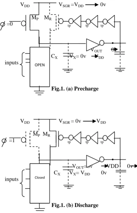
Self-resetting logic (SRL) can be classified as a variant of domino logic that allows for asynchronous operation. A basic SRL circuit is shown in Figure. A careful inspection of the schematic shows that the primary differences between this gate and the standard domino circuit are (a) the addition of the inverter chain that provides feedback from the output voltage Vout(t) to the gate of the reset pFET MR, and (b) the elimination of the evaluation nFET. Note that an odd number of inverters (3) are used in the feedback [7]. As discussed below, the feedback loop has a significant effect on both the internal operation of the circuit and the characteristics of the output voltage. Precharging of Cx occurs when the clock is at a value Ф=0 and the circuit conditions are shown in Figure (a). During this time, and which is identical to the event in a standard domino circuit. As we will see, the timing of the input signals precludes the possibility of a DC discharge path to ground by insuring that the inputs to all logic nFET are 0 during precharge.
The voltage on the gate of MR is at a value of so that insures that MR is in cutoff during this time. The distinct features of SRL arise when a discharge occurs. The circuit conditions are shown in Figure (b).
Since now we have that MR is active which allows to flow and recharge back up to a voltage of This action resets the output voltage to its original precharge value of giving the logic family its name: it automatically resets its output to 0.To
gain a better understanding of the voltage transitions involved in a self-resetting logic gate, let us analyze the circuit shown in figure which implements the AO function
VDD VSGR =VDD 0v
MP MR
=0 tp tp tp
VOUT 0v
CX VX= 0v VDD
inputs
Fig.1. (a) Precharge
VDD VSGR = 0v VDD
MP MR
=1 tp tp tp
VOUT=0v VDD 0v
CX VX= VDD 0v
inputs
Fig.1. (b) Discharge
3.
PARALLEL COMPRESSOR LOGIC
Compressors are habitually used in multipliers to trim down the operands while adding terms of partial products. A compressor Ci is a combinatorial device that compresses N
[image:2.595.308.528.128.468.2]input lines in the position i to 2 output lines i.e. sum and carry. In addition, there are L inputs lines coming to the compressor to different levels j. Figure shows a simple compressor.
Fig.2: A Generic Compressor
[3:2] Compressor
A [3:2] compressor is chiefly a Full adder. It has 3 inputs A, B and C to be summed up and provides 2 outputs (sum and carry). Gate level diagram of [3:2] compressor is shown in Figure .
GENERIC
COMPRESSOR
N
L
L
2
ClosednFET
logic
[image:2.595.49.257.296.440.2] [image:2.595.343.512.566.671.2]Fig.3: Gate level design of [3:2] compressor [4:2] Compressor
4 to 2 compressor is shown in figure 3. It takes 4 inputs of equal weight and produces two outputs. [4:2] compressor can be used in binary tree to produce a much more regular layout. It can be constructed from two [3:2] compressors and OR gate. Hence we see that it also plays an important role in optimizing the partial products. Talking about design of this compressor it consist of two 1-bit full adders placed in series, first full adder takes in the three inputs to be added and the next full adder takes in the fourth bit to be added, sum of the first adder and third input is grounded.
[image:3.595.52.278.388.531.2]Fig.4: [4:2] Compressor using [3:2] compressors
Table.1. Truth table for [4:2] Compressor
INPUTS OUT PUTS
A B C C1 SUM CARRY
0 0 0 0 0 0
0 0 0 1 1 0
0 0 1 0 1 0
0 1 0 0 1 0
1 0 0 0 1 0
0 0 1 1 0 0
0 1 0 1 0 1
0 1 1 0 0 1
1 0 0 1 0 1
1 0 1 0 0 1
1 1 0 0 0 1
0 1 1 1 1 1
1 0 1 1 1 1
1 1 0 1 1 1
1 1 1 0 1 1
1 1 1 1 0 1
The carryout of first adder and the second adder is given as input to OR Gate. Output of the OR Gate is the carryout of the [4:2] compressor and the output of the second full adder is the sum of the [4:2] compressor. Block diagram of [4:2] compressor is shown above. This results in seven partial products at second level which are reduced to three and from then to two using arrays of full adders (i.e., (3:2) counters) [9]. If this modified approach were not used, there would have been eight partial products at the second level and four at the next level. The (4:2) compression would have been required at the third level which would have added to the delay and the gate count. Half-adders (2,2), full adders (3,2), (4,3) counters or (4:2) compressors, (5,3) counters or (5:3) compressors, and (6,3) counters or (6:3) compressors were used at the right and left end of the top two levels. (4,3), (5.3) and (6,3) counters are modified (7.3) counters with slightly reduced gate count. Similarly, (5:3) and (6:3) compressors are modified (7:3) compressors. The partial product matrix is generated using an array of AND gates. In the Wallace multiplication scheme, each row of the partial product matrix is input to an array of adders (compressors). Asshown in Figures, this was modified slightly to reduce the overall delay. Thus, partial products included in the first block are the ones in the top seven rows plus some of the bit products from the two rows below. This is shown by the solid line which steps down on the left [11]. The same procedure is repeated for the second block at the top level. As a result of this modification, four bit products are left at the lower right comer (columns 14, 15 and 16) of the partial product matrix. These are reduced to one partial product using two half adders. This results in seven partial products at second level which are reduced to three and from then to two using arrays of full adders (i.e., (3:2) counters).
[image:3.595.314.545.395.738.2]4.
IMPLEMENTATION OF SRL IN
PARALLEL COMPRESSOR
Fig.5: full adder using self resetting logic
Fig.6: full adder schematic result using self resetting logic
A
C
SUM
CARRY B
Cin
SUM
C A R R Y
FA
FA
O
R
A [image:3.595.47.283.553.765.2]Fig.7: [4:2] parallel compressor using two [3:2] compressors designed by self resetting logic
Fig.8: schematic results of [4:2] parallel compressor using two [3:2] compressors designed by self resetting logic
[image:4.595.53.288.72.484.2]Fig.9: half adder using self resetting logic
[image:4.595.315.543.80.277.2]Fig.10: schematic results of half adder using self resetting logic
Fig.11: Schematic of 4 x 4 multiplier using self resetting logic designed with parallel compressor
[image:4.595.313.552.251.721.2] [image:4.595.55.281.508.720.2]Fig.13: Results of 4 X 4 Multiplier
[image:5.595.331.540.110.253.2]5.
COMPARISON BETWEEN SRL AND
DYNAMIC LOGIC CIRCUIT
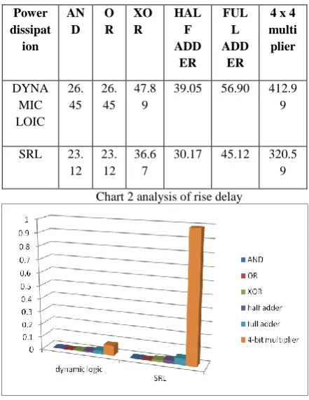
Table.2. Power Dissipation in self resetting logic
Topology Rise delay
Ns
Fall delay
ns
Power
Dissipation(mW)
AND 0.005 0.001 23.12
OR 0.004 0.001 23.12
XOR 0.015 0.002 36.67
HALF ADDER
0.024 0.022 30.17
FULL ADDER
0.050 0.043 45.12
4 x 4 multiplier
[image:5.595.318.539.296.582.2]0.990 0.801 320.59
Table.3. Power Dissipation in dynamic logic
Topology Rise delay
Ns
Fall delay
ns
Power
Dissipation (mW)
AND 0.003 0.005 24.21
OR 0.002 0.005 24.21
XOR 0.005 0.004 43.35
HALF ADDER
0.012 0.033 35.19
FULL ADDER
0.025 0.014 50.21
4 x 4 multiplier
0.0780 0.669 412.99
Chart 1: analysis of power dissipation
Table.4. Comparative Analysis of Power Dissipation
Power dissipat ion
AN D
O R
XO R
HAL F ADD
ER
FUL L ADD
ER
4 x 4 multi plier
DYNA MIC LOIC
26. 45
26. 45
47.8 9
39.05 56.90 412.9 9
SRL 23. 12
23. 12
36.6 7
30.17 45.12 320.5 9
Chart 2 analysis of rise delay
6.
CONCLUSION
[image:5.595.40.285.561.757.2]7.
REFERENCES
[1] Woo Jin Kim, Yong-Bin Kim, ―A Localized Self-Resetting Gate Design Methodology for Low Power‖ IEEE 2001.
[2] M. E. Litvin and S. Mourad, ―Self-reset logic for fast arithmetic applications,‖ IEEE Transactions on Very Large Scale Integration Systems, vol. 13, no. 4, pp. 462– 475, 2005.
[3] L. Wentai, C. T. Gray, D. Fan, W. J. Farlow, T. A. Hughes, and R. K. Cavin, ―250-MHz wave pipelined adder in 2-μm CMOS,‖ IEEE Journal of Solid-State Circuits, vol. 29, no. 9, pp. 1117–1128, 1994.
[4] D. Patel, P. G. Parate, P. S. Patil, and S. Subbaraman, ―ASIC implementation of 1-bit full adder,‖ in Proc. 1st Int. Conf. Emerging TrendsEng. Technol., Jul. 2008, pp. 463–467.
[5] M. Lehman and N. Burla, ―Skip techniques for high-speed carry Propagation in binary arithmetic units,‖ IRE Trans. Electron.comput., vol. EC-10, pp. 691–698, Dec. 1962.
[6] R. A. Haring, M.S. Milshtein, T.I. Chappell, S. H. Dong and B.A. Chapell, "Self resseting logic and incrementer" in Proc. IEEE Int. Symp. VLSI Circuits, 1996 pp. 18-19.
[7] G. Yee and C. Sechen, " Clock-delayed domino for adder and combinational logic design" in proc.IEEE/ACM Int. Conf. Computer Design, Oct., 1996, pp. 332-337.
[8] P. Ng, P. T. Balsara, and D. Steiss, ―Performance of CMOS Differential Circuits,‖ IEEE J. of Solid-State Circuits, vol. 31, no. 6, pp. 841-846, June 1996.
[9] P. Srivastava, A. Pua, and L. Welch, .Issues in the Design of Domino Logic Circuits, Proceedings of the IEEE Great Lakes Symposium on VLSI, pp. 108-112, February 1998.
[10]W. Zhao and Y. Cao. ―New generation of predictive technology model for sub-45nm design exploration,‖ In IEEE Intl. Symp. On Quality Electronics Design, 2006
![Fig.3: Gate level design of [3:2] compressor [4:2] Compressor](https://thumb-us.123doks.com/thumbv2/123dok_us/8112375.791436/3.595.60.285.75.285/fig-gate-level-design-compressor-compressor.webp)
![Fig.8: schematic results of [4:2] parallel compressor using two [3:2] compressors designed by self resetting logic](https://thumb-us.123doks.com/thumbv2/123dok_us/8112375.791436/4.595.53.288.72.484/schematic-results-parallel-compressor-using-compressors-designed-resetting.webp)