Network on Chip for 3D Mesh Structure with Enhanced
Security Algorithm in HDL Environment
Adesh Kumar
Assistant Professor, Department of Electronics Engineering,
University of Petroleum & Energy Studies, Dehradun,
India
Sonal Singhal,
PhD. Assistant Professor, Departmentof Electrical Engineering, Shiv Nadar University, Gautam Buddh Nagar, NCR, India
Piyush Kuchhal,
PhD. Associate Professor & Head,Department of Physics, University of Petroleum & Energy Studies, Dehradun,
India
ABSTRACT
Network on chip (NOC) architecture is an approach to develop large and complex systems on a single chip. In this work 3D mesh topological structures has been implemented with enhanced TACIT Security in HDL environment. The architecture supports physical and architectural level design integration. Basic communication mechanism between resources is envisioned to be packet switched message passing through the switches. For the node identification in 3D networks 8 × 8 × 8 Mesh configuration is taken. A new Algorithm is proposed for secured data transmission among nodes. TACIT algorithm is used for data encryption and decryption and applicable for n bit block size and key. Design is implemented in Xilinx 14.2 VHDL software, and functional simulation was carried out in Modelsim 10.1 b, student edition. Hardware parameters such as size cost and timings are extracted from the design code.
General Terms
TACIT Security, Simulation, Synthesis, Integrated Circuits, Intellectual Property
Keywords
Very High Speed Integrated Circuit hardware Description language (VHDL), Network on chip (NOC), System on chip (SOC)
1.
INTRODUCTION
Today, many integrated circuits contain several processor cores, memories, hardware cores and analog components on the same chip [3]. Such Systems on Chip (SoC) are widely used in high volume and high-end applications, such as multimedia, aerospace and defense, wired and wireless communication systems. With the scaling in IC technology more and more processors are integrating on a single die and formed a multiprocessor system on chip (MPSoC). It results in the increase in the power consumption and wire delay [22]. In addition to this, with increased number of transistors and the die size, length of the interconnects also increases. With reducing geometries, the wire pitch and cross section also reduces, thereby increasing the RC delay of the wires [22]. This coupled with increasing interconnect length leads to long timing delays on global wires. Another major impact of increased lengths and RC values is that the power consumption of global interconnects become significant, thereby posing a big challenge for system designers. Current on-chip interconnects [18] consist of low-cost shared communication resources, where arbitration logic is needed for the serialization of bus access requests: only one master at a time can drive the bus. Major drawback of this solution is its lack of scalability, which will result in unacceptable performance degradation (e.g,
contention-related delays for bus accesses) when the level of SOC integration will exceed a dozen of cores. Moreover, the connection of new blocks to a shared bus increases its associated load capacitance, resulting in more energy consuming bus transactions. Such factors make the on-chip communication among cores difficult. Therefore a scalable, energy-efficient on-chip interconnect network is needed to address these difficulties in order to expedite the on-chip communication [3].
principles for design of routers for NOC [10]. Routing protocol for Mesh Topological Structure is implemented, Different Switching techniques, such as circuit switching, packet switching is implemented. NOC architecture [10][25] follows the bus based architecture, bus implementation is done for NOC, and for example AMBA bus for ARM Processor, Peripheral Controller interface (PCI) bus which connects the hardware to PC.
This work carries out the implementation of the chip for 3D 8 x 8 x 8 Mesh Topological structures with secured data transmission among nodes. It employs the cross bar structure. Traffic can be diverted to any node by their address. Time division multiplexing techniques is used to detect the node which is applicable in telecommunication switching.
Tools Utilized: Design and implementation includes the ISE Design Suit 14.2, Xilinx software. It is used to design the IC and to view their RTL (Register Transfer Logic) schematic. ModelSim EE 10.1b students edition, Mentor Graphics is used for simulation and debugging the functionality. The chip implementation is done using VHDL programming language.
The paper is organized as follows: Section I presents the introduction and the tools utilized. Section II discusses the TACIT Security Algorithm. Section III presents the 3D mesh network. Section IV describes the Result and Performance Evaluation. Conclusion is presented in Section V.
2.
TACIT SECURITY ALGORITHM
There are many encryption and decryption algorithms which are already proposed. A comparison [2] of all is shown in table 1 listed below. Table 1 list the comparison of various encryption algorithms on the basis of Type and Features. It can be seen that from this comparison table that TACIT Encryption Technique has a unique independent approach by using some suitable mathematical logic along with a new key distribution system which is being applied on a secure policy based routing [8]. The main advantage of TACIT logic is that it can processes n-bit blocks and n- bit key size. This approach may be good if the block size is less than the key size [2] [23]. The algorithm may be implemented in all the languages support Unicode system facility like Java, C#, .Net, etc.
Table 1 Comparison of various encryption algorithms [21] on the basis of Key size and Block size.
Algorithm Key size(Bits)
Block size(Bits)
Features
DES 64 64 Most common, Not
strong enough Triple
DES
192 64 Modification of DES, Adequate security AES Variable
(192 or 256)
128 Replacement of DES, Excellent security, limited key size Kasumi
Encryption core
128 64 Designed for Third Generation
Partnership
Project(3GPP), used in Universal Mobile Telecommunication System UMTS, limited to 64-bit word size
Blowfish 448 64 Excellent security, No. of bits are variable ranging from 16-448 bits.
RSA 1024 128 Asymmetric
algorithm, speed is low
RC4 Variable(4 0 or 128)
Variable (32,64,12 8)
Fast stream chipper in Secured Socket Layer (SSL), more memory is required since they work on large chunk of data (stream) instead of block cipher.
X-MODES
32 32 Enhanced security
level & faster. TACIT
Encryption n-bit (ncan vary)
n-bit Good for small size of packets
2.1 Data Encryption Logic for TACIT
Algorithm
To implement the TACIT Logic [2] [23] for data communication between two nodes of NOC the following algorithm has been used. The corresponding VHDL coding has been developed and results are presented in section IV. Step 1: Text file content is read and position of the character is shuffled by using initial permutation approach using key value. Step 2: Read the character from the text file corresponding to the text and get the ASCII value of that character.
Step 3: Perform XOR operation with the specific n-bit key value.
Step 4: A secure tacit logic has been introduced (i.e. nk xor kk along with some specific operations; where n is the value computed from step 3).
Step 5: Convert the value into binary one.
Step 6: Perform reverse operation on the binary string. Step 7: Corresponding decimal value is found.
Step 8: The Unicode character corresponds to the decimal value is formed which is none other than the cipher text. Step 9: Continue step 1 to 7 for the next characters of the file until End of File (EOF) is reached.
2.2
Data Decryption Logic for TACIT
Algorithm
The decryption algorithm [23] at the receiving end follows the following steps. In the decryption logic user can share the same key.
Step 1: Read the first character from the cipher text and get the corresponding decimal value of it.
Step 2: The corresponding binary value is evaluated and make the reverse of it.
Step 3: Inverse of the tacit logic is applied. Step 4: Perform XOR with n-bit key value.
Step 5: The character corresponds to it is determined. Step 6: Now reshuffling is done using key value. Step 7: Repeat the steps (1 to 6) till the end.
3.
3D MESH NETWORK
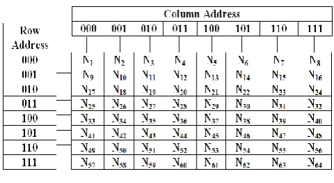
[image:2.595.310.556.72.230.2]considered in this work. With switching mesh network 64 nodes can be addressed at one time. And to address the 64 nodes 3 bits were required individually for both the axes (2n = 8). 3 bits row address is assigned to nodes on X axis. Similarly 3 bit address is assigned on the nodes on Y axis. Addressing and node selection scheme is described in the functional table (Table 2). It is evident from Table 2 that if the row address is 000 and column address is 110, node N6 is selected; similarly any node could be selected based on node address table having row address and column address. Figure 1 shows the cross point structure and the node locations on the X and Y axis.
[image:3.595.48.281.372.687.2]Figure 1, 2D Network structure (8 x 8)
Table 2 Node address generation scheme in 2D structure
Row Address Column Address Destination Node
000 000 Node 1
000 001 Node 2
000 010 Node 3
000 011 Node 4
000 100 Node 5
000 101 Node 6
000 110 Node 7
000 111 Node 8
001 000 Node 9
001 001 Node 10
001 010 Node 11
001 011 Node 12
001 100 Node 13
001 101 Node 14
001 110 Node 15
001 111 Node 16
010 000 Node 17
010 001 Node 18
010 010 Node 19
010 011 Node 20
010 100 Node 21
010 101 Node 22
010 110 Node 23
010 111 Node 24
011 000 Node 25
011 001 Node 26
011 010 Node 27
011 011 Node 28
011 100 Node 29
011 101 Node 30
011 110 Node 31
011 111 Node 32
100 000 Node 33
100 001 Node 34
100 010 Node 35
100 011 Node 36
100 100 Node 37
100 101 Node 38
100 110 Node 39
100 111 Node 40
101 000 Node 41
101 001 Node 42
101 010 Node 43
101 011 Node 44
101 100 Node 45
101 101 Node 46
101 110 Node 47
101 111 Node 48
110 000 Node 49
110 001 Node 50
110 010 Node 51
110 011 Node 52
110 100 Node 53
110 101 Node 54
110 110 Node 55
110 111 Node 56
111 000 Node 57
111 001 Node 58
111 010 Node 59
111 011 Node 60
111 100 Node 61
111 101 Node 62
111 110 Node 63
111 111 Node 64
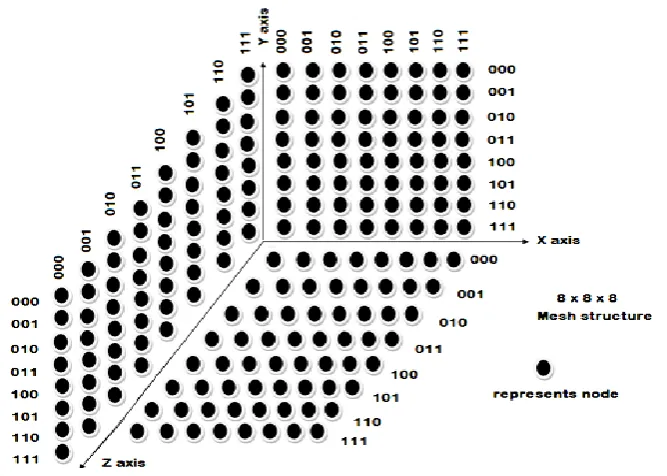
Figure 2 Three dimensional (3D) network structure for (8 x 8 x 8) switching cross point
Table 3 Node address generation scheme in 3D network structure
For example realization of the hardware of any NOC architecture is by the sequential statement in HDL, it takes the individual multiplexer for each logic realization, but if the same algorithm is realized by Parallel Processing [9] [22] [25] like using CASE statement or using Finite State machines (FSM), it takes only one multiplexer to realize all the logics. Therefore efficient coding is required to reduce the hardware, delay and power. For the chip implementation of 3D NOC, it was not possible to configure for all nodes at one time. Therefore network was divided into in 2D NOC in XY direction, 2D NOC in YZ, 2D NOC in ZX direction. The 2D NOC configuration in XY direction were assigned 3 bits for row addresses on X axis and 3 bits for column address on Y axis. The 2D NOC configuration in YZ direction were assigned 3 bits for column addresses on Y axis and 3 bits for third address on Z axis The 2D NOC configuration in XZ direction were assigned 3 bits for row addresses on X axis and 3 bits for third address on Z axis. The address generation scheme of 3D NOC is shown in the table 3.
As a specific example, let the node no. 64 needs to be identified. The node detection will only be realized the address in XY direction (X = Row address (110), Y = Column address (100)), YZ direction (Y = Column address (110), Z = Third address (100)) and ZX direction (Z = Row address (110), X = Third address (100)) will be transmitted.
4.
RESULT
&
PERFORMANCE
EVALUATON
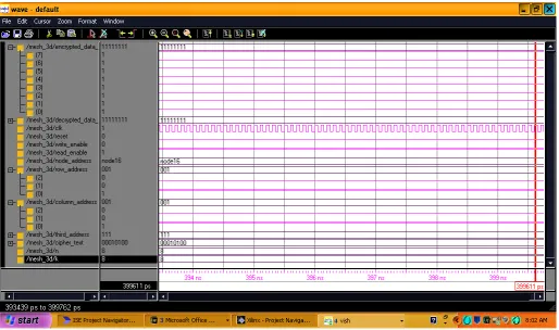
[image:5.595.314.553.375.504.2]The functional simulation of the 3D NOC structure is done with the help of Modelsim 10.1 b software and all the cases are tested. The snap shot for the same is shown in the figure 4. The design parameters of 3D NOC are listed in table 4.
Table 4 Design parameters and their functional description
Parameter Functional Description
reset used for synchronization of the components by using clk Clk To generate to clk pulse Node_address [4:0] address of destination node row_address [2:0] represents the address of the
nodes in x direction
column_address [2:0] represents the address of the nodes in y direction.
Third_address[2:0] represents the address of the nodes in z direction.
read_en control signals (read operation) write_en control signals (write operation) encrypted_data_in[7:0] represents input data of 8 bits decrypted_data_out[7:0] presents the output data of 8 bits
for the destination node.
cipher_text [7:0] presents the output data of 8 bits after encryption and input to decryption logic.
n data width of data, block size, integer
k Key size integer type
4.1 Simulation Process sequence
Step 1: reset = 1, clk is used for synchronization and then run. Step 2: reset = 0, same clk was used for synchronization. Step 3: Select the address of destination node Node_address. Step 4: Force the value of row_address and column_address of destination node.
Step 5: Select the value of block size n and key size k
Step 6: Give the eight bit value of data_in. Force write_en =1 and read_en =0 and then run.
Step76: write_en =0 and read_en =1 and run.Desired output on destination is achieved.
When write_en =1 and read_en =0, the data is written in temp variables of TACIT logics from the source node in encryption algorithm, when write_en =0 and read_en =1, the data is read from the temp variable of TACIT logics to destination node in decryption logic. Clk is applied at the positive edge clock pulse and reset is kept at 1 for the initial state, When reset = 0 the data is transmitted by encrypted_data_in [7:0]. The data length encrypted_data_in [7:0] and key size k is not constant, it can vary according to the requirement and application.
Figure 4 shows the simulated result for 8 x 8 x 8 3D NoC architecture. The coding for the implementation is done is the VHDL. The design parameters are similar to the 2D design with additional parameter for third address. Third address [2:0] represents the address of the nodes in z direction.
4.2 Device Utilization for 3D NOC
Device utilization report gives the percentage utilization [13] of device hardware for the chip implementation. Device hardware includes, logic gates, buffers, multiplexer, decoders, latches, flip flops etc. Register transfer Logic (RTL) is shown in the figure 3. Synthesis report shows the complete details of device utilization.
Figure 3 Xilinx RTL view of 3D NOC with TACIT Logic
Selected Device: xc3s50-5-tq144, this device is targeted for FPGA
Table 5 Device utilization in 3D structure
Device part Utilization
Number of Slices
Number of Slice Flip Flops Number of 4 input LUTs Number of bonded IOBs Number of GCLKs
10 out of 768 1% 16 out of 1536 1% 18 out of 1536 1% 25 out of 97 25% 2 out of 8 25%
4.3 Timing Summary
Timing [13] details provides the information of delay, minimum period, minimum input arrival time before clock and maximum output required time after clock
Speed Grade: -5
Minimum period: 2.010ns (Maximum Frequency: 497.401MHz)
[image:5.595.54.292.450.694.2]Figure 4 Modelsim output of 3D Mesh Topological Structure (8 x 8 x 8)
5.
CONCLUSION
Hardware implementation of the 3D topological mesh topology was carried out with TACIT Encryption and decryption algorithm. The major advantage of the programmable structure is to identify and replacement of the faulty node. In the network structure, stored program techniques are used. If the implementation of the entire structure is done by programmable switches and ICs, then the complexity of the system is reduced. Reprogramming NOC helps to identity the faulty node in the network structure. 3D NoC architecture was found more efficient for long data transfer. Since the signal can get any axis XY, YZ or ZX. There are very rare chances of signal being lost. 2D NoC architecture was found suitable for small area communication or LAN network but not in large area network. In the continuation of this work, a study can be carried out by taking into account the larger number of nodes.
6. REFERENCES
[1] W. Wolf, The future of multiprocessor systems-on-chips, in: Proceedings of the 41st Design Automation Conference (DAC’04), June2004, pp. 681–685.
[2] Manmeet Kaur, Manjit Kaur,Gurmohan Singh, C-DAC Mohali India, Comparison of TACIT Encryption Algorithm with Various Encryption Algorithms, International Journal of Electronics and Computer Science Engineering, page (1-10)
[3] Jason Cong, Yuhui Huang, and Bo Yuan Computer Science Department University of California, Los Angeles Los Angeles, USA, 978-1-4577-1400-9/11/$26.00 ©2011 IEEE, A Tree-Based Topology Synthesis for On-Chip Network ,pp 2-6
[4] Naveen Chaudhary, Bursty Communication Performance Analysis of Network-on-Chip with Diverse Traffic Permutations International Journal of Soft Computing and Engineering (IJSCE) ISSN: 2231-2307, Volume-1, Issue-6, January 2012, (page 1)
[5] Mohammad Ayoub Khan, Abdul Quaiyum Ansari, A Quadrant-XYZ Routing Algorithm for 3-D Asymmetric Torus Network-on-Chip, The Research Bulletin of Jordan ACM, ISSN: 2078-7952, Volume II (II) pp(18-26) [6] L. Benini, G. De Micheli, Networks on chip: a new SoC
paradigm, IEEE Comput. 35(1) (2002) 70–78.
[7] W. J. Dally, B. Towles, Route packets not wires: on-chip interconnection networks, in: Proceedings of Design Automation Conference (DAC’01), ACM, IEEE Press, New York, June 2001, pp. 648–689.
[8] F. Angiolini, P. Meloni, S. Carta, L. Benini, L.Raffo, Contrasting a NoC and a traditional interconnect fabric with layout awareness, in: Proceedings of Design, Automation and Test in Europe Conference and Exhibition (DATE’06), Munich, Germany, ACM, IEEE Press, NewYork, 2006,pp.124–129.
[9] Adesh Kumar, Arpit Jain, Rajeev Kumar, SMART Conference Proceedings, “Network On Chip Implementation Of 2D Mesh Topological Structure In HDL Environment , (page 1-6)
Stockholm, Sweden VTT Electronics, Box 1100, Oulu, FIN-90571, Finland
[11] S. Borkar, \design challenges of technology scaling." IEEE Micro, no.4, p. 2329, July-August 1999.
[12] Xin Wang and Jari Nurmi,Comparison of a Ring On-Chip
Network and a Code-Division Multiple-Access On-Chip Network, Hindawi Publishing Corporation VLSI Design Volume2007,ArticleID 18372, 14 page
[13] Semiconductor Complex Limited, Internet PDF: Data sheets of XC 95 series CPLD [Online]. Available: http://sclindia.com,
[14] K. Asanovi, R. Bodik, B. Catanzaro, J. Gebis, P. Husbands, K. Keutzer, D .Patterson, W. Plishker, J. Shalf, S. Williams, and K. Yelick, \The landscape of parallel computing research : A view from berkeley," University of California at Berkeley, December 2006. [Online]. Available: http: // parlab. eecs. berkeley. edu/ pubs/ EECS- 2006-183 .pdf
[15] S. Borkar, \design challenges of technology scaling." IEEE Micro, no.4, p. 2329, July-August 1999.
[16] Vitorde Paulo and Cristinel Ababei, 3D Network-on Chip Architectures Using Homogeneous Meshes and Heterogeneous Floorplans, Hindawi Publishing Corporation International Journal of Reconfigurable Computing Volume 2010, Article ID603059, 12 pages [17] M.Coppola, S.Curaba, M.Grammatikakis, R.Locatelli,
G.Maruccia, F.Papariello, L.Pieralisi, White paper on OCCN: A Network-On-Chip Modeling and Simulation Framework, ISD Integrated system developments, page 8
[18] Davide Bertozzi and Luca Benini, A Network-on-Chip Architecture for Gigascale Systems-on-Chip, IEEE Circuits and systems magazine, second quarter 2004, Xpipes, page (2-6)
[19] J. D. Owens, W. J. Dally etal., “Research challenges for on-chip inter connection networks,” IEEE MICRO, vol.27, no.5, pp.96–108,Oct.2007.
[20] A. Jantschand H.Tenhunen, Networks on chip. Kluwer Academic publishers, 2003
[21] T .Bjerregaard and S .Mahadevan,“A survey of research and practices of network-on-chip,” ACM Comp. Surveys, vol.38, no.1,pp.1–51,Mar.2006.
[22] Rikard Thid Thesis on “A Network on Chip Simulator”, Sweden Master of Science Thesis in Electronic System Design, Royal Institute of Technology Aug 2002, Page (9-27)
[23] Prosanta Gope, Ajit Singh, Nikhil Pawha, Ashwani Sharma, An Efficient Cryptographic Approach for Secure Policy Based Routing (TACIT Encryption Technique), 978-1-4244-8679-3/11/©2011 IEEE Page (1-4)
[24] Wen-Chung Tsai,, Ying- Cherng Lan,, Yu-Hen Hu, and Sao-Jie Chen Review Article “ Networks on Chips : Structure and Design Methodologies” Hindawi Publishing Corporation Journal of Electrical and Computer Engineering Volume 2012, Article ID 509465, 15 page [25] P. Pratim Pande, C. Grecu, M. Jones, A. Ivanov, and R.
![Table 1 Comparison of various encryption algorithms [21] on the basis of Key size and Block size](https://thumb-us.123doks.com/thumbv2/123dok_us/8096362.786295/2.595.310.556.72.230/table-comparison-various-encryption-algorithms-basis-key-block.webp)