Published Online October 2014 in SciRes. http://www.scirp.org/journal/jcpt http://dx.doi.org/10.4236/jcpt.2014.44024
How to cite this paper: Aono, M., Ueda, T., Abe, H., Kobayashi, S. and Inaba, K. (2014) Au Nanoparticle Formation from
Au Nanoparticle Formation from
Amorphous Au/Si Multilayer
Masami Aono1, Takashi Ueda1, Hiroshi Abe1*, Shintaro Kobayashi2, Katsuhiko Inaba2
1Department of Materials Science and Engineering, National Defense Academy, Yokosuka, Japan 2Application Laboratory, Rigaku Co., Akishima, Tokyo, Japan
Email: *[email protected]
Received 17July 2014; revised 17August 2014; accepted 16September 2014
Copyright © 2014 by authors and Scientific Research Publishing Inc.
This work is licensed under the Creative Commons Attribution International License (CC BY). http://creativecommons.org/licenses/by/4.0/
Abstract
By direct observations of transmission electron microscopy (TEM), irreversible morphological transformations of as-deposited amorphous Au/Si multilayer (a-Au/a-Si) were observed on heat-ing. The well arrayed sequence of the multilayer changed to zigzag layered structure at 478 K (=Tzig). Finally, the zigzag structure transformed to Au nanoparticles at 508 K. The distribution of
the Au nanoparticles was random within the thin film. In situ X-ray diffraction during heating can clarify partial crystallization Si (c-Si) in the multilayer at 450 K (=TML
MIC), which corresponds to metal induced crystallization (MIC) from amorphous Si (a-Si) accompanying by Au diffusion. On further heating, a-Au started to crystallize at around 480 K (=Tc) and gradually grew up to 3.2 nm
in radius, although the volume of c-Si was almost constant. Continuous heating caused crystal Au (c-Au) melting into liquid AuSi (ℓ-AuSi) at 600 K (=TmNP), which was lower than bulk eutectic tem-perature (TEB= 636 5 K± ). Due to the AuSi eutectic effect, reversible phase transition between liq-uid and solid occurred once temperature is larger than TmNP. Proportionally to the maximum tem- peratures at each cycles (673, 873 and 1073 K), both TmNP and Au crystallization temperature approaches to TEB. Using a thermodynamic theory of the nanoparticle formation in the eutectic system, the relationship between TmNP and the nanoparticle size is explained.
Keywords
Amorphous Au/Si Multilayer, Au Nanoparticle, Low Eutectic Point, Metal Induced Crystallization, Irreversible Morphological Transformation, Reversible ℓ-AuSi-c-Au Nanoparticle Phase
Transition
M. Aono .
1. Introduction
In metal silicides, metal-induced crystallization (MIC) [1]-[5] in thin films is well known to be a fundamental phenomenon relating to low eutectic point. Rather than viewing this phenomenon from a solid-phase reaction perspective, studies from the diffusion process view point are necessary due to the fact that electric screening weakens the covalent bonds of the amorphous Si (a-Si). Diffusion process in amorphous is a key to interpret the various phenomena in Au-Si system and apply it into a novel process for further functional materials.
The MIC process is classified into two groups: 1) eutectic alloy formation and 2) metallic compound assisted process. The former suggests that metal diffusion into a-Si is the main reason of MIC determined from the for-mation process of eutectics. By in situ observation of microstructure using electron microscopy [6], it was found that Au particles appear on the surface of a-Si at 573 K. Diffuse zone was also found between crystalline Au (c-Au) particles and the surrounding a-Si. Moreover, diffusion of Au into Si substrates was examined by X-ray reflectivity [7]. Surface sensitive diffusion is separated into Fickian-/non-Fickian-type, which is directly related to the surface stability. The latter described in 2) is characterized by a variety of crystal structures of the AuSi particles, which are induced in hydrogenated amorphous Si (a-Si:H) [8] and c-Au/a-Si thin film [9]. The me-tastable Au-silicides (Au2Si [10], Au5Si2, Au7Si, and so on) decomposed at higher temperature.
The surface nucleation on the substrate was investigated with respect to the eutectic phenomenon of Au1−xSix
[11]-[13]. A significant fact about the super cooling of c-Au nanoparticles on the Si (111) surface has been clari-fied by in situ observation of X-ray scattering and ab initio molecular dynamics [13]. It is understood that a nano- eutectic phenomenon is that the crystal nucleation is suppressed by a lateral order at interface. In the simulation box, a pentagonal cluster appears to be reconstructed on the interface.
Relating to crystal nucleation, irreversible morphological transformation occurred by the self-assembled me- chanism [14]. The mono disperse Au nanoparticles were obtained by thermal decomposition of the multilayer films. a-Au25Si75/a-Si multilayer was deposited on c-Si substrate. The stacking sequence is a-Si/a-Au25Si75/a-
Si/a-Au25Si75/a-Si/… with varying the a-Au25Si75 thickness as 10, 25, 50 and 100 nm, where the a-Si thickness is
fixed at 100 nm. As a different morphology in mono layer, spiral patterns of Au nanoparticles were formed in addition to the conventional dendritic phases [15]. The geometric array was generated in one Au1−xSix thin film
on Si substrate, whose thickness is 25 nm. On the other hand, cyclic 4.2 nm a-Si and 0.8 nm a-Au multilayer showed different irreversible transformations such as nanoparticles after annealing [16]. The thin film consists of 60 layers. Both the as-deposited and annealed samples were investigated in transmission electron microscope (TEM) observations, X-ray diffraction (XRD) and Raman scattering spectroscopy. The randomly located Au nanoparticle was observed after annealing. Also, the morphological changes were seen in Au/Ge multilayer, known as low eutectic point [17]. The size of c-Au particles increases with increasing Au layer thickness.
For industrial applications, nano-processing using binary eutectic alloys is utilized widely in a various kinds of scientific fields. For instance, well-arrayed Au nanoparticle enables control of coherent localized optical fields, which can be applied to chemical and biological sensors [18]. Surface plasmon driven by dark or bright resonance is very sensitive to the nanoscale fabrication. Artificially engineered structures are applied into plas-monic nano-systems assembled with chemical and biological molecules. In other plasmon technology, the Au nanoparticles were assembled into a solar cell. Periodic arrangement of the Au nanoparticles in the devices can cause plasmon polariton modes on the surface of the Au nanoparticles. Low eutectic point in Au1−xSix can
fabri-cate easily on the a-Si film [19], a thin film of organic electroluminescence diode [20] and ZnO diode [21]. Other representative applications in nano-engineering, write-once optical disk [22] and rewritable data storage
[23] were proposed.
In this study, we performed in situ observations of TEM and XRD to clarify the formation mechanism of c- Au nanoparticle from a-Au/a-Si multilayer. Based on the diffusion-limited model, Au aggregations are ex-plained. Repulsive interaction in the vicinity of eutectic point supports to form the Au nanoparticle. At each thermal cycles, melting point of c-Au nanoparticle (TmNP) depends on the nanoparticle size of c-Au as predicted theoretically.
2. Experimental Details
The (012) surface of Al2O3 was selected for the substrate. Samples were prepared using Si (High Purity
M. Aono .
beam epitaxy (MBE) method (INFICON XTC). The stacking sequence is Al2O3/Si/Au/Si/Au… Si/Au. The
deposition rate was estimated to be 0.05 nm/s. Each thickness is represented to be tAu and tSi, respectively. Their
volume ratio, VAu/VSi, is proportional to the thickness one. Therefore, the volume of Si is 84% of the whole
volume (Table 1). On the other hand, the volume ratio in the thin film is simply converted into concentration. Si concentration, x, of the as-deposited sample (Au1−xSix) is expressed by,
(
)
Si Au Si Si Au Au Si Si Au AuSi Au Si Au Si Au
: 1 m : m V : V t : t
x x
M M M M M M
ρ ρ ρ ρ
− = = = . (1)
Here, MAu and MSi are atomic weight of Au and Si. ρAu and ρSi are density of a-Au and a-Si, respectively. In
previous studies, density of a-Au was roughly estimated to be around 9.1 g/cm3 in [24], while a-Si was evaluated to be 2.33 g/cm3 in [25]. In Au1−xSix, Si composition of the thin film used in this study is equivalent to x = 0.904.
By fixing at tAu = 0.8 nm, tSi, which contributes to eutectic composition (xE = 0.186), becomes 0.102 nm (Table
1). If the whole volume of Au (16%) could melt above melting point in the eutectic Au1−xSix(x = xE), additional
2.0% VSi is required to form the liquid at xE.
At high temperature, direct morphological observations were carried out using a field emitted transmission electron microscopy (TEM, JEOL JEM-2100F, 200 kV) with energy dispersive X-ray spectroscopy (EDS) and charge coupled detector (CCD). Temperature was monitored using Pt-Pt 13% Rh (Type-R). The thin films for cross-sectional TEM characterization were prepared by focused ion beam (FIB, Hitachi FB-2100) with Ga ion. The temperature dependence of electrical conductivity of the samples was measured using a four-point probe in dry N2 flow.
In situ XRD was performed using 9 kW rotating anode type X-ray generator (SmartLab, Rigaku Co.). 45 kV and 200 mA were set for measurements. Cu Kα radiation (λ = 0.1542 nm) was selected and collimated using parabolic multilayer mirror. Furthermore, the beam was focused by a converting optical tool (CBO-f, Rigaku Co.): the beam size was estimated to be 400 μm in diameter. High temperature furnace (DHS900, Anton Paar Co.) was attached on a θ-θ goniometer. X-ray window of the furnace was carbon hemisphere, whose thickness is 0.7 mm. During in situ observations, dry N2 gas was flowing at 50 cc/min after vacuum in order to prevent
oxi-dation. Both heating and cooling rate was 10 K/min. The experimental conditions in continuous four thermal cycling were programmed as shown in Figure 1. Each holding temperatures (Tmax) were 473, 673, 873 and 1073
K. 2D detector (PILATUS 100K/R) was used for rapid scan (10 sec/one 2D pattern). The thin film used in in situ XRD was synthesized at the same condition as the as-deposited sample used in the TEM and conductivity measurements
3. Results and Discussion
3.1. Morphological Transformations by Direct TEM Observation
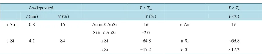
[image:3.595.86.537.627.721.2]TEM images both of as-deposited and annealed thin films are shown in Figure 2. The annealed temperature was 873 K. In the pictures of the cross section of the multilayer, the dark parts reveal the Au layers. In the as-depo- sited thin film, the well-stacked Au and Si layers were observed (Figure 2(a)). By Fourier transform (FT) of atomic arrangement in Figure 2(a), the as-deposited thin film was found to be amorphous. On the other hand, the layered structure completely disappeared after annealing (Figure 2(b)). Instead, Au nanoparticles existed in the thin film, where the nanoparticles randomly locate inside Si. FT of the Au nanoparticles in Figure 2(b) sug-gests that the nanoparticles crystallized from amorphous by annealing. Thus, irreversible morphological trans-formation occurred accompanying by crystallization of the Au nanoparticles (c-Au).
Table 1. Thickness of the multilayer and volume fractions of Au and Si at each state.
As-deposited T > Tm T < Tc
t (nm) V (%) V (%) V (%)
a-Au 0.8 16 Au in ℓ-AuSi 16 c-Au 16
Si in ℓ-AuSi ~2.0
a-Si 4.2 84 a-Si ~64.8 a-Si ~66.8
M. Aono .
Figure 1. Thermal history of in situ observation of X-ray diffraction. Melting point and crystallization temperature at each thermal cycles are expressed by red blue closed circles, respectively. Both heating and cooling rate was 10 K/min. Bulk eutectic point (TEB) is indicated by green line. Thick blue and red lines represent crystal- and liquid-Au,
respectively. Amorphous Au is expressed by thin black line. ML MIC
T is temperature of metal-induced crystallization of a-Si in the multilayer.
Figure 2. Cross-sectional TEM images of (a) the as deposited a-Au/a-Si and (b) the annealed thin film having the c-Au nanoparticles. The annealing temperature is 873 K.
In situ observation using TEM is indispensable to clarify the intermediate process of the above morphological transformation from the multilayer to Au nanoparticles in real space. Upon heating, the layered structure of Au was changing gradually. At 393 K as shown in Figure 3(a), roughness at the boundary between a-Au and a-Si occurred partially on the atomic scale. The modulation of the boundaries in the multilayer implies that Au diffu-sion might be activated thermally below the MIC temperature (TMICML = 450 K). By further heating above
ML MIC T , zigzag patterns were observed at 478 K (=Tzig) with losing the flatness and smoothness (Figure 3(b)). We
sup-pose that, above TMICML, much Au diffusion is promoted on the mesoscopic scale. Consequently, the initial layered
structure of a-Au might be modified into the zigzag one by mass transfer of Au. At 508 K, the metastable zigzag pattern in the thin film vanished drastically (Figure 3(c)). Simultaneously, some dynamic fluctuations of Au nanoparticles were probed by the in situ TEM observation. The nano-heterogeneity is characterized by its am-biguous boundary and dynamic motion. The nearly static zigzag pattern at 478 K and slow dynamic nano-he- terogeneity at 508 K (second order) are regarded as a precursor phenomenon of the Au nanoparticle formation.
3.2. Crystal/Amorphous Estimations by XRD
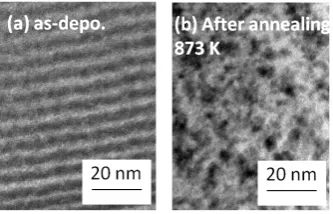
Both the as-deposited Si and Au layers is an amorphous state, which is determined by XRD (Figure 4(a)). In fact, there is no sharp Bragg spot in the 2D X-ray diffraction except for those from the substrate. The weak spots are from the substrate with different wavelengths such as Cu Kβ1 (λ = 0.1392 nm) and W Lα1 (λ = 0.1476 nm)
due to filament of X-ray generator. Judging from no Debye rings, the as-deposited multilayer in Au1−xSix
con-sists only of a-Au and a-Si. In the sample preparations, Au atoms cannot form crystal in the multilayer during deposition, since tAu (=0.8 nm) might be too thin to achieve the critical size for Au crystal nucleation. It is
con-firmed from a previous study using bilayered c-Au/a-Si (tAu = 30 nm) [6], that the Au thickness is sufficient for
the crystal nucleation of Au.
[image:4.595.232.399.291.398.2]M. Aono .
Figure 3. In situ observations by TEM at (a) 393 K, (b) 478 K and (c) 508 K. As a precursor phenomenon to Au nanoparticles, zigzag pattern is formed at around 480 K, whose temperature is equivalent to the Au crystallization temperature determined by XRD. Au nanoparticle appeared at 510 K.
Figure 4. 2D X-ray diffraction patterns (a) before thermal cycle and (b) after cycle 4. The 2D data are reduced into 1D patterns (c) before thermal cycle and (d) after the 4th cycle.
the XRD pattern (Figure 4(b)). From the peak widths, the average size of c-Au nanoparticles was estimated at room temperature and was determined to be 3.0 nm in radius. The ideal Debye rings of the Bragg reflections in Figure 4(b) suggest that the Au nanoparticles have no orientational order in the thin film. Thus, after annealing, the c-Au nanoparticles were observed at random sites by TEM and random crystal orientations by XRD. There-fore, XRD data does not contradict with the TEM observations relating to the morphological transformation from multilayer to Au nanoparticles. To compare the Au crystal with Si one, the observed 2D data were reduced into 1D (Figure 4(c) andFigure 4(d)). Moreover, after cycle 4, metastable Au silicides such as Au2Si, Au5Si2
and Au7Si [8]-[10] were not seen at room temperature (Figure 4(b)). Metastable silicides were bit seen during in situ XRD observations. By Williamson-Hall method [26], local root-mean-square strain of c-Au was analyzed using the thermal cycling sample. From the peak widths of Bragg reflections in c-Au (Figure 4(d)), strain of the c-Au nanoparticles is negligibly small.
3.3. Au Nanoparticle Formation by in Situ XRD
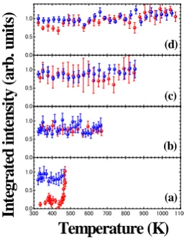
Figures 5(a)-(d) show the respective integrated intensities of Si 111 Bragg reflection at each thermal cycle. At cycle 1, a-Si crystallized partially and irreversibly at around 450 K (=TMICML) (Figure 5(a)). This is regarded as typical MIC, but no Au crystallization was detected. Once the MIC process occurred, the volume of c-Si was almost constant over all thermal cycles (cycles 1 - 4). The irreversible Si crystallization can be interpreted as frozen Si atoms, which are unstably captured in the multilayer, whereas the as-deposited a-Si is partially stabi-lized by crystallization. After cycle 4, XRD in Figure 4(b) and Figure 4(d) reveal that the Bragg intensities of c-Au are larger than those of c-Si in spite of tAu < tSi. For quantitative analysis of each crystal volumes, we
esti-mate the crystal volume ratio by X-ray kinematical theory [27]. Generally, the scattering volume, V, in XRD is proportional to integrated intensities of Bragg reflections. In the case of polycrystal, the relation is given by,
2 2M
hkl hkl e LP hkl
I ∝ F − ⋅ ⋅m ⋅V. (2)
hkl
F is the structure factor and e−2M is the Debye-Waller factor as thermal dumping function. LP is the Lor-entz-polarization factor. mhkl is the multiplicity factor for polycrystalline. Here, we ignore the extinction effect,
M. Aono .
300 400 500 600 700 800 900 1000 1100 0.0 0.5 1.0 (a)
Int
eg
ra
te
d i
nt
ens
it
y
(
a
rb.
uni
ts
)
Temperature (K)
0.0 0.5 1.0 (b) 0.0 0.5 1.0 (c) 0.0 0.5 1.0 (d)Figure 5. Integrated intensities of Si 111 Bragg reflection at (a) cycle 1, (b) cycle 2, (c) cycle 3 and (d) cycle 4. Heating and cooling data are represented by red and blue closed circles, respectively.
due to quite small nanoparticles. When the observed integrated intensities of Bragg reflections are normalized using Equation (2), the substantial volumes ratio of VSi (c-Si) to VAu (c-Au) is evaluated to be 1.07. If all a-Au crystallize, VAu of c-Au becomes 16%. Using the crystal volume ratio, the volume of c-Si is calculated to be 17.2% (Table 1). The rest of Si (66.8%) still remains frozen as the amorphous state even after cycle 4. Hence, a-Si might be stable trivially in the thin film. In addition to small amount of c-Si on the MIC process, lower ML
MIC T (=450 K) was observed in this study. Previously, on heating (3 K/min), the MIC occurred at around 483 K with decreasing Bragg intensity of c-Au in the thin film (30 nm of c-Au on a 200 nm thick a-Si) [6]. Moreover, large grained c-Si was obtained in the study. Therefore, the partial and irreversible MIC at cycle 1 in this study is en-tirely different from the conventional MIC process. Here, we emphasize that an initial Au state (a-Au or c-Au) influences extensively on the MIC process in a-Si.
On heating the film at cycle 2 (Tmax = 673 K), a-Au started to crystallize at around 480 K (=Tc). Figure 6(a)
shows temperature dependence of intensity of Au 111 Bragg reflection. The crystallization temperature of Au coincides with Tzig. In real space, zigzag patterns of Au layers in Figure 3(b) were formed at the same
tempera-ture as a-Au started to crystallize. A significant point is that Au nucleation process has some relation with the morphological changes. From the mass transfer of Au, which is explained by shape change from flat stripe to zigzag, Au diffusion might assist the crystal nucleation. The intensity of Au 111 Bragg reflection gradually in-creased with increasing temperature. The previous study [16] suggests that the morphological transformation from the layered a-Au to the c-Au nanoparticles takes place irreversibly. In contrast to the MIC in a-Si, it is em-phasized that the whole volume of a-Au can transform to c-Au at around 560 K. On deposition process of Au, the confinement in the thin Au layer (tAu = 0.8 nm) below the critical size for crystal nucleation enforces the
atomic arrangement to form unstable amorphous, which is far from an equilibrium state. Consequently, all a-Au can transform to crystal, since the driving force from a-Au to c-Au is large enough. Further heating at cycle 2 caused the eutectic Au1−xSix to melt. Above 570 K, the intensity of c-Au decreased and disappeared completely
at 600 K (= NP m
T ), although the Bragg intensities of c-Si were almost constant. Thus, it is interpreted that liquid AuSi (ℓ-AuSi) was formed with a mass transfer from a-Si (Table 1). Here, the bulk eutectic point ( B
E T ) in Au1−xSix is 636 K. In the same manner with low TMICML, the thin film has a tendency of low
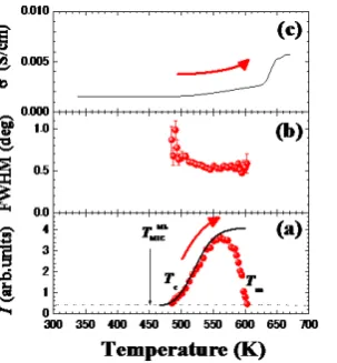
NP m
T . On another ap-proach, temperature dependence of full width at half maximum (FWHM) of Au 111 Bragg reflection is calcu-lated by profile fitting using the asymmetric pseudo-Voigt function (Figure 6(b)). Remarkably, FWHM at the early stage of crystallization became large reflecting on small nuclei from a-Au. Accompanying with coarsening up to the c-Au nanoparticles, FWHM of the Bragg reflection became smaller. At the temperature range from 540 K up to 600 K, constant FWHM implies that the nanoparticle size of c-Au was suppressed at 2.6 nm in radius (robs), which is determined by the conventional Scherrer equation [28].
3.4. Au Diffusion Process at the Early Stage of Au Crystallization
[image:6.595.244.378.84.258.2]M. Aono .
Figure 6. Heating process of (a) intensity, (b) FWHM of Au 111 Bragg reflection at the 2nd heating and (c) electri-cal conductivity, σ. Solid curve reveals the calculated values by the diffusion-driven nucleation model.
electrical conductivity (σ) was measured separately using other as-deposited sample at the same heating rate (10 K/min) inFigure 6(c). At around Tc of c-Au, gradient of the conductivity as a function of temperature varied a
little. Since σ is expressed by mobility of species having charge, it is adequate to consider thermally induced lo-cal diffusion of Au atoms above Tc (~Tzig). The abrupt increase of σ above
NP m
T might be originated from free-Au migration in the liquid state. In order to interpret the irreversible morphological transfer and the slow crystal growth process of Au, we assume the process by introducing the conventional “diffusion-limited model” and “interface-limited model”. Just below Au crystallization temperature, Au diffusion occurs on atomic scale in amorphous multilayer. By the TEM observations, Au diffusion-driven zigzag structure supports the Au mass transfer. At the early stage of crystallization, Au atoms aggregate each other and crystal nanoparticle is formed. At the late stage of crystallization, interface-limited model is effective once size of nanoparticle exceeds the criti-cal size. However, repulsive interaction near the eutectic point suppress the further growth of Au nanoparticle.
We focus the early stage of Au diffusion process. The local diffusion is described by slow dynamics has less geometrical constraint, that is, shape flexibility, compared with the interface-limited process. Then, we introduce the diffusion-assisted nucleation model [29] [30], which is provided by,
( )
2 B Δ , d exp d nG n c P
K c
t k T
= −
, (3)
where kB is the Boltzmann constant and ∆G is the free energy of an n-monomer embryo. P is the size
distribu-tion funcdistribu-tion, which is represented by n-monomer embryo. c is the monomer concentration. In the Smolu-chowski expression, Kn is approximately obtained by,
1 3
4π
n
K = an D. (4)
Here, D is diffusion coefficient for monomers and a is radius of the monomer. In the case of a-Au/a-Si system above Tc, D in Equation (4) corresponds to Au atomic diffusion into a-Si. Experimentally, the activation energy
of Au atomic diffusion inside a-Si was obtained in the previous study [31]. The effective radius of the embryo, r, is expressed as an1/3 considering spherical aggregation of n-monomer [29]. In the XRD experiments, we ob-tained temperature dependence of VAu(T) under the constant heating rate, ∆T/∆t (= 10 K/min). If we assume that the growth curve, VAu(T), has a similarity with time dependence of the volume, VAu(t),
Au Au
d Δ Δ
d Δ Δ
V V T
t ≅ T t is approximately obtained. With satisfying the diffusion-assisted nucleation, the Equation (3) is modified by,
( ) ( ) ( )
{
}
( )
Au 2 B Δ , Δ d exp Δ dG r T
V P
r T D T c T
T t k T
∝ ∝ −
. (5)
M. Aono .
of the observed VAu(T),
(
dVAu dT)
obs, is easily calculated. Also, robs(T) is estimated by FWHM of Bragg reflec-tion (Figure 6(b)). We used D(T) in the previous study [31]. Unknown parameters are ∆G and c(T) in Equation (5). From 480 to 600 K, we assume that ∆G in Equation (5) is approximately expressed by a weak linear relation with temperature (ΔG=k0+k T1 ). Also, it is assumed that c(T) is described by proper function such as tanh
(
)
{
−k T−T0}
. By referring(
)
obs Au
dV dT , the self-consistent calculation can determine the ∆G and c(T) simul- taneously. As a result, the calculated growth curve including diffusion process is exhibited by the solid curve in Figure 6(a). Above 560 K, actual intensity of Au 111 Bragg reflection decreased due to melting. Finally, both experimental results and model calculation supports the idea based on the diffusion-assisted nucleation process of Au. We notice that the initial state of the a-Au/a-Si thin film has major influence on both the irreversible MIC in Si and the Au nano-crystallization. In fact, the relatively slow diffusion of Au was enhanced in a-Si compared with Au diffusion in c-Si [31].
3.5 Reversible Liquid—Au Nanoparticle Transition
If irreversible morphological transformation from the multilayer to Au nanoparticle occurs, the reversible liq-uid-solid phase transition was observed repeatedly. Even above TmNP of c-Au, the whole thin film does not melt,
since c-Si and a-Si existed at Tmax and the flat surface in the thin film was maintained at room temperature after
thermal cycling. Heterogeneous ℓ-AuSi in the thin film above TmNP is the key to understand the reversible
phase transition between the ℓ-AuSi and the c-Au nanoparticles. On cooling at cycle 2, Tc was determined to be
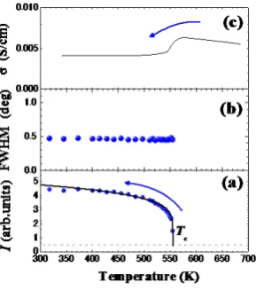
556 K by temperature dependences of intensity and FWHM of Au 111 Bragg reflection (Figure 7(a) and Figure 7(b)). Since small nuclei were not observable in small scattering volume of the thin film, Bragg intensities were derived not from small nuclei, but from the c-Au nanoparticles. A more significant point is that FWHM of the Bragg reflection is invariant on cooling process in Figure 7(b). It is well known that the constant FWHM of Bragg reflection means non-coarsening of a crystal domain [32]. Hence, the population of c-Au nanoparticles is increasing on cooling without crystal domain growth. The behavior is analogous with reversible spin ordering in a ferromagnet. Therefore, we apply the Ising model [33] into the crystallization from the ℓ-AuSi to the c-Au nanoparticles. The feature of the Ising model is that the Hamiltonian is described only by the first nearest neigh- bor interaction. Based on the Ising model, crystallization process is provided by,
( )
Au
c
[image:8.595.241.386.533.697.2]V T ∝T −T β, (6) where β is the critical exponent. By the least square fitting, the experimentally obtained βobs is evaluated to be 0.17. The fitted growth curve is represented by the solid line in Figure 6(a). The exact solution of the 2D Ising model showed the β = 1/8 (=0.125) [33]. In order to investigate the crossover from 2D to 3D property in the Is- ing model, systematic simulations in the thin film [34] were demonstrated, where periodic boundary condition is employed on the x-y planes. Here, the x-y plane is parallel to the substrate and the z direction is perpendicular to
Figure 7. Cooling process of (a) intensity, (b) FWHM of Au 111 Bragg reflection at the 2nd cooling and (c)
M. Aono .
it. In the simulation box denoted by L × L × Nz, the critical exponent βcal becomes 0.17, when L is 160 and Nz is
6. The accordance between βobs and βcal indicates that the nanoparticles without their aggregations are consistent with the ideal spin system with finite thickness along the stacking sequence direction. Also, it is supposed that the actual appearance of the Au nanoparticles obeys short-range order (SRO) interaction. The analogy provides a significant insight into the reversible ℓ-AuSi-c-Au nanoparticle phase transition. Figure 7(c) reveals electrical conductivity on cooling. Vanishing of ℓ-AuSi causes the decrease of the conductivity at around Tc. Below Tc, the
conductivity value became smaller than that on heating as shown in Figure 6(c), which is represented by the ir-reversible transformation from the multilayer to nano particle. At room temperature, the difference between them is originated from the layered a-Au land the isolated Au nanoparticles.
3.6. Thermodynamic Analysis of Au Nanoparticle in Eutectic AuSi
As mentioned earlier, the reversible liquid-solid phase transition in the thin film occurs between heterogeneous ℓ-AuSi and c-Au nanoparticles. When we consider the surface and bulk phases at the equilibrium state, the sur-face tension in binary liquid alloy should be treated thermodynamically. Recently, it is predicted from a ther-modynamical perspective, that spherical particle size [19] [35] is obtained by introducing the surface tension
[36]. The relationships between the observed TmNP and radius of the c-Au nanoparticles (r obs
) were calculated using the basic theory in nano-sized binary alloy system [19] [35]. In in situ XRD, robs in cycle 2 - 4 is obtained by the Scherrer equation as listed in Table 2[28]. While, robs is also determined by direct TEM observations. In fact, the particle size of c-Au has a relation with NP
m
T as shown in Figure 8.
In the theory [19] [35], the spherical particle having radius, r, is connected with TmNP in binary alloy system.
Gibbs energy of bulk (ΔGBulk) and surface (ΔGSurf) in the binary system is given by,
(
)
Bulk L-S L-S ex,L
1 1 2 2 1 1 2 2
ΔG =x GΔ +xΔG +G +RT xlnx +xlnx , (7)
(
)
{
}
Surf L L S S S S
1 1 1 2 2 2
2
ΔG V x V x V
r σ σ σ
= − + . (8)
Here, L-S i
ΔG is Gibbs energy difference between liquid and solid in pure system (i-component: i = 1 or 2), while Gex,L is the excess Gibbs energy of liquid phase in binary system. Surface tension of pure solid is ex-pressed by S
i
σ . σL reveals the surface tension of binary liquid combined with molar volume of the binary liquid, VL. σL is numerically calculated using L
1
σ and L 2
σ . VL is defined by L L 1 1 2 2 x V +x V . L
i
V corresponds to the molar volume for the pure liquid component. In contrast, S
i
σ and S i
V are surface tension and molar volume of pure solid, respectively. It should be noticed that L
i
σ , L i V , S
i
σ and S i
V contain the temperature factor of ( NP
m
T -Tm,i). Tm,i is the melting point in pure system i. If the condition of
Bulk Surf
ΔG +ΔG =0 is satisfied, Equa-tion (8) is modified as,
(
)
{
L L S S S S}
1 1 1 2 2 2 Bulk
2 Δ
r V x V x V
G σ σ σ
= − − + . (9)
Using the temperature factor and Equation (9), the NP m
T at fixing concentration x1 (=1 − x2) is provided
de-pending on the Au nanoparticle radius, r. At xE = 0.186 in AuSi system, the calculated radius of the Au
nanopar-ticle, rcal, is numerically obtained using each TmNP (Table 2). Here, in the calculations, thermodynamic data and
parameters in Au-Si system as previously reported paper [35] are used. Experimentally, ℓ-AuSi, compositional fluctuations occur naturally. If we permit the possible compositional fluctuations, the robs obtained both from XRD and TEM is in good agreement with the rcal within experimental errors (Figure 8). Consequently, in the thin film, the lowering eutectic point of the Au nanoparticle is well explained theoretically.
3.7. Comparison between Irreversible and Reversible Transformations
The scenario of two different irreversible/reversible transformations is illustrated in Figure 9. The irreversible transformation from the layered a-Au to c-Au nanoparticles is distinguished from the reversible liquid-nano- crystal transformation. MIC process of a-Si partially occurred from the as-deposited sample ( ML
M. Aono .
Table 2. Thermal cycle dependence of melting point ( NP m
T ), calculated radius of Au nanoparticle (rcal) and observed one (robs) determined by XRD and TEM. Tmax is the maximum temperature at each thermal cycles.
Cycle Tmax (K) TmNP (K) r
cal (nm) robs XRD (nm) robs TEM (nm)
2nd 673 600 2.2 3.2 3.0
3rd 873 612 3.6 3.8 5.0
4th 1073 621 6.3 4.0 7.5
Figure 8. Thermodynamically calculated melting point in Au1−xSix. Closed red and blue circles reveal the
[image:10.595.86.512.116.177.2]experi-mentally obtained radius by TEM and XRD.
Figure 9. Schematic illustration of morphological transformation from a-Au/Si multilayer to Au nanoparticles.
atomic scale by crystal nucleation of Si, however, crystal nucleation of Au is not induced at this stage.
Next step on heating is that zigzag structure and Au crystallization occurs simultaneously as a precursor phe-nomenon of Au nanoparticle formation (T > Tc - Tzig). As a result of aggregation of diffusing Au atoms, Au
nu-cleation takes place on the off-sites from the original a-Au layers. Remarkably slow temperature evolution of VAu(T) has no discrepancy with time consuming diffusion-driven nucleation. At the same time, shape transfer based on the diffusion-limited model happens in low energy barrier. When the interface-limited process occurs in the morphological transformation, large strain and boundary energy should be considered additionally. In spite of the diffusion-limited motion, all of a-Au is crystallized due to large driving force between amorphous and crystal.
Focusing on the reversible transformation, heterogeneous distribution of a-Si (VSi—66.8%) at Tmax prevents to
melt the whole film (T > Tm). Partially melted ℓ-AuSi region distributes independently in the center of c-Au
[image:10.595.235.389.355.509.2]M. Aono .
nanoparticles. Then, the same reversible phase transition between the ℓ-AuSi and the c-Au nanoparticles occurs repeatedly. Also, less degrees of freedom in the crystallization mechanism leads to the ideal Ising model de-scribed only by simple SRO correlation. The idealized spin system is applied into the spontaneous nucleation and size-limited growth in the thin film.
4. Conclusions
On heating, Au nanoparticle formation process from multilayer was clarified in situ TEM and XRD. The direct observation proves irreversibly morphological transformation from the layered a-Au/a-Si multilayer to the c-Au nanoparticles. As a precursor phenomenon to the Au nanoparticles, the intermediate zigzag patterns in real space were observed by in situ TEM. The zigzag structure was induced by diffusion-assisted Au crystallization. While, reversible transformation between the ℓ-AuSi to the c-Au nanoparticles was obtained by in situ XRD. The re-versible phenomenon is a typical memory effect in the thin film. Heterogeneous eutectic ℓ-AuSi surrounding by deformed a-Si matrix contributes to reproducible appearance of c-Au nanoparticles, whose position and size are almost fixed. VAu(T) as the outstanding memory effect is well explained by the quasi-2D Ising model.
Theoretically, the relation between TmNP and the particle size can support the experimental results in the eutectic AuSi binary system. The size of c-Au from the ℓ-AuSi is proportional to the driving force depending on Tmax at each thermal cycle.
Acknowledgements
We appreciate Dr. Y. Okamoto and Professor Y. Watanabe of National Defense Academy for sample prepara-tions and helpful discussions. This work was supported by NIMS (National Institute for Materials Science, Ja-pan) microstructural characterization platform as a program of “Nanotechnology Platform” of the Ministry of Education, Culture, Sports, Science and Technology (MEXT), Japan.
References
[1] Hiraki, A. (1983)Low Temperature Reactions at Si-Metal Contacts—From SiO2 Growth Due to Si-Au Reaction to the
Mechanism of Silicide Formation. Japanese Journal of Applied Physics, 22, 549-562.
http://dx.doi.org/10.1143/JJAP.22.549
[2] Ito, T. and Gibson, W.M. (1987) Metal/Silicon Reactions Studied by High Energy Ion Scattering. Japanese Journal of Applied Physics, 26, 841-847. http://dx.doi.org/10.1143/JJAP.26.841
[3] Her, Y.-C. and Chen, C.-W. (2007) Crystallization Kinetics of Ultrathin Amorphous Si Film Induced by Al Metal Layer under Thermal Annealing and Pulsed Laser Irradiation.Journal of Applied Physics, 101, Article ID: 043518.
http://dx.doi.org/10.1063/1.2654512
[4] Bokhonov, B. and Korchagin, M. (2000)In Situ Investigation of Stage of the Formation of Eutectic Alloys in Si-Au and Si-Al Systems. Journal of Alloys and Compounds, 312, 238-250.
http://dx.doi.org/10.1016/S0925-8388(00)01173-7
[5] Ehrhardt, J., Klimmer, A., Eisenmenger, J., Müller, Th., Boyen, H.-G., Ziemanna, P., Biskupek, J. and Kaiser, U. (2006) Influence of Ion Induced Amorphicity on the Diffusion of Gold into Silicon. Journal of Applied Physics, 100, Article ID: 063534. http://dx.doi.org/10.1063/1.2259815
[6] Knaepen, W., Detavernier, C., Van Meirhaeghe, R.L., Sweet, J.J. and Lavoie, C. (2008) In-Situ X-Ray Diffraction Study of Metal Induced Crystallization of Amorphous Silicon. Thin Solid Films, 516, 4946-4952.
http://dx.doi.org/10.1016/j.tsf.2007.09.037
[7] Bal, J.K. and Hazra, S. (2007)Interfacial Role in Room-Temperature Diffusion of Au into Si Substrates. Physical Re-view B, 75, Article ID: 205411. http://dx.doi.org/10.1103/PhysRevB.75.205411
[8] Ashtikar, M.S. and Sharma, G.L. (1995) Structural Investigation of Gold Induced Crystallization in Hydrogenated Amorphous Silicon Thin Films. Japanese Journal of Applied Physics, 34, 5520-5526.
http://dx.doi.org/10.1143/JJAP.34.5520
[9] Chromik, R.R., Zavalij, L., Johnson, M.D. and Cotts, E.J. (2002)Calorimetric Investigation of the Formation of Me-tastable Silicides in Au/a-Si Thin Film Multilayers. Journal of Applied Physics, 91, 8992-8998.
http://dx.doi.org/10.1063/1.1432774
M. Aono .
http://dx.doi.org/10.1002/adma.200290017
[11] Shpyrko, O.G., Streitel, R., Balagurusamy, V.S.K., Grigoriev, A.Y., Deutsch, M., Ocko, B.M., Meron, M., Lin, B. and Pershan, P.S. (2007)Crystalline Surface Phases of the Liquid Au-Si Eutectic Alloy. Physical Review B, 76, Article ID: 245436. http://dx.doi.org/10.1103/PhysRevB.76.245436
[12] Pinardi, A.L., Leake, S.J., Felici, R. and Robinson, I.K. (2009)Formation of an Au-Si Eutectic on a Clean Silicon Sur-face. Physical ReviewB, 79, Article ID: 045416. http://dx.doi.org/10.1103/PhysRevB.79.045416
[13] Schülli, T.U., Daudin, R., Renaud, G., Vaysset, A., Geaymond, O. and Pasturel, A. (2010)Substrate-Enhanced Super-cooling in AuSi Eutectic Droplets. Nature, 464, 1174-1177. http://dx.doi.org/10.1038/nature08986
[14] Chandra, A. and Clemens, B.M.J. (2004)Monodisperse Nanoparticles via Metal Induced Crystallization. Journal of Applied Physics, 96, 6776-6781. http://dx.doi.org/10.1063/1.1812817
[15] Venkatachalam, D.K., Fletcher, N.H., Sood, D.K. and Elliman, R.G. (2009)Self-Assembled Nanoparticle Spirals from Two-Dimensional Compositional Banding in Thin Films. Applied Physics Letters, 94, Article ID: 213110.
http://dx.doi.org/10.1063/1.3143666
[16] Aono, M., Takahashi, M., Takiguchi, H., Okamoto, Y., Kitazawa, N. and Watanabe, Y. (2012)Thermal Annealing of a-Si/Au Superlattice Thin Films. Journal of Non-Crystalline Solids, 358, 2150-2153.
http://dx.doi.org/10.1016/j.jnoncrysol.2011.12.088
[17] Miyazaki, H., Takiguchi, H., Aono, M. and Okamoto, Y. (2012)Influence of Annealing Temperature and Au Concen-tration on the Electrical Properties of Multilayered a-Ge/Au Films. Journal of Non-Crystalline Solids, 358, 2103-2106.
http://dx.doi.org/10.1016/j.jnoncrysol.2012.01.064
[18] Stockman, M.I. (2010)Nanoscience: Dark-Hot Resonances. Nature, 467, 541-542.
[19] Derkacs, D., Lim, S.H., Matheu, P., Mar, W. and Yu, E.T. (2006)Improved Performance of Amorphous Silicon Solar Cells via Scattering from Surface Plasmon Polaritons in Nearby Metallic Nanoparticles. Applied Physics Letters, 89, Article ID: 093103. http://dx.doi.org/10.1063/1.2336629
[20] Fujiki, A., Uemura, T., Zettsu, N., Akai-Kasaya, M., Saito, A. and Kuwahara, Y. (2010)Enhanced Fluorescence by Surface Plasmon Coupling of Au Nanoparticles in an Organic Electroluminescence Diode. Applied Physics Letters, 96, Article ID: 043307. http://dx.doi.org/10.1063/1.3271773
[21] Cheng, C.W., Sie, E.J., Liu, B., Huan, C.H.A., Sum, T.C., Sun, H.D. and Fan, H.J. (2010)Surface Plasmon Enhanced Band Edge Luminescence of ZnO Nanorods by Capping Au Nanoparticles. Applied Physics Letters, 96, Article ID: 071107. http://dx.doi.org/10.1063/1.3323091
[22] Wu, T.H., Kuo, P.C., Ou, S.L., Chen, J.P., Yen, P.F., Jeng, T.R., Wu, C.Y. and Huang, D.R. (2008)Diffusion and Cry- stallization Mechanisms of Ge/Au Bilayer Media for Write-Once Optical Disk. Applied Physics Letters, 92, Article ID: 011126. http://dx.doi.org/10.1063/1.2831690
[23] Guzman, J., Boswell-Koller, C.N., Beeman, J.W., Bustillo, K.C., Conry, T., Dubón, O.D., Hansen, W.L., Levander, A. X., Liao, C.Y., Lieten, R.R., Sawyer, C.A., Sherburne, M.P., Shin, S.J., Stone, P.R., Watanabe, M., Yu, K.M., Ager III, J.W., Chrzan, D.C. and Haller, E.E. (2011)Reversible Phase Changes in Ge-Au Nanoparticles. Applied Physics Letters, 98, Article ID: 193101. http://dx.doi.org/10.1063/1.3584850
[24] Siegel, J., Lyutakov, O., Rybka, V., Kolská, Z. and Švorčík, V. (2011)Properties of Gold Nanostructures Sputtered on Glass. Nanoscale Research Letters, 6, 96-99. http://dx.doi.org/10.1186/1556-276X-6-96
[25] Alvarez, F., Díaz, C.C., Valladares, A.A. and Valladares, R.M. (2002)Radial Distribution Functions of ab Initio Gen-erated Amorphous Covalent Networks. Physical ReviewB, 65, Article ID: 113108.
http://dx.doi.org/10.1103/PhysRevB.65.113108
[26] Mittemeijer, E.J., Welzel, U. and Kristallogr, Z. (2008)The “State of the Art” of the Diffraction Analysis of Crystallite Size and Lattice Strain.Zeitschrift für Kristallographie, Crystalline Materials, 223, 552-560.
http://dx.doi.org/10.1524/zkri.2008.1213
[27] Warren, B.E. (1990) X-Ray Diffraction. Dover, New York.
[28] Ida, T., Shimazaki, S., Hibino, H. and Toraya, H. (2003)Diffraction Peak Profiles from Spherical Crystallites with Lognormal Size Distribution. Journal of Applied Crystallography, 36, 1107-1115.
http://dx.doi.org/10.1107/S0021889803011580
[29] Robb, D.T. and Privman, V. (2008)Model of Nanocrystal Formation in Solution by Burst Nucleation and Diffusional Growth. Langmuir, 24, 26-35. http://dx.doi.org/10.1021/la702097g
[30] Privman, V. (2008)Diffusional Nucleation of Nanocrystals and Their Self-Assembly into Uniform Colloids. Journal of Optoelectronics and Advanced Materials, 10, 2827-2839.
M. Aono .
[32] Abe, H., Ishibashi, M., Ohshima, K., Suzuki, T., Wuttig, M. and Kakurai, K. (1994)Kinetics of the Martensitic Transi-tion in In-Tl Alloys. Physical ReviewB, 50, 9020-9024. http://dx.doi.org/10.1103/PhysRevB.50.9020
[33] Onsager, L. (1944)Crystal Statistics. I. A Two-Dimensional Model with an Order-Disorder Transition. Physical Re-view, 65, 117-149. http://dx.doi.org/10.1103/PhysRev.65.117
[34] Phu, X.T.P., Ngo, V.T. and Diep, H.T. (2009)Critical Behavior of Magnetic Thin Films. Surface Science, 603, 109- 116. http://dx.doi.org/10.1016/j.susc.2008.10.037
[35] Tanaka, T. (2010)Prediction of Phase Diagrams in Nano-Sized Binary Alloys. Materials Science Forum, 653, 55-75.
http://dx.doi.org/10.4028/www.scientific.net/MSF.653.55