© 2016, IRJET | Impact Factor value: 4.45 | ISO 9001:2008 Certified Journal | Page 1083
LOW POWER COMPARATOR USING DOUBLE TAIL GATE TECHNIQUE
Sagar. S. Pathak
1, Swapnil. S. Patil
2,Kumud. G. Ingale
3, Prof. D. S. Patil
41Pursuing M. Tech, Dept. of Electronics and Engineering, NMU, Maharashtra, India.
2Pursuing M. Tech, Dept. of Electronics and Engineering, NMU, Maharashtra, India.
3Pursuing M.Sc., Dept. of Electronics, NMU, Maharashtra, India. 4Professor, Dept. of Electronics and Engineering, NMU, Maharashtra, India
---***---Abstract
- The need for low-power, are efficient, a highspeed ADCs is pushing toward the use of dynamic reformative comparators to maximize speed and power efficiency. An analysis on the delay of the dynamic comparators will be presented and logical expressions are derived. From the investigative expressions, designers can obtain an intuition about the main donors to the comparator delay and fully explore the transactions in dynamic comparator design. Based on the presented analysis, a new dynamic comparator is proposed, where the circuit of a predictable double tail comparator is altered for low-power and fast operation even in small supply voltages. Without thwarting the design and by adding few transistors, the positive advice during the regeneration is reinforced, which results in remarkably reduced delay time. It is shown that in the proposed dynamic comparator both the power feasting and delay time are significantly reduced. The design and analysis is performed using 22 nm, 32 nm and 45 nm CMOS technology in Tanner EDA Tool
Key Words: Double-tail comparator, dynamic clocked comparator, high-speed analog-to-digital converters (ADCs), low-power analog design, Tanner EDA Tool
1.INTRODUCTION
Comparators are mostly used in electronic
components after operational amplifiers. Comparators are also known as 1-bit ADCs. So they are mostly used in large wealth in A/D converter. In the analog-to-digital conversion process, it is necessary to trial the input. This sampled signal is applied to comparators, to regulate the digital equivalent of the analog signal. In today’s world, transferrable battery operator devices are increasing, because of low power policies are used for high speed applications. Power reduction can be realized by moving towards smaller size processes. However, as we move towards smaller feature size, these process disparities and other non-idealities will greatly affect the overall performance of the device. One such application where low power degeneracy, low noise, high speed, less hysteresis, less Offset voltage is required to Analog to Digital converters for mobile and portable devices. The precision ofcomparators is defined by its offset, along with power consumption, haste is of keen interest in achieving global higher performance of ADCs. In the past, pre-amplifier based comparators are used for ADC styles such as flash and pipeline. The main drawback of pre-amplifier based comparator is its offset voltage. To overcome these unruly, dynamic comparators are often used to make a judgement once every clock period and require much less offset voltage. However, these dynamic comparators are ached from large power dissipation compared to pre-amplifier based comparators. The main problem of these dynamic comparators is the output signal of latch stage is shifting during clock transition. This is happening due to the presence of noise at input terminals. The propose inverter based disparity amplifier topology eliminates the noise at input side. It also reduces the delay and power consumption.
[image:1.595.308.583.475.691.2]2.Conventional Dynamic Comparator
Fig. 1. Schematic diagram of the conservative dynamic comparator.
During the reset phase when CLK = 0 and Mtail is off, reset transistors (M7–M8) tug both output nodes Outn
© 2016, IRJET | Impact Factor value: 4.45 | ISO 9001:2008 Certified Journal | Page 1084 a valid logical level during reset. In the comparison
phase, when CLK = VDD, transistors M7 and M8 are off, and Mtail is on. Output voltages (Outp, Outn), which had been pre-charged to VDD, start to discharge with different liquidating rates depending on the matching input voltage (INN/INP). Pretentious the case where
VINP > VINN, Outp discharges faster than Outn, hence when Outp (discharged by transistor M2 drain current), falls down to VDD–|Vthp| before Outn
(discharged by transistor M1 drain current), the corresponding pMOS transistor (M5) will turn on initiating the latch revival caused by back-to-back inverters (M3, M5) and M4, M6). Thus, Outn pulls to
VDD and Outp discharges to ground. If VINP < VINN, the circuits work vice versa. As shown in Fig. 2, the delay of this comparator is comprised of two time delays, t0 and tlatch. The delay t0 represents the capacitive discharge of the load capacitance CL until
the first p-channel transistor (M5/M6) turns on. In case, the voltage at node INP is bigger than INN (i.e.,
[image:2.595.307.579.98.358.2]VINP > VINN), the drain current of transistor M2 (I2) causes faster discharge of Outp node compared to the Outn node, which is driven by M1 with smaller current.
Fig. 2. Fleeting simulations of the conventional dynamic comparator for input voltage difference
[image:2.595.34.297.407.692.2]3.Conventional Double-Tail Dynamic Comparator
Fig. 3. Schematic diagram of the conservative double-tail dynamic comparator.
The dual tail enables both a large current in the latching stage and wider Mtail2, for fast latching independent of the input common-mode voltage (Vcm), and a small current in the input stage (small Mtail1), for low offset [10]. During retune phase (CLK = 0,
Mtail1, and Mtail2 are off), transistors M3-M4 pre-charge fn and fp nodes to VDD, which in turn causes transistors MR1 and MR2 to discharge the output nodes to ground. During executive phase (CLK =VDD,
Mtail1 and Mtail2 turn on), M3-M4 turn off and voltages at nodes fn and fp start to drop with the rate defined by IMtail1/Cfn(p) and on top of this, an input-dependent differential voltage _Vfn(p) will build up. The intermediate stage formed by MR1 and MR2 passes Vfn(p) to the cross coupled inverters and also provides a good protecting between input and output, resulting in reduced value of reward noise [10]. Similar to the conventional dynamic comparator, the delay of this comparator comprises two main parts, t0 and
© 2016, IRJET | Impact Factor value: 4.45 | ISO 9001:2008 Certified Journal | Page 1085 Fig. 4. Temporary simulations of the conventional
double-tail dynamic comparator for input voltage difference.
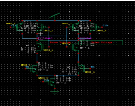
4. PROPOSED DOUBLE-TAIL DYNAMIC COMPARATOR
Fig. 5. Schematic diagram of the proposed dynamic comparator.
During reset phase (CLK = 0, Mtail1 and Mtail2 are off, ducking static power), M3 and M4 pulls both fn and fp nodes to VDD, hence transistor Mc1 and Mc2 are cut off. Interim stage transistors, MR1 and MR2, reset both latch outputs to ground. During decision-making phase (CLK = VDD, Mtail1, and Mtail2 are on), transistors M3 and M4 turn off. Additionally, at the beginning of this phase, the control transistors are still off (since fn and fp are about VDD). Thus, fn and fp start to drop with different rates according to the input voltages. Suppose
[image:3.595.307.572.361.700.2]VINP > VINN, thus fn drops faster than fp, (since M2 provides more current than M1). As long as fn continues sinking, the agreeing pMOS control transistor (Mc1 in this case) starts to turn on, pulling fp node back to the VDD; so another control transistor (Mc2) remains off, allowing fn to be liquidated completely.
[image:3.595.37.286.431.727.2]© 2016, IRJET | Impact Factor value: 4.45 | ISO 9001:2008 Certified Journal | Page 1086 Table: Results
At 45nm Power Dissipated
Delay
Single Tail Comparator
7.056 e-6W 1.245 e-5
Double Tail Comparator
8.872 e-11W 4.258 e-8
Proposed Comparator
5.496 e-11W 5.848 e-8
At 32nm Power Dissipated Delay
Single Tail Comparator
5.431 e-6W 4.257 e-6
Double Tail Comparator
4.790 e-11W 4.659 e-8
Proposed Comparator
5.961 e-13W 8.264 e-8
At 22nm Power Dissipated Delay
Single Tail Comparator
2.348 e-7W 2.367 e-7
Double Tail Comparator
8.628 e-11W 7.368 e-9
Proposed Comparator
7.127 e-13W 9.381 e-11
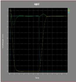
Chart -1Simulation of Modified Double Tail Dynamic Comparator
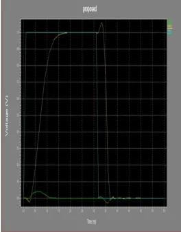
Chart -2 Simulation of proposed body driven Dynamic Comparator
3. CONCLUSIONS
© 2016, IRJET | Impact Factor value: 4.45 | ISO 9001:2008 Certified Journal | Page 1087 REFERENCES
[1] B. Goll and H. Zimmermann, “A comparator with reduced delay time in 65-nm CMOS for supply voltages down to 0.65,” IEEE Trans. CircuitsSyst. II, Exp. Briefs, vol. 56, no. 11, pp. 810–814, Nov. 2009.
[2] S. U. Ay, “A sub-1 volt 10-bit supply boosted SAR ADC design in standard CMOS,” Int. J. Analog Integr. Circuits Signal Process., vol. 66, no. 2, pp. 213–221, Feb. 2011.
[3] A. Mesgarani, M. N. Alam, F. Z. Nelson, and S. U. Ay, “Supply boosting technique for designing very low-voltage mixed-signal circuits in standard CMOS,” in
Proc. IEEE Int. Midwest Symp. Circuits Syst.Dig. Tech. Papers, Aug. 2010, pp. 893–896.
[4] B. J. Blalock, “Body-driving as a Low-Voltage Analog Design Technique for CMOS technology,” in Proc. IEEE Southwest Symp. Mixed-Signal Design, Feb. 2000, pp. 113–118.
[5] M. Maymandi-Nejad and M. Sachdev, “1-bit quantiser with rail to rail input range for sub-1V __
modulators,” IEEE Electron. Lett., vol. 39, no. 12, pp. 894–895, Jan. 2003.
[6] Y. Okaniwa, H. Tamura, M. Kibune, D. Yamazaki, T.-S. Cheung, J. Ogawa, N. Tzartzanis, W. W. Walker, and T. Kuroda, “A 40Gb/s CMOS clocked comparator with bandwidth modulation technique,” IEEE J. Solid-State Circuits, vol. 40, no. 8, pp. 1680–1687, Aug. 2005. [7] B. Goll and H. Zimmermann, “A 0.12 μm CMOS comparator requiring 0.5V at 600MHz and 1.5V at 6 GHz,” in Proc. IEEE Int. Solid-StateCircuits Conf., Dig. Tech. Papers, Feb. 2007, pp. 316–317.
[8] B. Goll and H. Zimmermann, “A 65nm CMOS comparator with modified latch to achieve 7GHz/1.3mW at 1.2V and 700MHz/47μW at 0.6V,” in
Proc. IEEE Int. Solid-State Circuits Conf. Dig. Tech. Papers, Feb. 2009,pp. 328–329.
[9] B. Goll and H. Zimmermann, “Low-power 600MHz comparator for 0.5 V supply voltage in 0.12 μm CMOS,”
IEEE Electron. Lett., vol. 43, no. 7, pp. 388–390, Mar. 2007.
[10] D. Shinkel, E. Mensink, E. Klumperink, E. van Tuijl, and B. Nauta, “A double-tail latch-type voltage sense amplifier with 18ps Setup+Hold time,” in Proc. IEEE Int. Solid-State Circuits Conf., Dig. Tech. Papers, Feb. 2007, pp. 314–315.
[11] P. Nuzzo, F. D. Bernardinis, P. Terreni, and G. Van der Plas, “Noise analysis of regenerative comparators for reconfigurable ADC architectures,” IEEE Trans. Circuits Syst. I, Reg. Papers, vol. 55, no. 6, pp. 1441– 1454, Jul. 2008.
[12] A. Nikoozadeh and B. Murmann, “An analysis of latched comparator offset due to load capacitor mismatch,” IEEE Trans. Circuits Syst.II, Exp. Briefs, vol. 53, no. 12, pp. 1398–1402, Dec. 2006.
[13] S. Babayan-Mashhadi and R. Lotfi, “An offset cancellation technique for comparators using body-voltage trimming,” Int. J. Analog Integr.Circuits Signal Process., vol. 73, no. 3, pp. 673–682, Dec. 2012.
[14] J. He, S. Zhan, D. Chen, and R. J. Geiger, “Analyses of static and dynamic random offset voltages in dynamic comparators,” IEEE Trans.Circuits Syst. I, Reg. Papers, vol. 56, no. 5, pp. 911–919, May 2009.
[15] J. Kim, B. S. Leibowits, J. Ren, and C. J. Madden, “Simulation and analysis of random decision errors in clocked comparators,” IEEE Trans.Circuits Syst. I, Reg. Papers, vol. 56, no. 8, pp. 1844–1857, Aug. 2009. [16] P. M. Figueiredo and J. C. Vital, “Kickback noise reduction technique for CMOS latched comapartors,”
IEEE Trans. Circuits Syst. II, Exp.Briefs, vol. 53, no. 7, pp. 541–545, Jul. 2006.
[17] B. Wicht, T. Nirschl, and D. Schmitt-Landsiedel, “Yield and speed optimization of a latch-type voltage sense amplifier,” IEEE J. Solid-StateCircuits, vol. 39, no. 7, pp. 1148–1158, Jul. 2004.
BIOGRAPHIES
Sagar Sunil Pathak was born in Maharashtra, India. He received the B.E. degrees in Electronics and Telecommunication engineering from the North Maharashtra University of Maharashtra, India in 2014 and currently pursuing the
M.Tech. degree, from the
Department of Electronics