uCube: Control Platform for Power Electronics
A. Galassini, G. Lo Calzo, A. Formentini, C. Gerada, P. Zanchetta, and A. Costabeber
Abstract—This paper presents a versatile tool for development, control and testing of power electronics converters. In the last decade, many different expensive off-the-shelf tools for rapid prototyping and testing have been developed and commercialised by few market players. Recently, the increasing diffusion of low cost, Do It Yourself targeted development tools gained market shares previously controlled by conventional players. This trend has been driven by the fact that, despite their lower performances, many of these low cost systems are powerful enough to develop simple power electronics systems for learning and teaching purposes. This paper describes a control platform developed within the University of Nottingham, targeting at the market and application segment in between the expensive off-the-shelf control boards and the low cost emerging systems. The platform is based on the Microzed evaluation board, equipped with the Xilinx Zynq System-on-Chip. Its flexibility, features and performances will be addressed and examples of how they are being experimentally validated on different rigs will be provided.
Index Terms—Power Electronics, Control board, Control plat-form, Power converters, Zynq, Microzed, uCube, Control
I. INTRODUCTION
The controller may be considered as one of the key elements of every power electronics system. In industrial application, the controller is almost always custom made, designed to be as cheap as possible and tailored on the specific application it will be used with. On the opposite side, in research and development laboratories, both industrial and academic, it is often required to have a versatile and powerful platform, relatively simple to use and offering a good level of debugging. Based on these requirements, different controllers are present on the market as off-the-shelf products. Among the main market players, dSpace controllers represent a well known example, as they offer a wide range of different solutions and their utilization is quite common in the research world [1]–[3]. Another widely diffused solution is theCompactRIOproduced by National Instruments [4], [5]. Its built-in integration with LabView, a graphical PC software mainly intended for virtual instrumentation programming, makes it a good starting point for medium complexity applications. Even if conceptually different from a pure controller product, it’s worth to name for the sake of completeness some of the majors Hardware In the Loop (HIL) products actually present on the market, as they present as well controller capabilities. In this family, the main players can be identified in Typhon HIL [6], OpalRT [7] and, recently, Plexim [8]. The main drawback of these commercial control platforms, often limiting their full diffusion, can be
All the authors are with the Power Electronics, Machine and Control group (PEMC), The University of Nottingham, United Kingdom.
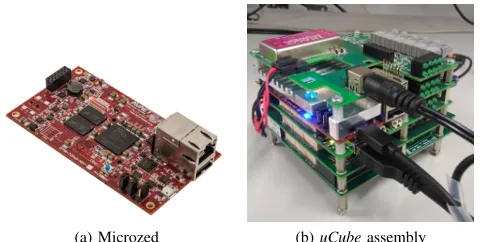
[image:1.612.319.559.154.275.2](a) Microzed (b)uCubeassembly Fig. 1. The Avnet Microzed board (a) and the uCube control board (b)
found in the price. To face this problem, different research group are recently moving towards custom platform [9], [10]. In this paper, a custom made flexible and research oriented control board developed at the University of Nottingham and nameduCube(Fig.1b) will be presented. TheuCubeis based on the off-the-shelf Microzed board [11] from Avnet (Fig.1a), a low-cost development board based on the Xilinx Zynq-7000 All Programmable SoC. The Zynq is a heterogeneous SoC [12] integrating in a single device a dual-core ARM Cortex-A9 based Processing System (PS) and a Field Programmable Gate Array (FPGA) Programmable Logic (PL) [13], [14].
In not heterogeneous systems, where a separate Micro Controller Unit (MCU), or a Digital Signal Processor (DSP), is used in conjunction with a FPGA device, it often happens that the data communication between these two entities represents a serious bottleneck in terms of performance. In fact, in presence of an external communication bus between the two packages, the data clock frequency has to be limited in the range of few tens of mega-hertz. The SoC Zynq family pro-vides on-chip, high bandwidth (up to 150 MHz), low latency AXI interfaces to connect PS and PL and the possibility for the FPGA to direct access system memory for very fast data transfers.
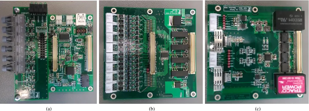
applica-(a) (b) (c)
Fig. 2. (a) FO-PSU-COM expansion board. (b) Analogue-to-Digital Converters expansion board. (c) Resolver and Incremental/Absolute Encoder board
tions and provides for a sin-cos resolver interface and abso-lute/incremental encoder interface. System configuration and software architecture are based on the XAPP1078 application note from Xilinx [15] where the CPU0 is running Petalinux - a GNU/Linux OS baked by Xilinx. Signals coming from and directed to the expansion boards are routed to the FPGA circuitry. Once stored in the form of digital data, they will be used by the two ARM cores to execute the real time control algorithm, also referred at as bare-metal application running on CPU1, and for data exchange with a PC running a specifically designed Matlab Graphical User Interface (GUI).
In the next sections, details of the components building up the uCube will be provided: Section II will describe in more detail the three expansion boards, Section III will see instead a description of the adopted software architecture, while Section IV will presents some examples of the use of uCube in experimental test rigs for motor drive applications. Conclusions and considerations about future developments will be drawn in Section V.
II. EXPANSION BOARDS
TheuCubecontrol platform presents three expansion boards shown in Fig. 2 intended to fully take advantage of the flexibility of the Xilinx Zynq SoC.
A. Fibre Optics, Power supplies and Communications (FO-PSU-COM) expansion board
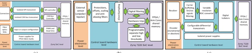
The conceptual scheme of the FO-PSU-COM expansion board is depicted in Fig. 3a. As can be seen, the board provides in addition to the connectivity solutions already present on the Microzed board, an isolated SPI transceiver and an isolated CAN bus transceiver. The isolated SPI transceiver is intended for low throughput data communications (as can be the ones with an external display) and is based on the Linear Technology LTC6820 integrated circuit (IC). The proprietary LTC6820 transmission protocol allows for 1Msps communi-cations on cable length up to 10m (100m with performance
de-rating). The isolated CAN bus transceiver is instead based on the Analog Devices ADM3053BRWZ IC, with 2.5 kVrms isolation. The FO-PSU-COM expansion board is also equipped with the circuitry required to drive up to 24 fibre optics based channels, allowing for the flexibility to configure them as inputs or outputs and to drive different baud rates capable transceiver by simply replacing one component in the circuit. Visual feedback of the fibre optics status is provide as well for quick reference by means of buffered LEDs. Additionally, the board hosts two fast response dc-dc converter to power the FPGA internal banks, properly sequenced to avoid damages to the Microzed board and high in-rush currents at star-tup. The overall aspect of the FO-PSU-COM expansion board is depicted in Fig. 2a
B. Analogue-to-Digital Converters expansion board
[image:2.612.59.552.60.237.2](a) (b) (c)
Fig. 3. (a) FO-PSU-COM conceptual scheme. (b) ADC conceptual scheme. (c) Resolver and Incremental/Absolute Encoder conceptual scheme
PL, lead to an increase in the available Effective Number Of Bits (ENOB). Moreover, in the actual uCube design, the high sampling rate of the ADC ICs as well as the high clock frequency the PL is operated at, have been used in guise of hardware monitors instead of conventionally adopted analogue trip circuits. Reading the current ADC result is possible to evaluate, with a delay of a fraction of microsecond, a fault condition as e.g. over-current or over-voltage, bringing the system to a safe condition promptly and automatically. Each of the 16 channels has been designed to be completely independent from the other, as can be noted from Fig. 2b. This, with respect to multiplexed channels ADC architectures, grants the full performance whatever is the number of ADC channels used in the actual application, as all the channels are acquired at the same time.
C. Resolver/Encoder expansion board
The conceptual scheme of the board is depicted in Fig. 3c. The part related to the resolver interface is built around the Analog Devices AD2S1210 IC. The AD2S1210 is a complete 10-bit to 16-bit resolution tracking resolver-to-digital converter (RDC), integrating an on-board programmable sinusoidal os-cillator that provides sine wave excitation for resolvers, and a type II servo loop to track the inputs and convert the input sine and cosine information into a digital representation of the input angle and velocity. Its variable resolution allows to accommodate, as will be shown in Section IV, applications with different speed ranges. As it has been done for the LTC2313-14 ICs on the Analogue-to-Digital Converters ex-pansion board, the AD2S1210 IC has been digitally interfaced to the system through an additional SPI interface implemented in the FPGA. On the analogue side, a buffer circuit has been designed to boost (both in voltage and in current) the excitation signal internally generated by the AD2S1210, allowing the use of virtually any commercially available synchro-resolver transducer available on the market. For the sin and cos signals, instead, specific scaling circuits and both differential and common-mode filters have been designed, in order to reduce the possibility of issues due to switching noise pick-up. The encoder part of the board is conceptually simpler than its resolver counterpart as, being the encoders transducers intrinsically digital, only differential transducers have been
added, leaving the management of the encoder (absolute or incremental) to a specific logic implemented in the FPGA. Because of the proximity to high voltage areas (machine windings) of this type of feedback sensors, the entire board has been isolated from the remaining stack by means of 3kV digital isolators and 4.5kV dc-dc power supplies. The overall appearance of the Resolver/Encoder expansion board is shown in Fig. 2c.
III. SOFTWARE ARCHITECTURE
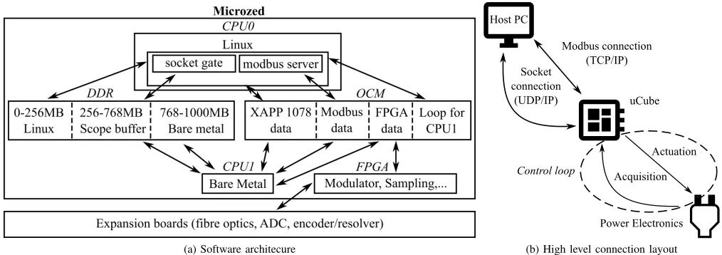
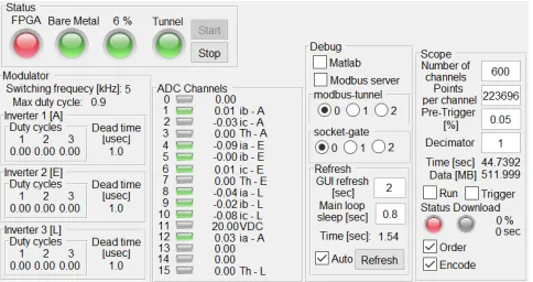
In the proposeduCube control platform, the full flexibility and potential of the Zynq SoC have been obtained by coding specific software for each entity available in the SoC (CPU0, CPU1, and FPGA), as depicted in Fig.4a. Data exchange has been achieved sharing On-Chip Memory (OCM) and Double Data Rate Synchronous Dynamic Random Access Memory (DDR SDRAM). All the hardware elements detailed in the previous section have been physically connected to the FPGA pins and custom software modules have been implemented for each expansion board. On the CPU1, real time bare metal code (or firmware) implementing the control algorithm scheme for the connected power electronics converter(s) is executed (Fig.4b). During start-up operation, Linux is loaded on CPU0. While supervising the whole system, Linux is in charge of handling Host PC communication (Fig.4b). Acquired data, parameter and set-point input forms are presented to the final user thanks to a Matlab Graphical-User-Interface (GUI) shown in Fig. 5. In the next subsections, software components and core interactions will be described in detail.
A. FPGA
[image:3.612.52.575.60.171.2](a) Software architecure (b) High level connection layout
Fig. 4. TheuCubesoftware architecure in Fig.4a has been derived by the XAPP1078 application note from Xilinx. The Host PC in Fig. 4b is used for setting control parameters, on/off flags, set-points and for saving and eventually plotting acquired data and derived variables.
between the IC and the PS, simplifying its configuration and position and speed acquisitions. To communicate with absolute encoders, a BiSS (bidirectional/serial/synchronous) interface up to 10 MHz has been implemented with Cyclic Redundancy Check (CRC).
In the current control board version, three three-phase modulators have been coded in the PL, featuring independently configurable switching frequencies and dead-times. Each mod-ulator uses 7 fibre optics channels to control the inverter gate drives (six legs and a possible braking leg). The remaining 3 channels are configured as independent fault inputs.
The FPGA also implements a trip mechanism to protect the system under unwanted and potentially harmful operating system conditions. Every value acquired from each ADC channel is continuously compared against a low and a high, PS configurable, threshold. If the received value exceeds one of these two thresholds, a fault is asserted, the PWM units turned off and all the outputs brought to the off state with a delay of less then one microsecond. This time is usually sufficient to protect the power electronics converter(s) even in case of shot-through fault.
B. Bare metal
At the system power-up, the FPGA starts in configuration mode waiting for the PS finishing to configure the system. This procedure is carried out using a General Purpose AXI port. When all the peripherals have been set-up the PL is put in running mode. At each sample time all the hardware-related data are read and transferred in the OCM using the Accelerator Coherency Port (ACP) [13]. When the transfer is completed an interrupt is generated for the CPU1 that executes the bare metal code, copy the data to be passed to the PL in OCM and signals back the end of the execution. At that point data are read from the PL and prepared to be applied at the next sample time. Thanks to the very high baud-rate Zynq bus, writing and reading back the data from OCM takes less then
1 microsecond resulting in a very small communication over-head and permitting therefore a very high sample frequency. A watchdog mechanism is also implemented to handle bare metal deadlock and overrun.
The real-time bare metal C code runs in CPU1. It is executed at each sample time and it usually implements the core control algorithms. A complete function library has been developed to handle the communication with the PL and speed-up the coding. It also includes a scope functionality: a configurable number of system variables can be recorded every sample time (or its multiple in down-sampling mode) and stored in memory. Thanks to the high dimension RAM available on the Microzed and the high bandwidth communications described in the next sub-section, the scope system allows an high number of signals and variables to be monitored, simplifying considerably the debugging process.
C. Linux
The main Linux tasks are the following:
• Starting and stopping the bare metal application; • Checking if the bare metal is running or not; • Printing redirected output bare metalprintf function; • Forwarding modbus data from the Host PC to the bare
metal application (and vice-versa) through the OCM thanks to the modbus server (Fig.4a,4b);
• Serving UDP/IP socket connection for downloading the scope buffer within DDR memory through thesocket gate user space process (Fig.4a,4b).
Fig. 5. Bare metal, hardware, and scope buffer status together with set-point, parameter, and flag input forms are shown to the final user on a Matlab GUI.
implemented using TCP/IP over Ethernet or asynchronous serial transmission over a variety of media (EIA/TIA-232-E, EIA-422, EIA/TIA-485-A, etc.). Two physical links have been set-up: the 10/100/1000 Ethernet port and the USB Host 2.0 port thanks to the Remote Network Driver Interface Specification (RNDIS) present in Linux kernel. The modbus server running on Linux has been coded linking against the open-source libmodbus Clibrary [17].
Once the bare metal scope routine is triggered and the acquisition is done, thesocket gateLinux process starts serving recorded data into the scope buffer within DDR memory through UDP/IP socket (Fig.4).
D. Host PC
On the Host PC, the modbus client has been embedded into a C daemon process (called modbus tunnel) forwarding information between the modbus client and a local socket (and vice-versa).
In this way, the so called modbus tunnel allows theuCubeto be queried with any programming language with local socket support. In order to present many different information to the final user, a Matlab GUI interface has been created (Fig. 5).
Whilst only few kilo-Bytes can be addressed by the Modbus protocol, 512MB DDR memory have been assigned to the scope buffer where real time data and derived variables can be saved. Firstly, once the acquisition is done, data are transferred from DDR to the Host PC through the Ethernet or the USB Host 2.0 (3.5MB/sec) port. Secondly, data are saved and even-tually processed and plotted by a custom Matlab script coded by the final user. Furthermore, after every acquisition, modbus data are dumped and saved into a .pdf file automatically generated on the host PC.
IV. EXPERIMENTAL VALIDATION
TheuCubehas been already tested on different experimental rigs. In this work just few of them are reported.
A. Multi-three phase motor
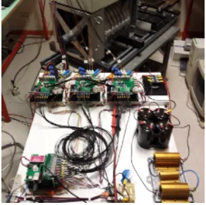
uCube development and testing have been mainly carried out on a rig for studying new multi-drive control strategies. The uCube is currently being used to validate a novel droop
[image:5.612.55.297.50.178.2]control strategy suitable for multi-three phase motors pre-sented in [18]. In Fig. 6, three full bridge converters, built using the off-the-shelf IRMD22381Q evaluation board [19], and connected to a multi-three phase two pole synchronous generator with three sets of windings for a total power of 22kW are shown. Switching and interrupt frequency have been set to10kHz. DC-link voltage has been set to350V. In Fig. 7, the nine phase currents of the motor under a load step variation are shown. Currents are shifted by an angleα=π/9. Data have been recorded by the bare metal application into the scope buffer within DDR memory and then downloaded thanks to thesocket gateLinux process.
B. 80krpm Synchronous reluctance (SynRel) machine
For this application, theuCubeis being used in conjunction with the high switching frequency capable hybrid SiC-IGBT converter presented in [20] to validate the design model devel-oped in [21]. In the preliminary validation process the SynRel machine has been operated up to 40krpm, corresponding to a fundamental frequency of about 1.33kHz, and driven by the before mentioned power electronics converter with a switching frequency of 60kHz. Fig. 8 shows the current test rig arrangement. As in the previous application, the flexibility of theuCubeis being use to extract key parameters from the control algorithm and use them to validate the machine design process, running at the same time a medium complexity Field Oriented Control (FOC) scheme at relatively high switching frequencies without the needing of down-sampling.
V. CONCLUSION AND FUTURE WORKS
TheuCubecontrol platform for power electronics has been introduced and detailed. High level description of connection layout, hardware and software architectures have been pro-vided. The control system is being currently used to validate novel control strategies for motor control and high speed electrical machine design procedures. If compared to all the current off-the-shelf solutions on the market, theuCubeoffers a very good compromise between versatility, simplicity of use and price, and it allows a broad range of power electronics applications to be controlled.
Fig. 6. Multi-three phase rig set-up for testing the
uCube Fig. 7. Motor currents under load variation
Fig. 8. 80krpm Synchronous reluctance (SynRel) machine test rig
Xilinx SoC, and allowing for the possibility to fully configure the FPGA logic from a graphical development environment like Matlab/SimulinkR.
REFERENCES
[1] A. Choudhury, P. Pillay, and S. S. Williamson, “Modified dc-bus voltage-balancing algorithm based three-level neutral-point-clamped ipmsm drive for electric vehicle applications,”IEEE Transactions on Industrial Electronics, vol. 63, no. 2, pp. 761–772, 2016.
[2] S. M. Ahmed, H. Abu-Rub, and Z. Salam, “Common-mode voltage elimination in a three-to-phase dual matrix converter feeding a five-phase open-end drive using space-vector modulation technique,”IEEE Transactions on Industrial Electronics, vol. 62, no. 10, pp. 6051–6063, 2015.
[3] A. Dekka, B. Wu, N. R. Zargari, and R. L. Fuentes, “Dynamic voltage balancing algorithm for modular multilevel converter: A unique solution,”IEEE Transactions on Power Electronics, vol. 31, no. 2, pp. 952–963, 2016.
[4] M. Fu, H. Yin, X. Zhu, and C. Ma, “Analysis and tracking of optimal load in wireless power transfer systems,”IEEE Transactions on Power Electronics, vol. 30, no. 7, pp. 3952–3963, 2015.
[5] G. Turner, J. P. Kelley, C. L. Storm, D. A. Wetz, and W.-J. Lee, “Design and active control of a microgrid testbed,”IEEE Transactions on Smart Grid, vol. 6, no. 1, pp. 73–81, 2015.
[6] “Typhoon hil,” http://www.typhoon-hil.com/. [7] “Opal rt,” http://www.opal-rt.com/.
[8] “Plexim rt box,” http://www.plexim.com/products/.
[9] L. de Lillo, L. Empringham, P. W. Wheeler, S. Khwan-On, C. Gerada, M. N. Othman, and X. Huang, “Multiphase power converter drive for fault-tolerant machine development in aerospace applications,” IEEE Transactions on Industrial Electronics, vol. 57, no. 2, pp. 575–583, Feb 2010.
[10] “Ped board,” http://www.ped-board.com/. [11] “Microzed,” http://microzed.org/product/microzed.
[12] J. M. Rabaey, A. Abnous, Y. Ichikawa, K. Seno, and M. Wan, “Het-erogeneous reconfigurable systems,” in1997 IEEE Workshop on Signal Processing Systems. SiPS 97 Design and Implementation formerly VLSI Signal Processing, Nov 1997, pp. 24–34.
[13] L. H. Crockett, R. A. Elliot, M. A. Enderwitz, and R. W. Stewart,The Zynq Book: Embedded Processing with the Arm Cortex-A9 on the Xilinx Zynq-7000 All Programmable Soc. Strathclyde Academic Media, 2014. [14] “Zynq-7000 all programmable soc,”
http://www.xilinx.com/products/silicon-devices/soc.html, Nov 2016. [15] J. McDougall. (2013, February) Simple amp running linux
[image:6.612.58.204.52.197.2]and bare-metal system on both zynq soc processors. Xilinx. [Online]. Available: http://www.xilinx.com/support/documentation/ application notes/xapp1078-amp-linux-bare-metal.pdf
[16] “Modbus specifications,” http://www.modbus.org/specs.php, Nov 2016. [17] S. Raimbault, “libmodbus,” http://libmodbus.org/.
[18] A. Galassini, A. Costabeber, C. Gerada, G. Buticchi, and D. Barater, “A modular speed-drooped system for high reliability integrated modular motor drives,” IEEE Transactions on Industry Applications, vol. 52, no. 4, pp. 3124–3132, July 2016.
[19] “Irmd22381q - reference design,” http://www.irf.ru/pdf/irmd22381q.pdf, Nov 2016.
[20] G. L. Calzo, P. Zanchetta, C. Gerada, A. Gaeta, and F. Crescim-bini, “Converter topologies comparison for more electric aircrafts high speed starter/generator application,” in2015 IEEE Energy Conversion Congress and Exposition (ECCE). IEEE, 2015, pp. 3659–3666. [21] M. Di Nardo, G. L. Calzo, M. Galea, and C. Gerada, “Structural
design optimization of a high speed synchronous reluctance machine,” inElectrical Machines (ICEM), 2016 XXII International Conference on. IEEE, 2016, pp. 2073–2079.
VI. BIOGRAPHIES
Alessandro Galassini(S’14) received the Master’s degree in Mechatronic Engineering in 2012 from the University of Modena and Reggio Emilia. He is currently a PhD student at the University of Nottingham. His research area is focused on integrated modular motor drives for multi-three phase machines.
Giovanni lo Calzoreceived the Master’s degree with honours and the PhD degree from the University of ROMA TRE, Rome, Italy, respectively in 2010 and 2015. From 2010 to 2011, he has been a Research Assistant within the University of Roma Tre. In 2015 he joined the Power Electronics, Machine and Control (PEMC) Group at the University of Nottingham, Nottingham, UK, as Research Fellow. His actual role is focused on the modelling, design and control of power electronics converters for high speed applications, implementing emerging wide-band-gap devices, and on the design of high TRL industrial prototypes.
Andrea FormentiniAndrea Formentini was born in Genova, Italy, in 1985. He received the M.S. degree in computer engineering and the PhD degree in electrical engineering from the University of Genova, Genova, in 2010 and 2014 respectively. He is currently working as research fellow in the Power Electronics, Machines and Control Group, University of Nottingham. His research interests include control systems applied to electrical machine drives and power converters.
Chris Gerada(M’05) received the Ph.D. degree in numerical modelling of electrical machines from The University of Nottingham, Nottingham, U.K., in 2005. Since 2006, he has been the Project Manager of the GE Aviation Strategic Partnership. In 2008, he was appointed as a Lecturer in electrical machines; in 2011, as an Associate Professor; and in 2013, as a Professor at The University of Nottingham. Prof. Gerada serves as an Associate Editor for the IEEE TRANSACTIONS ON INDUSTRY APPLICATIONS and is the Chair of the IEEE IES Electrical Machines Committee
Pericle Zanchetta(S97M98) received the Laurea degree in electronic engineering and the Ph.D. degree in electrical engineering from the Technical University of Bari, Bari, Italy, in 1993 and 1997, respectively. In 1998, he became an Assistant Professor of power electronics and control at the Technical University of Bari. Since 2001, he has been a Lecturer of control of power electronics systems in the Power Electronics, Machines and Control (PEMC) Research Division, University of Nottingham, Nottingham, U.K. He has authored or co-authored more than 100 papers in international journals and conferences.