High-Frequency Modulated Secondary-Side
Self-Powered Isolated Gate Driver for Full Range
PWM Operation of SiC Power MOSFETs
Jorge Garcia
Dept of Electrical Engineering, University of Oviedo LEMUR Research Group
Gijon, SPAIN [email protected]
Emre Gurpinar, Alberto Castellazzi The University of Nottingham
PEMC Research Group Nottingham, UK
Abstract—The present work proposes a solution for an isolated gate driver suitable for SiC MOSFETs. The driver is implemented by means of two small magnetic transformers, to provide the turn-on and turn-off gate signals, as well as the power required for an adequate gate control. The operation is based on the modulation of the PWM pulses with a high frequency (HF) square-waveform signal. The resulting modulated AC waveform is applied to the primary side of the first transformer, and reconstructed at the secondary side to obtain the gate driving signal. Simultaneously, the HF modulating signal is connected to the primary of the second transformer, to provide the required gate drive voltage levels and power at the secondary side, ensuring full range duty ratio operation. Given that both primary side signals are HF symmetrical waveforms, saturation is avoided at both transformers, for any duty ratio operation. Therefore, the proposed solution provides galvanic isolation for power and gate signal transfer with very small core sizes, allowing for an overall size reduction vs. conventional solutions. This enables much more compact designs, which are critical in high-power density applications and multilevel converters. After describing the basic operation, experimental results on a prototype are shown, thus demonstrating the feasibility of the proposed solution
Keywords—gate driver, SiC MOSFET, Wide Band Gap devices
I. INTRODUCTION
The development of WBG power transistors has introduced a number of challenges in power converters design [1]. One of these challenges is the design of compact, reliable gate drivers suitable for PWM operation, ensuring fast turn-on and turn-off transitions for wide duty ratio operations, ideally 0%-100%.
The usual solution for an isolated SiC MOSFET gate-driver is a combination of an optocoupler plus a dedicated isolated DC-DC converter to supply the output power stage that amplifies the switching signal [2]. The main drawbacks of this solution are the relatively large footprint area of the driver circuit, as well as low dv/dt immunity due the parasitic components in the optocoupler and the isolated DC-DC converters, which can cause harmful circulating currents. Several transformer-based gate signal converters have been proposed in the literature. The solutions based on pulse transformers present the inherent problem of core saturation for wide duty ratio ranges [3]. In the case of using a series blocking capacitor to avoid core saturation, problems arise
when fast dynamics are required in the duty ratio command. Several options based on turn-on and turn-off symmetrical pulses have also been reported. However these solutions do not allow full range duty ratio operation and require complex circuitry design for the pulses generation [4][5].
On the other hand, several gate drivers based on modulating the gate signal with a HF waveform have been proposed [6],[7]. Some of these solutions use very high modulation frequencies, in the range of several MHz. In that case, these solutions use resonant converters to obtain adequate power transfer, resulting in complex circuitry to cope with challenges such as high sensitivity to modulation frequency variations, high turn-on/turn-off transient speed requirement, etc. Furthermore, for generic PWM frequency operation, the lack of synchronization between HF and LF waveforms might provide periodical duty ratio glitches. In the case of non-resonant transformers, the modulating frequency is smaller, around 1 MHz. This worsens the synchronization effect. In addition, these devices present a blocking series capacitance to avoid core saturation due the LF PWM component in the modulated frequency, which limits the dynamic performance of the duty ratio. Finally, given that the same core is used for power and signal transmission, the power transfer is limited at very low duty ratio operations.
II. DESCRIPTION OF THE PROPOSED DRIVER
This work aims to solve the issues with the state-of-the-art solution presented in the introduction. Fig. 1 shows a block diagram of the proposed circuit implementing an isolated gate driver. The original pulse waveform, ranging from 0 to 15V, up(t), is modulated with a HF signal uosc(t), coming from an analog oscillator. An adapting stage converts the modulated signal into a pure AC signal, upri(t), at the primary side of the signal transformer TR1. Provided that the signal presents a negligible DC component, core saturation is avoided for any duty ratio. The signal at the secondary side is then rectified at the output of the transformer, urect(t), and therefore it provides a reconstructed version of the original pulsed signal. This signal is then supplied to the power device as ugs(t), through a power stage that provides the required voltage and current levels required at the gate of the switch.
This output power stage is supplied from a second transformer, TR2, A power signal, generated with the same oscillating signal output is connected to the primary side of TR2. At the secondary side
This work has been partially supported by the Spanish Government, under the research mobility grant PRX15/00594, for professors and
of TR2, a rectifying stage and a capacitive filter provide both an output DC voltage, VCC2, and a voltage reference, uref(t), that is later used to generate the negative turn-off voltage at the gate driver.
III. SCHEMATIC OF THE DRIVER
For clarification, the schematics for implementing the driver have been divided into three blocks.
The oscillator block, represented in Fig. 3, is implemented by means of discrete HF operational amplifiers (LM6172). The outputs of this subsystem, uosc and u’osc, are two square wave symmetrical waveforms with 180º phase-shift. The importance of the phase-shift will be explained in the following paragraph.
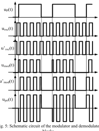
[image:2.595.97.519.55.413.2]The uosc and u’osc are supplied to the two modulators shown in Fig. 4. These devices, wich are also implemented through operational amplifiers and discrete BJT complementary stages, provide the modulated waveforms umod and u’mod, depicted in Fig. 5. As it can be seen, both modulated waveforms have the same shape, but it must be noticed the 180º phase-shift between signals, coming from the oscillator block. Both umod and u’mod signals are supplied to the terminals of the primary side of a transformer, TR1. Therefore, the voltage at the primary of this transformer, upri, has a waveform as depicted in Fig. 5. As it can be seen, this waveform has a negligible DC component, aiming to avoid core saturation for any duty ratio value.
[image:2.595.76.249.352.442.2]At the secondary side, the waveform is rectified by means of fast Schottky diodes and a resistor, to obtain the reconstructed signal urect. Due the effect of parasitic elements at the transformer, at the operational amplifiers and at the BJT stages, this signal might present a slight distortion with respect to the original pulsed signal. This distortion is particularly important in terms of the rising and falling edges of the waveform. In order to ensure fast transitions, the waveform is injected to a comparator and to a final BJT complementary stage, to get the signal ug, that is connected to the gate of the SiC power device.
[image:2.595.331.535.426.695.2]Fig. 3: Schematic circuit of the oscillator block.
Fig. 4: Schematic circuit of the modulator and demodulator blocks.
Fig. 5: Schematic circuit of the modulator and demodulator blocks.
The final power block, shown in Fig. 6, uses the input signals coming from the oscillator in order to generate a pure AC HF waveform, which is supplied to the primary side of a transformer, TR2. At the secondary side, the signal is rectified and filtered, and a regulator provides the reference voltage required to obtain the negative turn off voltage of the driver. This terminal is connected to the source of the power device. Although this approach is indeed a dedicated DC/DC isolated stage, it has advantages versus a conventional power supply. As it is a simple solution, taking benefit of the existing modulating stage, the components count, and as a consequence, the required PCB size is quite small, enabling for better system integration capability. Moreover, the parameters of the voltages can be tuned easily, by adjusting the turns-ratio and the voltage reference, enabling a flexible design for devices with different gate requirements.
Finally, as the transformers in the driver have a custom design, it allows for a full control in the design of the parasitic elements. This enables for keeping under control the parasitic capacitance between primary and secondary sides of the driver, yielding to a high Common-Mode Transient Immunity (CMTI) design of the final driver.
IV. SIMULATION RESULTS
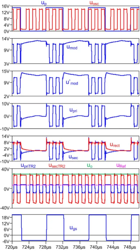
A careful design has been carried out and verified through simulations in an iterative process. The characteristic parameters of the commercial SiC MOSFETs have been used in the implementation play a major role in the system performance. The output turn-on and turn-off VGS values are selected as -5V and +20V, respectively. The modulating signal has been chosen as 500 kHz, the input supply voltage was selected as Vcc=15V and the input PWM signal is TTL compatible. The target switching frequency of the design is 100kHz. Figure 7 shows the main simulation waveforms in the gate driver. As it can be seen, the final output waveform has the required parameters.
V. PROTOTYPE CHARACTERIZATION
Fig. 8 shows the prototype of the proposed gate driver for a single SiC MOSFET. The oscillator, adapting stages and output signal stages have been implemented through discrete OpAmps (LM7171). The power stage have been implemented through complementary transistors. The transformers have been implemented in TX10/6/4 cores from Ferroxcube. It must be noticed that the prototype shown in Fig. 8 can be significantly reduced in size, as it is a single layer design, with relatively large passive components (SMD2106). A size reduction in a factor of 2 to 4 can be easily achieved. The power consumption of the
driver is 3.0W at 100 kHz and 50% duty ratio; a consumption reduction is targeted in future optimizations.
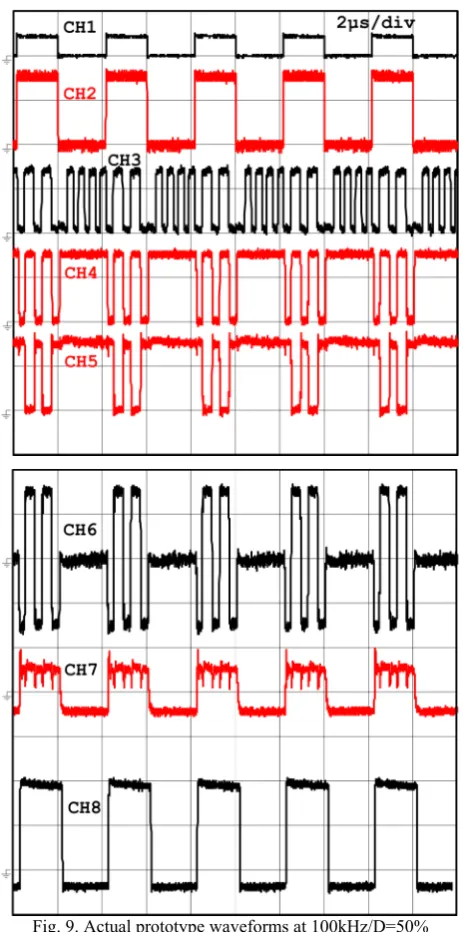
[image:3.595.314.550.170.591.2]The main waveforms in the prototype at 100kHz operation and duty=50% are presented in Fig. 9. CH1 shows the TTL compatible logic signal coming from the control stage. CH2 shows the input signal after an initial step-up stage up to Vcc. CH3 is the signal from the square waveform oscillator. The oscillator is reset at each falling edge of the control signal in order to avoid pulse glitches at the output when both signal pulses are too close.
Fig. 6: Schematic circuit of the secondary side power generation and negative reference block.
Fig. 7: Simulation waveforms of the proposed driver
[image:3.595.88.235.312.410.2]The modulator and adapting stage provides the signals depicted in CH4-CH5. Both signals have the same voltage value (Vcc) at low input voltage, and a complementary modulating signal at high input value. After amplification, each of these signals is connected at the primary transformer terminals, thus the transformer input is directly CH6. At the secondary side, the rectified signal CH7 supplies the output stage (comparator+power stage), to finally provide VGS signal CH8.
The driver has been loaded with different RC circuits that model the gate resistance and capacitance of SiC MOSFETs without drain-source voltage. This is intended to demonstrate the functionality of the design for SiC MOSFETs with different current and voltage ratings in the market. Fig. 10 shows the driver rise and fall times for the given RC combinations (R=0,1,2,5 and 10 Ω, C=0.5, 1, 2 and 4 nF). The driver has been tested at switching frequencies up to 200 kHz, for the full duty range showing good performance.
[image:4.595.324.541.59.334.2]VI. EXPERIMENTAL RESULTS ON A 2 KWCONVERTER The performance of the driver has been tested on an existing 400V/2kW DC-DC buck-boost synchronous converter with C2M0080120D SiC MOSFETs from CREE. Fig. 11 shows the main SiC switches waveforms at 100 kHz, 1.8kW load level.
[image:4.595.46.278.145.612.2]Fig. 9. Actual prototype waveforms at 100kHz/D=50%
Fig. 10: Rise (up) and fall (down) time at the driver output for several R and C values
Fig. 11: Experimental waveforms at a bidirectional buck-boost converter. CH1 (yellow): uGS(t) at Switch S1 (output switch), CH3 (magenta): uDS at S1. CH2 (green): uGS(t) at Switch S2., CH4
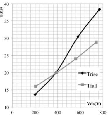
[image:4.595.321.541.435.650.2]Fig 12 shows the details of turn on and turn off. As it can be seen, 38 ns rise time and 27 ns fall time are achieved at 800V drain-source voltage. The gate resistor at the driver has been increased from 0 Ω
up to 15 Ω to reduce the gate ringing that can be seen in Fig. 13. This ringing is due the resonance between the parasitic inductor of the SiC MOSFET and gate driver and the gate capacitance [8]. Fig. 6 shows the VDS rise and fall times vs. the VDS voltage at 100kHz, 50% duty-ratio and 5A output current.
Finally, Figs. 14 and 15 show the power consumption of the proposed modulated driver. Fig 14 shows the power consumption of a single driver, at full load of the converter, at fsw=100kHz and fmod=500kHz, for several duty ratio values. As it can be seen, the power consumption is around 3W. It must be noticed that this value is a minimization target for future versions of the driver. Fig 15 shows the power consumption per driver, at full load of the converter, at fsw=100kHz and D=50%, for several modulating frequencies. As it can be seen, an increase of the modulating frequency would yield to higher power losses in the driver.
VII. CONCLUSIONS
An isolated gate driver for SiC MOSFETs has been proposed, analyzed, built and tested. The prototype shows good general performance in a 2kW buck-boost demonstrator. The proposed driver allows for simple, compact designs of power converters, with full range duty ratio and switching frequencies up to 200 kHz. The main operation principles have been summarized and demonstrated through experimental validation in a working prototype. The main contributions are the ability of the full range duty ratio operation (0%-100%) in SiC devices with asymmetric turn-on/off voltage values in modulated schemes, the absence of blocking capacitor that allows for high bandwidth operation, the synchronization of the HF and LF waveforms to avoid pulse glitches, the implementation of all the scheme through discrete components and operational amplifiers (that allows for full control of the design parameters such as dV/dt, and enables for high size reduction possibilities).
Future developments include optimization in size and consumption of the driver, decreasing of parasitic elements in the
gate-source path in the driver, validation in different WBG devices, inclusion of protections in the driver operation and further optimization of rise and fall time speeds.
REFERENCES
[image:5.595.346.531.95.294.2][1] H. A. Mantooth, M. D. Glover, P. Shepherd, “WBG Technologies and Their Implications on Miniaturizing Power Electronic Systems,” IEEE Jnl. of Em. and Sel. Topics in Power Electronics, vol. 2, no. 3, pp. 374– 385, Sep. 2014.
Fig. 12. VGS (CH1) and VDS (CH2) details at turn on and turn off.
Fig. 13. VDS rise and fall times vs the VDS voltage, for the converter
[image:5.595.58.268.150.356.2]operating at 100kHz, 50% duty-ratio and 5A output current.
Fig. 14. Power consumption per driver, at full load of the converter, at fsw=100kHz and fmod=500kHz, for several duty ratio
[image:5.595.330.538.338.461.2]values.
Fig. 15. Power consumption per driver, at full load of the converter, at fsw=100kHz and D=50%, for several modulating
[image:5.595.327.540.502.633.2][2] H. Chen and D. Divan, “High speed switching issues of high power rated silicon-carbide devices and the mitigation methods,” in 2015 IEEE Energy Conversion Congress and Exposition (ECCE), 2015, pp. 2254– 2260.
[3] H. Qin, B. Zhao, W. Xu, J. Wen, Y. Yan, “Evaluation of performance improvement of SiC MOSFETs based DC-DC converter,” in Power Electronics and Motion Control Conference (IPEMC), 2012, vol. 2, pp. 889–894.
[4] H. J. Ryoo, J. S. Kim, G.H. Rim, D. Sytykh, G. Goussev, "Current loop gate driver circuit for pulsed power supply based on semiconductor switches" 16th IEEE Intl. Pulsed Power Conf., Albuquerque, NM, 2007, pp. 1622-1626.
[5] P.Wood, “Transformer-Isolated HEXFET® Driver provides very large duty cycle ratios”, International Rectifier, Application note 950A.
[6] S. Y. Hui, S. C. Tang and Henry Shu-Hung Chung, "Optimal operation of coreless PCB transformer-isolated gate drive circuits with wide switching frequency range," in IEEE Transactions on Power Electronics, vol. 14, no. 3, pp. 506-514, May 1999 doi: 10.1109/63.761694
[7] T. Bergh, P. Karlsson and M. Alakula, "A resonant galvanically separated power MOSFET/IGBT gate driver," Power Electronics Specialists Conference, 2004. PESC 04. 2004 IEEE 35th Annual, 2004, pp. 3243-3247 Vol.4. doi: 10.1109/PESC.2004.1355355
![[M729.Ebook] Ebook The Courage To Collaborate The Case For Labor Management Partnerships In Education By Ken Futernick.pdf](data:image/gif;base64,R0lGODlhAQABAIAAAP///wAAACH5BAEAAAAALAAAAAABAAEAAAICRAEAOw==)