S. Nireekshan Kumar*, J. Grace Jency Gnannamal**
Abstract — Delay Minimization and Power Minimization are two important objectives in the design of high performance circuits. Retiming is a very effective way of delay optimization of sequential circuits. Bellman ford algorithm is very efficient algorithm used as retiming, but it increases power consumption of the circuit. This paper describes an algorithm in graph theory that finds minimum spanning tree for connected weighted graph. We first discuss the conventional Bellmanford algorithm. Then we discuss DJP Algorithm (Prims algorithm) targeting simultaneous delay and power optimization with compromise. Finally these two algorithms are compared. Experimental results show that Prims algorithm is better than bellman ford algorithm when simultaneous power and delay optimization is needed.
Index Terms – Circuit Optimization, Circuit Synthesis, encoding, Sequential Logic Circuits.
I. INTRODUCTION
Delay minimization and power minimization are two important objectives in the design of the high-performance circuits [1]. Thus, a considerable research effort has been made in trying to find power and delay-efficient solutions to circuit design problems.
In the past, the major concerns of the VLSI designer were area, performance, and cost [2] [3]. Power consumption considerations were mostly of secondary concern. In recent years, however, this trend has begun to change, and, increasingly, power consumption is being given comparable weight to area and speed in VLSI design (Rabaey and Pedram 1996). One reason is that the continuing increase in chip scale integration and the operating frequency has made power consumption a major design issue in VLSI circuits [5]. The excessive power dissipation in integrated circuits not only discourages their use in a portable device, but also causes overheating, which degrades performance and reduces the circuit lifetime. All of these factors drive designers to devote significant resources to reduce the circuit power dissipation. Indeed, the Semiconductor Industry Association identified low-power design as a critical
*Completed Bachelors in Electrical & Electronics Engineering from Madras University in 2004. He is currently Persuing Masters in VLSI Design at Karunya University. His Research Interests are Low Power VLSI, CAD for VLSI and Digital System Design. Phone No: +919940706399; Email: [email protected]
**Completed Bachelors in Electrical & Electronics Engineering from Madras University in 2004. She is currently working as Lecturer in Electronics & Communication Engineering Dept. in Karunya University. Her research interests are CAD for VLSI, VLSI for Communication, Testing. Phone No: +919486073383; Email: [email protected]
technological direction in 1992. There is intense competition of global market and greater demand for high performance circuits even in this era where power consumption is being given comparable weight. Therefore there lies a greater challenge before manufacturers to design a circuit that will have both high performance and Low power consumption. This problem is critical because both are inversely proportional to each other.
Thus, a considerable research effort has been made in trying to find power and delay-efficient solutions to circuit design problems [6] [9]. There are many Procedures for this delay efficient solutions. One such procedure is using bypass transform [7]. Where the unnecessary paths are bypassed. The second method is using exact sensitization [8]. One of most popular method that is applied at the Structural level is architecture retiming [11]. Architecture Retiming is a transformation technique to minimize critical path, there by reducing the delay. Circuit partitioning and floor planning are also methods for finding delay efficient systems. Circuit partitioning aims to divide a given circuit to smaller sub-circuits so that it can be used in the next physical design process for hierarchical design approach. Traditionally, the objective of partitioning is to minimize the amount of interconnection among sub-circuits, which has direct impact on the final chip area. Delay has also been an important objective in partitioning, which aims to minimize the number of inter-partition connection on critical paths. A recent research focused on simultaneous cut size and delay optimization. Another recent study addresses power optimization in clustering. After partitioning the given circuits into sub-circuits, floorplanning is applied to identify the dimension and location of the sub-circuits. Among several ways to perform floorplanning, partitioning based method has been one of the viable approaches. Most partitioning-based floorplanning algorithms attempt to minimize area and wire length. A recent study attempts to minimize wire length and delay in multi-level partitioning based floorplanning.
II. RETIMING
Retiming is a transformation technique used to change the location of delay elements in a circuit without affecting the input/output characteristics of the circuit. Retiming can be used to increase the clock rate of circuit by reducing the computational time of the critical path. Recall that the critical path is defined to be the path with the longest computational time. Among all paths that contain all zero delays, another computation time of the critical path is the lower bound on the clock period of the circuit.
A. Properties of retiming:
The weight of the retimed path p = V0 Æ V1 Æ …..Vk is given by
Wr (p) = W (p) + r (Vk) – r (V0)
1) Retiming does not change the number of delays in a cycle.
2) Retiming does not alter the iteration bound in a DFG as the number of delays in a cycle does not change
3) Adding the constant value j to the retiming value of each node does not alter the number of delays in the edges of the retimed graph.
III. BELLMANFORD ALGORITHM
The Bellman–Ford algorithm, sometimes referred to as the Label Correcting Algorithm, computes single-source shortest paths in a weighted graph (where some of the edge weights may be negative)
Fig 1.1 A sequential Circuit
1. Let M = t max x n, where t max is the maximum
computational time of the nodes in G and n is the number of nodes in G.Since t max = 2 and n=4, then M = 2 X 4 = 8.
2. Form a New Graph Gr which is the same as G except the
edge weights are replaced by wr (e) = M Xw (e) – t (U) for
al edges U to V
Wr (1— 3) = 8 X 1 – 1 = 7
Wr (1— 4) = 8 X 2 – 1 = 15
Wr (3— 2) = 8 X 0 – 2 = -2
Wr (4— 2) = 8 X 0 – 2 = -2
Wr (2— 1) = 8 X 1 – 1 = 7
Fig 1.2 Restructured Sequential Circuit
3. Solve the all-pairs shortest path problem on Gr. Let S’
(U, V) be the shortest path from U to V.
R (0) = inf inf 7 15 7 inf inf inf inf -2 inf inf inf -2 inf inf
R (1) = inf inf 7 15 7 inf 14 22 inf -2 inf inf inf -2 inf inf
R (2) = inf inf 7 15 7 inf 14 22 5 -2 12 20 5 -2 12 20
5 -2 12 20 R (3) = 12 5 7 15 7 12 14 22 5 -2 12 20
S’(U, V) = 12 5 7 15 7 12 14 22 5 -2 12 20 5 -2 12 20
4. To determine W (U, V) & D (U, V), where W(U, V) is the minimum number of registers on any path from node U to node V and D (U, V) is the maximum computation time among all paths from node U to node V with weight W (U, V).
If U = V then W (U, V) = 0 & D (U, V) = t (U).
If U = V then W (U, V) = S’(U, V) / 8 & D (U, V) = M X W (U, V) – S’ (U, V) + t (V)
W (U, V) = 0 1 1 2 1 0 2 3 1 0 0 3 1 0 2 0
D (U, V) = 1 4 3 3 2 1 4 4 4 3 2 6 4 3 6 2
5. The values of W (U, V) & D (U, V) are used to determine if there is a retiming solution that can achieve a desired clock period. Given a clock period ‘c’, there is a feasible retiming solution r such that Phi (Gr) < c if the following constraints hold.
1. (Feasibility constraints) r (U) – r (V) < w (e) for every edge U to V of G.
The Feasibility constraints forces the number of delays on each edge in the retimed graph to be non negative and the critical path constraints enforces Phi (G) < c. if D (U, V) > c then W (U, V) + r (V) – r (U) > 1 must hold for the critical path to have computation time lesser that or equal to c. This leads to critical path constraints.
If c is chosen to be 3, the inequalities r (U) – r(V) < w (e) for every edge U to V are
r (1) – r (3) < 1 r (1) – r (4) < 2 r (2) – r (1) < 1 r (3) – r (2) < 0 r (4) – r (2) < 0
and inequalities r (U) – r (V) < W (U, V) – 1 for all vertices U, V in G such that D (U, V) > 3
r (1) – r (2) < 0 r (2) – r (3) < 1 r (2) – r (4) < 2 r (3) – r (1) < 0 r (3) – r (4) < 2 r (4) – r (1) < 0 r (4) – r (3) < 1
if there is a solution to the 12 inequalities above, then the solution is a feasible retiming solution such that the circuit can be clocked with period c = 3.
The constraint graph is shown below which will not have any negative cycles.
Fig 1.3: Restructured circuit without negative cycles
A. Bellmanford Algorithm for finding shortest path
1. r (1) (U) = 0
2. For K = 1 to n 3. If K = U
4. r (1) (K) = W (U to K) 5. For K =1 to n-2 6. For V = 1 to n
7. r (K+1) (V) = r (K) (V) 8. For W = 1 to n
9. If r (K+1) (V) > r (K) (W) + W (W to V) 10. r (K+1) (V) = r (K) (W) + W (W to V) 11. For V =1 to n
12. For W = 1 to n
13. If r (n-1) (V) > r (n-1) (W) + W (W to V) 14. Return False and exit
15. Return True and exit.
IV. DJP ALGORITHM
DJP algorithm is a n algorithm in graph theory that finds a minimum spanning tree for a connected weighted graph This means it finds a subset of edges that forms a tree that include every vertex, where the total weight of all the edges in a tree is minimized. The algorithm was discovered in 1930 by mathematician vojtech Jarnik and later independently by computer scientist Robert. C. Prim in 1957 and re discovered by Edsger Dijkstra in 1959. Like Kruskal's algorithm, DJP algorithm is based on a generic MST algorithm. The main idea of DJP algorithm is similar to that of Dijkstra's algorithm for finding shortest path in a given graph. Prim's algorithm has the property that the edges in the set A always form a single tree. We begin with some vertex v in
a given graph G =(V, E), defining the initial set of vertices A. Then, in each iteration, we choose a minimum-weight edge (u, v), connecting a vertex v in the set A to the vertex u outside of set A. Then vertex u is brought in to A. This
process is repeated until a spanning tree is formed. Like Kruskal's algorithm, here too, the important fact about MSTs is we always choose the smallest-weight edge joining a vertex inside set A to the one outside the set A.
The implication of this fact is that it adds only edges that are safe for A; therefore when the algorithm terminates, the edges in set A form a MST.
A. DJP algorithm to find the shortest path
DJP (G, w, v) 1. Q ← V[G] 2. for each u in Q do
3. key [u] ← ∞
4. key [r] ← 0
5. π[r] ← NIl
6. while queue is not empty do 7. u← EXTRACT_MIN (Q)
8. for each v in Adj[u] do
9. if v is in Q and w(u, v) < key [v] 10. then π[v] ←w(u, v)
11. key [v] ←w(u, v)
Theorem: DJP algorithm finds a minimum spanning tree. Proof: Let G = (V,E) be a weighted, connected graph. Let
T be the edge set that is grown in DJP algorithm. The proof is by mathematical induction on the number of edges in T and using the MST Lemma.
Basis: The empty set is promising since a connected,
weighted graph always has at least one MST.
Induction Step: Assume that T is promising just before the
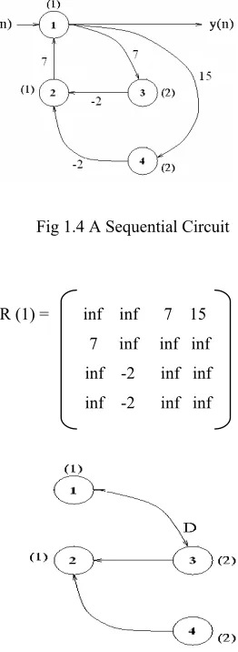
Fig 1.4 A Sequential Circuit
R (1) = inf inf 7 15 7 inf inf inf inf -2 inf inf inf -2 inf inf
Fig 1.5 Retimed sequential circuit
V. SEQUENTIAL BENCHMARK CIRCUIT Sequential benchmark circuits are the circuits which are kept to use for testing the algorithm efficiency. Before they are implemented in hardware. Here in this paper we used ISCAS99 sequential benchmark circuits for testing the algorithm. These benchmark circuits consists of flip-flops, counters etc… The series name of this Benchmark circuits is B series. We used four benchmark circuits namely B01, B02, B03, B04, B05.
VI. EXPERIMENTAL ENVIRONMENT
All experiments were conducted on desktop computer with an Intel Core 2 Duo T5300 CPU (1.73GHz) and 2 GB of RAM. The operating system was Microsoft Windows XP.
VII. RESULTS
Bellman ford algorithm is written in Matlab and converted into VHDL using Accel DSP synthesis tool from Xilinx and then it was tested on ISCAS 99 sequential benchmark circuits. The results are tabulated. DJP algorithm also was written in Matlab and converted into VHDL using Accel Dsp synthesis tool from xilinx and then
it was tested on ISCAS 99 sequential benchmark circuits. The results are tabulated.
The synthesis is done on Xilinx 7.1i. The delay or frequency value is taken from synthesis report. The delay values are represented in terms of nano seconds and frequency values are represented in MHZ. Both the algorithms are compared. The results show that bellman ford algorithm gives high performance than the prims algorithm, but it increases the power dissipation of the circuit. DJP algorithm also give high performance little lesser than bellmanford algorithm, but the power dissipation is reasonable compared to bellmanford algorithm.
[image:4.612.104.235.49.407.2]
Table No-1: Time Values of original Benchmark Circuit
SL
No Benchmark Circuit Original Time
01 B01 2.489 ns 401.99 MHZ
02 B03 1.657 ns 603.300 MHZ
03 B04 9.132 ns 109.505 MHZ
[image:4.612.97.234.49.148.2]04 B05 6.538 ns 152.946 MHZ
Table No-2: Time Values of circuit after applying Bellmanford algorithm
SL No
Benchmark Circuit Time after applying Bellmanford
01 B01 1.103 ns 884.12 MHZ
02 B03 1.102 ns 889.52 MHZ
03 B04 3.203 ns 512.023 MHZ
04 B05 6.538 ns 152.946 MHZ
Table No-3: Time values after applying DJP algorithm
SL
No Benchmark Circuit Time after applying DJP 01 B01 1.930 ns
528.10 MHZ
02 B03 1.382 ns 772.50 MHZ
03 B04 5.489 ns 364.29 MHZ
04 B05 4.023 ns 398.023 MHZ
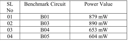
Table No-4: Power Values of original circuit
SL
No Benchmark Circuit Power Value
[image:4.612.316.539.385.498.2]Table No-5: Power Values after applying Bellman ford algorithm
SL
No Benchmark Circuit Power Value
01 B01 879 mW 02 B03 890 mW 03 B04 653 mW 04 B05 604 mW
Table No-6: Power values after applying DJP algorithm
SL No
Benchmark Circuit Power Value
01 B01 674 mW 02 B03 801 mW 03 B04 512 mW 04 B05 580 mW
VIII. CONCLUSIONS
This paper described a graph algorithm which is used as retiming to optimize the delay and power simultaneously with compromise. Since there is always tradeoff between speed and power, both cannot be optimized at a time.
Retiming is a transformation technique which is used to reduce the delay or to reduce power keeping time constant. But if we can make some compromise between power and time values then we can have optimized delay & Power simultaneously.
Table No-1 show the Time period of original Benchmark circuit. Table No-2 show the time period values after applying Bellman ford algorithm, which shows high performance is obtained, but Table No-5 shows that there is drastic increase in the power dissipation values after applying bellmanford algorithm which is not good for any circuit in this low power age.
Table No-3 shows that higher performance is obtained by using DJP algorithm but little lesser than bellmanford algorithm, also Table No-6 shows that power dissipation increase is not much when compared to Table No-5.
Hence it can be concluded that both the delay and power dissipation cannot be optimized simultaneously. But with some compromises made between time & power, simultaneous delay and power optimization is possible. Also we need to search for algorithms which will reduce the delay and power. But we need to make some compromises. DJP algorithm is very useful when we need simultaneous optimization of Delay & Power.
REFERENCES
[1] C.E. Leiserson and J.B. Saxe, “Retiming Synchronous Circuitry,” Algorithmica, Vol. 6, No.1, pp. 5-35, 1991
[2] P. Pan, “Performance-driven integration of retiming and resynthesis,”in Proc. DAC, 1999, pp. 243–246.
[3] Deming and Jason Cong, “A Depth Optimal Area Optimization Mapping Algorithm for FPGA Designs” in Proc. Int. Workshop FPGAs, 1992
[4] E. Lahman, Y. Wantable, J.Grodstein and H. Harkness, “Logic decomposition during technology mapping,” IEEE Trans. Computer-Aided Design integrated circuits & systems vol. 16 n0.8, pp. 813-834, Aug 1997.
[5] Mongkol Ekpanyapong, Karthik Balakrishnan, Vidit Nanda and Sung KyuLim, “Simultaneous Delay and Power Optimization in Global Placement”, in Proc ISCAS 2004.
[6] K. J. Singh, A. R. Wang, R. K. Brayton and A.L. Sangiovanni - Vincentelli, “Timing Optimization of Combinational Logic,” in Proc ICCAD, 1988, pp. 282-285
[7] P.C. McGeer, R.K. Brayton, A.L. Sangiovanni-Vincentelli, and S. K. Sahni, “Performance enhancement through the generalized bypass transform,” in Proc. ICCAD, 1991, pp. 184–187.
[8] A. Saldanha, H. Harkness, P. C. McGeer, R. K. Brayton, and A. L. Sangiovanni-Vincentelli, “Performance optimization using exact sensitization,” in Proc. DAC, 1994, pp. 425–429.
[9] K. J. Singh, “Performance optimization of digital circuits,” Ph.D. dissertation, Univ. California, Berkeley, CA, 1992.
[10] S. Malik, E. M. Sentovich, R. K. Brayton, and A. L. Sangiovanni- Vincentelli, “Retiming and resynthesis: Optimizing sequential networks with combinational techniques,” IEEE Trans. Comput.-Aided Design Integr. CircuitsSys t., vol. 10, no. 1, pp. 74–84, Jan. 1991.
[11] S. Hassoun and C. Ebeling, “Architectural retiming: Pipelining latency constrained circuits,” in Proc. DAC, 1996, pp. 708–713.
[12] for] M.C. V. Marinescu and M. Rinard, “High-level automatic pipelining sequential circuits,” in Proc. ISSS, 2001, pp. 215–220 .
[13] H. Touati, N. Shenoy, and A. L. Sangiovanni-Vincentelli, “Retiming for table-lookup field-programmable gate arrays,” in Proc. Int. Workshop FPGAs, 1992, pp. 89–93.