Quantum capacitance and charge sensing of a superconducting double dot
N. J. Lambert,1,a) A. A. Esmail,1 M. Edwards,1 F. A. Pollock,2, 3 B. W. Lovett,4 and A. J. Ferguson1
1)Microelectronics Group, Cavendish Laboratory, University of Cambridge,
Cambridge, CB3 0HE, UK
2)Atomic & Laser Physics, Clarendon Laboratory, University of Oxford, Parks Road,
Oxford, OX1 3PU, UK
3)School of Physics & Astronomy, Monash University, Clayton, Victoria 3800,
Australia
4)SUPA, School of Physics and Astronomy, University of St Andrews, KY16 9SS,
UK
(Dated: 12 August 2016)
We study the energetics of a superconducting double dot, by measuring both the
quantum capacitance of the device and the response of a nearby charge sensor. We
observe different behaviour for odd and even charge states and describe this with a
model based on the competition between the charging energy and the
superconduct-ing gap. We also find that, at finite temperatures, thermodynamic considerations
have a significant effect on the charge stability diagram.
The ability to make small capacitance devices in which the electrostatic energy per
elec-tron is larger than the thermal energy has allowed a family of ‘single elecelec-tron devices’ to
be made and investigated, including single electron transistors (SETs), semiconductor
dou-ble quantum dots, and superconducting SETs. By using capacitively coupled gate voltages
to manipulate the charge occupancy, they have been exploited as, amongst other things,
charge sensors1–3, probes of chemical potential4, charge qubits5,6 and spin qubits7. The key
to controlling these devices is an understanding of the energetics of the charge states as a
function of the applied gate voltages8.
A superconducting double dot (SDD) comprises two superconducting islands coupled by
a Josephson junction, with each island connected to a normal metal lead by an NIS junction
(Figs 2(a) and 2(b)). It is therefore similar to a semiconductor double dot, but rather
than electrons, the SDD allows electrostatic manipulation of Cooper pairs and Bogoliubov
quasiparticles. In this Letter, we study the charge stability diagram of an SDD. We use
its quantum capacitance to probe the anticrossings between coherently coupled Cooper pair
charge states, and an independent superconducting charge sensor to directly measure the
charge occupancy of the device.
We start by describing the SDD theoretically, following the approaches of Tuominen9
and Lafarge10,11. Its behaviour is governed by the competition between four energy scales:
the superconducting gap (∆), the charging energies of the islands8 (ECR, ECL, ECM), the
temperature (kBT) and the Josephson energy of the middle tunnel junction (EJ). We
calculate the Helmholtz free energy for different charge states of the device, F =U −T S,
whereU is the internal energy of the system andSis the entropy. We label the charge states
(m, n) wherem (n) is the total offset charge from an arbitrarily choseneven parity state on
the left (right) island. For even parity states the ground state is a Cooper pair condensate.
If, however, eitherm orn is odd, then the associated quasiparticle has a momentum degree
of freedom and so the quasiparticle states form a continuous band.
To find the internal energy of the device we solve the Hamiltonian for the system.
Diago-nal elements of the Hamiltonian are given by the sum of the electrostatic energy, UE, which
is found by treating the device as a network of capacitances8, and the energy cost of any
unpaired quasiparticles. States that are related by the transfer of one Cooper pair between
ˆ
H =X
m,n
(UE + ∆(mmod 2 +nmod 2))|m, ni hm, n| −
X m,neven
EJ
2 (|m+ 2, ni hm, n+ 2|+|m, n+ 2i hm+ 2, n|),
(1)
and the Josephson interaction therefore leads to an anticrossing of size EJ between states
coupled by the transfer of a Cooper pair, by analogy with a Cooper pair box13,14.
We now determine the contribution of the entropy to the free energy of quasiparticle
states, following the approach of Tuominen et al9. At low temperatures (k
BT ∆), and in the case where a single quasiparticle is present on an island, the number of microstates
available is given by Neff≈2 √
2πV D(F)
√
∆kBT, where V is the island volume, D() is the
single spin density of states in the normal state and F is the Fermi energy. The entropy is
therefore also parity dependent, and we can now write the free energy of the system as
F(m, n) =UE(m, n) + ˜∆(mmod 2 +n mod 2) (2)
where ˜∆ = ∆−kBT ln(Neff). The free energy of quasiparticle states decreases as
tem-perature increases, with the energy of two-quasiparticle states decreasing at twice the rate
of single-quasiparticle states.
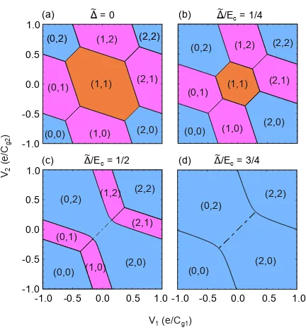
We show the evolution of the calculated charge stability diagram with increasing ˜∆/EC
in Fig. 1, for an ideal device with no cross capacitance between V1(2) and island 2(1). We
use the Ambegaokar-Baratoff relationship between EJ and ∆, EJ = 8e∆2Rmh . For ˜∆/Ec = 0
the stability diagram is that of a metallic double dot (Fig. 1(a)). Increasing ˜∆/Ec has
two effects: the energy cost for quasiparticles increases, leading to charge states with odd
parity reducing in extent (Fig. 1(b)); and an anticrossing opens up between even parity
states. These are analogous to the anticrossings observed in semiconductor double dots15,
and similarly result in a change in∂E/∂Vs, leading to a non-zero quantum capacitance close
to the anticrossing16.
When ˜∆/(Ec−EJ)> 12 then the energy cost of the doubly odd parity (1,1) state is high
enough that it is never the ground state (Fig. 1(c)). Instead, the ground state at V1 = 0,
V2 = 0 becomes the symmetric combination of the Cooper pair states, √12(|2,0i+|0,2i). As
˜
-1.0 -0.5 0.0 0.5 1.0
(0,0) (1,0) (2,0) (0,1) (1,1)
(2,1) (0,2) (1,2) (2,2)
(0,0) (1,0) (2,0) (0,1) (2,1) (0,2) (1,2) (2,2)
V1 (e/Cg1) V2
(e/C
g2
)
-1.0 -0.5 0.0 0.5 1.0 (0,0)
(2,0) (0,2)
(2,2)
-1.0 -0.5 0.0 0.5 1.0 -1.0
-0.5 0.0 0.5 1.0
/Ec = 1/4
~
(0,0) (1,0) (2,0) (0,1) (1,1) (2,1) (0,2) (1,2) (2,2)
~ = 0
~ /Ec = 1/2
~ /Ec = 3/4
(a) (b)
[image:4.612.197.413.67.300.2](c) (d)
FIG. 1. Theoretical charge stability diagrams for (a) ˜∆ = 0, (b) ˜∆ = EC/4, (c) ˜∆ = EC/2 and
(d) ˜∆ = 3EC/2. Blue regions are Cooper pair states, purple regions have one quasiparticle present
and the orange region has one quasiparticle on each island. Dotted lines in (b) and (c) correspond
to anticrossings of the hybridised (2,0) and (0,2) levels.
the stability diagram, and it becomes 2e periodic. At V1 = 0, V2 = 0, the lowest two states
are the symmetric and antisymmetric Cooper pair states which form a two-level system with
energy separation EJ.
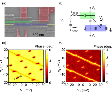
We now present measurements on an SDD. Our device (Figs 2(a), 2(b)) is made using
a standard three angle shadow mask process17. It consists of two Al superconducting
is-lands separated by an Al2O3 tunnel junction formed by in situ oxidation of the Al. They
are connected to normal metal (Al0.98Mn0.02) leads by similarly formed tunnel junctions.
Close to the SDD is a CPB, formed by a superconducting Al island tunnel coupled to a
superconducting Al lead. The two devices are fabricated in one set of depositions, with an
artefact of one of the SDD islands forming the CPB. In order to protect the CPB against
quasiparticle poisoning, it is chosen to be thinner (15 nm) than the lead (25 nm), resulting
in it having a larger superconducting gap18,19, and presenting a barrier to quasiparticles
from the lead20,21. Electrostatic gates are also defined, to allow voltages V
1, V2 and Vc to control the electrochemical potentials of the SDD and CPB. A fourth gate is not used in
(a) (b)
(d) (c)
20
10
0
-10
-20
20
10
0
-10
-20
-30 -20 -10 0 10 20 30 -30 -20 -10 0 10 20 30
Phase (deg.) Phase (deg.)
V1 (mV) V1 (mV)
V2
(mV)
V2
(mV)
LSCDD LCPB
Vrf
V1 V2 Vc
A B
0 2 4 6
[image:5.612.186.423.68.265.2]0 1 2 3 4 500 nm
FIG. 2. The superconducting double dot and Cooper pair box. (a) False colour electron micrograph
of the device. The SDD is shown in blue, the CPB in green, and red regions are the electrostatic
gates. Metallic leads are yellow. Other features are artefacts of the multiple angle evaporation.
(b) Schematic of the experiment. The rf signal is incident on resonant inductorsLSDD and LCPB.
Potentials V1,V2 and Vc are used to control the electrochemical potentials of the SDD and CPB.
(c) Phase response at fSDD as a function of V1 and V2 with Vc grounded, showing the quantum
capacitance of the SDD, and a smaller response due to the quantum capacitance of the CPB. The
line A → B shows the crossection used in Fig. 3. (d) Phase response at fCPB as a function of V1
and V2 withVc grounded. Here the CPB dominates the response, and the signal from the SDD is
reduced.
We measure the complex impedances of the SDD and CPB mounted on the mixing
chamber of a dilution fridge (T = 30 mK) using rf reflectometry. Their leads are bonded
to separate lumped element inductors with resonant frequencies of fCPB = 298 MHz and
fSDD = 350 MHz (Fig. 2(b)), allowing the two components to be probed independently. A
carrier wave of power −105 dBm at one of the two resonant frequencies is incident upon
the resonators, and the reflected power amplified at 4 K and room temperature before being
demodulated to retrieve the phase and amplitude of the reflected signal.
We take care to minimize the nonequilibrium quasiparticle population generated by stray
radiation. The sample is mounted in a light-tight copper box, coated with carbon/carbide
loaded epoxy. We also surround the box with Eccosorb microwave absorbent material.
fridge. The gates are connected to twisted pairs with low-pass (fcutoff = 10 kHz) filters at
30 mK.
The charging energies of the two islands of the SDD are determined from Coulomb
dia-monds to be ≈275µeV. We find the mean value of the superconducting gap for the islands
to be 225µeV. We expect the thinner one to have a larger gap19, but cannot discriminate
between the two islands. The total resistance of the SDD is ≈ 1 MΩ.
In Figs 2(c) and 2(d) we show the phase response for the SDD (2(c)) and CPB (2(d))
as a function of V1 and V2, with Vc grounded. Two sets of features are visible in each case
and we ascribe both to the quantum capacitances of the two devices. The diagonal lines are
due to the quantum capacitance near the charge transitions of the Cooper pair box13 and
the other features are the result of the quantum capacitance of the SDD. We see the same
features in both plots, because the devices are capacitatively coupled; the visibility of the
feature associated with each device is enhanced when that device is probed directly.
In Figs 2(c) and 2(d) we are solely sensitive to the capacitance of the device, and hence see
only the quantum capacitance due to the anticrossings between even parity charge states
mediated by Cooper pair transfer between the islands. Because these anticrossings are
visible, the device must be in one of the two low charging energy regimes shown in Fig. 1(c)
and Fig. 1(d). However, we are not able to infer the presence or otherwise of quasiparticle
states from these measurements.
For the rest of this Letter, we use Vc to compensate for the action of V1 and V2 on the
charge sensor; either to hold it near an operating point (in charge sensing measurements) or
to hold it in a particular charge state, so that charge transitions in the CPB do not affect
the SDD. We first tune the charge sensor away from any transitions, and concentrate on the
response of the resonator coupled directly to the double dot.
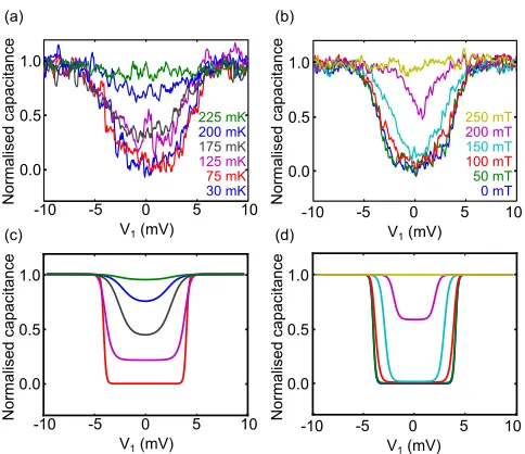
In Fig. 3(a) and 3(b) we show measured phase along the line A → B in Fig. 2(d) as a function of applied in-plane field, B, and temperature. In both cases, the capacitance is
suppressed, as the superconducting gap is decreased. Along with the data in 2(c) and 2(d)
and the doubling of the stability diagram period under large applied fields (B = 2 T), this
suggests that, forB = 0 and our base temperature of 30 mK, the energy scales of our device
are such that ˜∆/(Ec−EJ)> 12, corresponding to the regime shown in either 1(c) or 1(d).
We now use the model described above to calculate the equilibrium thermal occupancy of
temper--10 -5 0 5 10 V1 (mV)
(c) (b) 0 mT 250 mT 200 mT 150 mT 100 mT 50 mT 1.0 0.5 0.0 1.0 0.5 0.0
-10 -5 0 5 10
V1 (mV)
-10 -5 0 5 10
V1 (mV)
(d)
-10 -5 0 5 10
[image:7.612.184.426.68.277.2]V1 (mV) (a) 225 mK 200 mK 125 mK 175 mK 75 mK 30 mK 1.0 0.5 0.0 1.0 0.5 0.0 Norm alised cap acitance Norm alised cap acitance Norm alised cap acitance Norm alised cap acitance
FIG. 3. Quantum capacitance. (a) Normalised device capacitance along A → B in Fig. 2(c) for
increasing temperature. (b) Normalised capacitance along the same line for increasing magnetic
field. In (a) and (b) Vc is used to compensate for the action of V1 and V2, and holds the CPB
in a single charge state. (c) and (d) Calculated normalised device capacitance weighted by state
occupancy for the temperatures (c) and magnetic fields (d) in (a) and (b). In (c), we assume an
base electron temperature of 75 mK, and therefore no curve is plotted for 30 mK.
ature, and hence the expected capacitance signal. We assume a base electron temperature of
75 mK. Two states contribute to the signal. The √1
2(|2,0i+|0,2i) state has positive
quan-tum capacitance, whilst the √1
2(|2,0i − |0,2i) state has negative quantum capacitance of the
same magnitude. This higher lying state is never significantly occupied in our experiments.
The normalised expected signals are plotted in Figs 3(c) and 3(d). Increasing temperature
or increasing magnetic field will suppress ˜∆. However, we see a difference in the dependence
of the quantum capacitance signal on these two parameters; this is due to the increased
thermal occupancy of higher energy states in the case of increasing temperature. Our model
is in qualitative agreement with our measurements. However, because the measurement is
heavily averaged, broadening of the quantum capacitance due to 1/f charge noise from a
background of two level fluctuators is also present in our experimental results, and is not
included in our theory.
Our quamtum capacitance data show we are in one of the two regimes shown in Fig. 1(c)
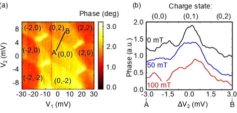
describe charge sensing measurements on the double dot. The charge state of a single
electron device can be measured directly using a charge sensor, which has an impedance
highly sensitive to the local charge distribution. For some charge sensors such as SETs2,3,
the real part of the impedance is measured. Alternatively, charge sensors can rely on a
change to the imaginary part of their impedance, by either a capacitance22 or inductance23
sensitive to the electrostatic environment. This approach offers a way to beat the shot
noise limit for dissipative charge sensors24 and reduces back action on the system to be
measured25,26.
In Fig. 4(a) we show the phase response of LCPBas a function ofV1 andV2. We observe a
hexagonal stability diagram, characteristic of electrostatically coupled double dots, and by
comparing the gate periodicity to the normal state stability diagram measured at B ≈2 T
we find that it is 2e periodic. We also observe here the quantum capacitance of the SDD at
the inter-island charge transitions, as in Fig. 2(d).
In Fig. 4(b) we show the phase along the line A → B in Fig. 4(a) for applied magnetic field values between 0 mT and 100 mT. In this part of the stability digram, the charge sensor
is tuned such that the (0,0) and (0,2) give similar signals in order to maximise the contrast
with the (0,1) state, which is observed between the (0,0) and (0,2) states. This confirms
that we are the regime shown in Fig. 1(c) at B = 0. As B increases, ˜∆ decreases, and the
odd parity (0,1) state increases in size, although most of the stability diagram is still even
parity. At 150 mT and higher, the periodic behaviour of the CPB is suppressed, and it can
no longer act as a charge sensor.
In conclusion, we have theoretically and experimentally studied the charge stability
dia-gram of a superconducting double dot. We find that the behaviour of the SDD depends on
the competition between the charging energies and the gap, and we note that the ground
state of the system can be tailored to include both single and double quasiparticle states.
A device with such states could be used as an electrostatic Cooper pair splitter which, in
contrast to previous work27–29, would retain the split pair. Alternatively, if the splitting is
(a) (b) Phase (deg) 0.0 1.0 2.0 3.0 V2 (mV) 8 4 0 -4 -8
-30 -20 -10 0 10 20 30 V1 (mV)
0.0 0.5 1.0 1.5 2.0 Phase ( a.u.) A B
V2 (mV)
A B
3.0 -1.5
-3.0 0.0 1.5
0 mT 50 mT 100 mT (0,0) (0,2) (0,-2) (-2,0) (-2,-2) (-2,0) (2,0) (2,2)
[image:9.612.187.423.70.183.2](0,0) (0,1) (0,2) Charge state:
FIG. 4. Charge sensing. (a) Phase response at fCPB with Vc acting to hold the CPB close to a
charge transition, andB= 0. A honeycomb charge stability pattern is observed, with a background
phase gradient due to the imperfect compensation of the action ofV1 andV2byVc. (b) Normalised
phase response at fCPB along A→ B, for increasing magnetic fields. As magnetic field increases,
the central plateau corresponding to the (0,1) charge cell enlarges.
ACKNOWLEDGMENTS
We acknowledge support from Hitachi Cambridge Laboratory, and EPSRC Grant No.
EP/K027018/1. A.J.F. is supported by a Hitachi Research fellowship.
REFERENCES
1G. Zimmerli, T. M. Eiles, R. L. Kautz, and J. M. Martinis, Appl. Phys. Lett. 61, 237–239
(1992).
2R. J. Schoelkopf, P. Wahlgren, A. A. Kozhevnikov, P. Delsing, and D. E. Prober, Science
(80-. ). 280, 1238–1242 (1998).
3C. Barthel, M. Kjærgaard, J. Medford, M. Stopa, C. M. Marcus, M. P. Hanson, and A. C.
Gossard, Phys. Rev. B 81, 161308(R) (2010).
4C. Ciccarelli, L. P. Zˆarbo, A. C. Irvine, R. P. Campion, B. L. Gallagher, J. Wunderlich,
T. Jungwirth, and A. J. Ferguson, Appl. Phys. Lett. 101, 122411 (2012).
5Y. Nakamura, Y. A. Pashkin, and J. S. Tsai, Nature 398, 786–788 (1999).
6T. Hayashi, T. Fujisawa, H. Cheong, Y. Jeong, and Y. Hirayama, Phys. Rev. Lett. 91,
226804 (2003).
7J. R. Petta, A. C. Johnson, J. M. Taylor, E. A. Laird, A. Yacoby, M. D. Lukin, C. M.
8W. G. van der Wiel, S. De Franceschi, J. M. Elzerman, T. Fujisawa, S. Tarucha, and L. P.
Kouwenhoven, Rev. Mod. Phys. 75, 1–33 (2002).
9M. T. Tuominen, J. M. Hergenrother, T. S. Tighe, and M. Tinkham, Phys. Rev. Lett.
69, 1997–2000 (1992).
10P. Lafarge, P. Joyez, D. Esteve, C. Urbina, and M. H. Devoret, Nature 365, 422–424
(1993).
11P. Lafarge, P. Joyez, D. Esteve, C. Urbina, and M. H. Devoret, Phys. Rev. Lett. 70,
994–997 (1993).
12K. K. Likharev and A. B. Zorin, J. Low Temp. Phys. 59, 347–382 (1985).
13T. Duty, G. Johansson, K. Bladh, D. Gunnarsson, C. Wilson, and P. Delsing, Phys. Rev.
Lett. 95, 206807 (2005).
14M. A. Sillanp¨a¨a, T. Lehtinen, A. Paila, Y. Makhlin, L. Roschier, and P. J. Hakonen, Phys.
Rev. Lett. 95, 206806 (2005).
15K. D. Petersson, C. G. Smith, D. Anderson, P. Atkinson, G. A. C. Jones, and D. A.
Ritchie, Nano Lett. 10, 2789–93 (2010).
16N. J. Lambert, M. Edwards, A. A. Esmail, F. A. Pollock, S. D. Barrett, B. W. Lovett,
and A. J. Ferguson, Phys. Rev. B 90, 140503 (2014).
17G. J. Dolan, Appl. Phys. Lett. 31, 337 (1977).
18T. Yamamoto, Y. Nakamura, Y. A. Pashkin, O. Astafiev, and J. S. Tsai, Appl. Phys.
Lett. 88, 212509 (2006).
19N. A. Court, A. J. Ferguson, and R. G. Clark, Supercond. Sci. Technol.21, 015013 (2008).
20J. Aumentado, M. Keller, J. Martinis, and M. Devoret, Phys. Rev. Lett. 92, 066802
(2004).
21S. J. MacLeod, S. Kafanov, and J. P. Pekola, Appl. Phys. Lett. 95, 052503 (2009).
22A. C. Betz, R. Wacquez, M. Vinet, X. Jehl, A. L. Saraiva, M. Sanquer, A. J. Ferguson,
and M. F. Gonzalez-Zalba, Nano Lett. 15, 4622–4627 (2015).
23M. A. Sillanp¨a¨a, L. Roschier, and P. J. Hakonen, Phys. Rev. Lett.93, 066805 (2004).
24M. A. Sillanp¨a¨a, L. Roschier, and P. J. Hakonen, Appl. Phys. Lett. 87, 092502 (2005).
25B. Turek, K. Lehnert, A. Clerk, D. Gunnarsson, K. Bladh, P. Delsing, and R. Schoelkopf,
Phys. Rev. B 71, 193304 (2005).
26D. Harbusch, D. Taubert, H. P. Tranitz, W. Wegscheider, and S. Ludwig, Phys. Rev.
27L. Hofstetter, S. Csonka, J. Nyg˚ard, and C. Sch¨onenberger, Nature461, 960–963 (2009).
28L. G. Herrmann, F. Portier, P. Roche, A. L. Yeyati, T. Kontos, and C. Strunk, Phys.
Rev. Lett. 104, 026801 (2010).
29A. Das, Y. Ronen, M. Heiblum, D. Mahalu, A. V. Kretinin, and H. Shtrikman, Nat.