http://dx.doi.org/10.4236/ojm.2012.23004 Published Online August 2012 (http://www.SciRP.org/journal/ojm)
Modelling, Simulation and Optimization of
n-p-n-p
Silicon Multilayer Solar Cells
Abdellatif Bouzidi*, Ahmed S. Bouazzi, Mosbah Amlouk
Unité de Physique des Dispositifs à Semi-Conducteurs, Faculté des Sciences de Tunis, Le Belvédère, Tunis, Tunisia Email: *[email protected]
Received February 10, 2012; revised March 1, 2012; accepted May 9, 2012
ABSTRACT
We simulate the conception parameters of a model of a silicon multilayer solar cell. The cell is composed by four layers of opposite conductivities forming three junctions inside the cell. The electric contacts are tailored vertically to collect the minority carrier generated under illumination. We developed the equations giving the output power, the fill factor and the efficiency of the cell, taking into account the series resistances of each layer. We optimized, using MATLAB software, the thicknesses of the layers, the impurity concentration level and the distance between the electric contacts. We showed that the optimized photovoltaic structure, with the silicon properties published at the Ioffe institute website, gives an efficiency of 20.66%. The n-p-n-p silicon cell delivers a short circuit current Icc = 45.3 mA/cm², an open circuit
voltage Voc = 0.746 V and an output power of 28.5 mW/cm². The corresponding fill factor is FF = 84.29%.
Keywords: Solar Cell; Multilayer; Conception; Optimization
1. Introduction
Nowadays, multilayer solar cells occupy a major place in the field of photovoltaic conversion of solar energy, and they are extensively studied[1-4]. These new structures have the advantage of a better collection of the minority carriers generated by the light near the many depletion regions tailored in series inside the cell, each created electron-hole pair can meet, before recombining, a space charge region near the place where it is created.
Considerable research effort, both theoretically and experimentally, has been made to enhance efficiency of multilayer silicon solar cell. K. Brecl et al. [5] have de-veloped an extended Ebers-Moll model for the examina-tion of the physical parameters of the multilayer cell. They calculate the current-voltage characteristics of floating junction solar cells. They showed that the photocurrent density produced by an n-p-n-pmultilayer solar cell with correspondent layers thicknesses of 0.5 µm, 5.5 µm, 0.4 µm and 30 µm respectively, is equal to 28.19 mA/cm2 using the global AM1.5 solar spectrum.
In a previous work [6], we simulate and optimize the photocurrent densities in a model of an n-p-n-ptype thin film multilayer silicon solar cell for space applications. The equations giving the photocurrent density in each layer of the cell have been developed. We showed that, under the optimum conditions, the n-p-n-p silicon
multi-layer cell delivers a photocurrent density of 46.28 mA/cm2. This density of photocurrent represents the short-circuit current Icc that will be used to simulate the I-V curves.
The optimal thicknesses of the layers define, depending of the impurity concentration, the electrical series resis-tances of the equivalent electric circuit of the multilayer structure.
In another work [7], a new model of multilayer solar cell has been presented; the cell is composed by four layer of opposite conductivity including a frontal layer of n-type 6H-SiC to absorb high energy photons and a back layer of p-type Si0.8Ge0.2 to absorb low energy photons of the solar spectrum. The tow other layers are p-type sili-con layer and n-type silisili-con layer. The optical properties of the semiconductor materials used in this numerical simulation have been taken from the Ioffe institute web-site [8]. We showed that, under the optimum conditions, such optimized multilayer solar cell could deliver a photo- current density of 53.5 mA/cm².
2. Optimization of the n-p-n-p Silicon
Multilayer Solar Cell
After the optimization of the photocurrent densities pro-duced by the multilayer solar cell by optimizing the lay-ers thicknesses [6], we are interesting in the optimization of the output power and the efficiency of the cell.
the cell is taken equal 100 µm for mechanical rigidity. The optimal abscissas were [6]: d1 = 0.1 μm, d11 = 0.2 μm, d2 = 13 μm, d22 = 13.1 μm, d3 = 82 μm and d33 = 82.1 μm.
The optimal photocurrent densities, as shown in Fig-ure 1, are:
Jpd1 = 5.3 mA/cm2, Jnd11 = 23.8 mA/cm2, Jnd2 = 6.9 mA/cm2,
Jpd22 = 5.4 mA/cm2, Jpd3 = 2.2 mA/cm2, and Jnd33 = 0.23 mA/cm2, and the photocurrent densities dues to the space charge regions are:
Jscr1 = 2.4 mA/cm2, Jscr2 = 0.045 mA/cm2 and Jscr3 = 0.003 mA/cm2.
The total photocurrent density produced by the opti-mized n-p-n-p multilayer silicon solar cell is then JTot equal to 46.42 mA/cm2.
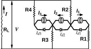
These densities of photocurrent determine the current produced by each junction I1, I2 and I3 in the equivalent electric circuit giving in Figure 2. The abscissas of the layers, with the impurity concentration, give the series electrical resistances R1, R2, R3 and R4.
EV
EF
EC
0 d1 d11 d2 d22 d3 d33 d4
[image:2.595.65.279.343.454.2]n p n p Jnd11 Jpd1 Jnd2 Jpd22 Jnd33 Jpd3
Figure 1. Energy band structure diagram of the multilayer silicon solar cell. The six arrows show the minority carriers path that produces the photocurrent.
I V R3 RL R1 R2 R4
Id2
Id3 Id1
I2
[image:2.595.96.253.508.592.2]I3 I1
Figure 2. The equivalent electric circuit of the multilayer structure. The arrows show the photocurrent created at each junction.
RL is the charge resistance and Id1, Id2 and Id3 are the
diodes current.
The voltage V can be calculated using three ways:
1
1 1 1 1
0
log 1 Id
KT
V R I Id R
q I
2 I1 I2
Id3
2
2 2 1 2 3 2 3 2
0
log 1 Id
KT
V R I I R I I Id
q I
33 4 3 3 2 3
0
log 1 Id
KT
V R I R I I Id Id
q I
2 3
where I0 is the saturation current of the diodes, and is giving by:
0
n p p n
p n
p D n D
I q
L L
Dp and Dn are respectively the diffusion coefficient of
the holes and the electrons; Lp and Ln are respectively the
diffusion length of the holes and electrons; pn and np are
the minority carrier concentration (holes and electrons respectively).
The output voltage of the cell is:
1 2 3
3
V V V
V
The output current is giving by:
1 2 3
1 2 3
I I I I Id Id Id
where:
1 1 1 11
I Jpd Jscr Jnd
2 2 2 22
I Jnd Jscr Jpd
3 3 3 33
I Jpd Jscr Jnd
Id1, Id2 and Id3 are the diodes currents, they depends of the charge resistance RL.
The series resistances of each layer are giving by [9]: 2 1 1 2 n L R d
2 2 2 1 2 p L R d d
2 3 3 2 2 n L R d d
2 4 4 3 2 p L R d d where, n and p are respectively the resistivity of the
n-type layer and the p-type layer. L is the distance be-tween the n-contact and the p-contact (see Figure 3).
We introduced all the developed equations into MATLAB software to simulate under AM0 solar spec-trum the I-V characteristics of the cell. The maximum output power Pmax can be deduced and the efficiency will be giving by:
max 0.136
P
29
19.78%. Many other combinations of layers thickness giving the same value of the efficiency are possible.
Silicon substrate of p++ type
p-Contact
n
p
n
p
n-Contact
d2
d3
d4=100 µm
d1
x
2.2. Optimization of the Impurity Concentration
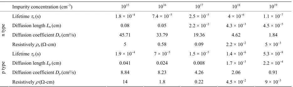
Here we optimize the impurity concentration using the optimal values of layers thicknesses. We simulate, under AM0 solar spectrum and assuming 100 cm/s surface re-combination velocity, the I-V characteristics of the n-p-n-p solar cell for different values of the impurity con- centration going from 105 cm–3 to 1019 cm–3.
[image:3.595.62.288.88.222.2]The electrical properties and the recombination parame-ters, depending of the impurity concentration were taken from Ioffe institute website [7] and given in Table 1. Figure 3. Cross section of the studied n-p-n-p multilayer
silicon solar cell, the light enters from the n-side. We reported in Table 2 the results of simulation cor-responding to the different values of the impurity con-centration.
(Ln, Dn and Lp, Dp). It depends also, of the layers
thick-ness (d1, d2 – d1, d3 – d2 and d4 – d3) in terms of the series resistances, and of the distance L between n-contacts and p-contact. The optimization of the photovoltaic structure supposes three steps:
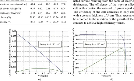
The efficiency of the simulated cells varies from 2.53% for an impurity concentration of 1015 cm–3 to 21.09% for an impurity concentration of 1018 cm3. Figure 5 gives the
I-V characteristic corresponding to an impurity concentration of 105 cm–3 (Figure 5(a)) and 1018 cm–3 (Figure 5(b)).
1) Optimization of the layers thickness; 2) Optimization of the impurity concentration; 3) Optimization of the distance between contacts.
2.1. Optimization of Layers Thicknesses
We begin by optimizing the layers thicknesses defined by the abscissas d1, d2, d3 and d4. We computed the efficiency of the n-p-n-p silicon solar cell by varying all the abscissas in a three dimensional space d1, d2 and d3. The abscissa d4 is fixed equal to 100 µm which represents the total cell thick-ness. The impurity concentration is taken equals 1017 cm–3 in all the photovoltaic structure to ensure. As an illustration, Figure 4 gives the efficiency of the n-p-n-p solar cell versus the first and the second layer abscissa.
We can see that the efficiency of the cell decreases when d1 and d2 increases.
The program of simulation written in MATLAB gives the three optimal abscissas and the maximum efficiency
under the prefixed simulation conditions: Figure 4. Efficiency of theand the second layer abscissa. The third layer abscissa n-p-n-p solar cell versus the first d3 is taken equal to 60 µm.
[image:3.595.310.534.361.531.2]d1opt = 4 µm, d2opt = 10 µm, d3opt = 45 µm and max =
Table 1. Recombination parameters versus impurity concentration.
Impurity concentration (cm3) 1015 1016 1017 1018 1019
Lifetime n (s) 1.8 × 10⁴ 7.4 × 10⁵ 2.5 × 10⁵ 4 × 10⁶ 1.1 × 10⁷
Diffusion length Ln (cm) 0.08 0.05 2.2 × 10² 4.3 × 10³ 4.5 × 10⁵
Diffusion coefficient Dn (cm²/s) 45.71 33.79 19.36 4.62 1.84
n type
Resistively n (-cm) 5 0.58 0.09 2.2 × 10² 5 × 10³
Lifetime p (s) 1.9 × 10⁴ 7 × 10⁵ 1.5 × 10⁵ 1.4 × 10⁶ 5.3 × 10⁸
Diffusion length Lp (cm) 0.041 0.024 0.008 1.7 × 10³ 2.2 × 10⁴
Diffusion coefficient Dp (cm²/s) 8.84 8.23 4.26 2.06 0.91
p type
[image:3.595.68.535.598.737.2]The efficiency of the n-p-n-p silicon multilayer solar cell corresponding to an impurity concentration of 105 cm3 is too week (less then 3%). This is due to the lack of minority carriers to be generated under illumination.
The efficiency of the cell decreases with an impurity concentration of 1019 cm–3 and it doesn’t exceed 17%. This low efficiency is due to the high recombination pos-sibility and the important values of layers resistances, which depends on the minority carriers electrical proper-ties as giving above.
We can see from Table 2 that the maximum efficiency is obtained with an impurity concentration of 1018 cm–3. Thus, the optimal concentration is in proximity of 1018 cm–3. We computed our simulation using an impurity concentration level between 3 × 1017 cm–3 and 5 × 1018 cm–3. The optimal impurity concentration is obtained equals to 1018 cm–3.
2.3. Optimization of the Distance between Electric Contacts
[image:4.595.67.507.454.720.2]In all our previous simulation we considered that the electric contact thickness is negligible and that there are no losses of light absorption at the front surface of the cell. In reality, this is not totally true. In fact, the surface of the electric contacts tailored inside the cell causes a significant loss of light absorption under illumination. Consider that the contact thickness is Scontact equal to 5
Table 2. Results of impurity concentration optimization.
Impurity concentration (cm3) 1015 1016 1017 1018 1019 Short-circuit current (mA/cm²) 47.4 46.6 46.3 46.0 37.0
Open circuit voltage (V) 0.35 0.62 0.68 0.75 0.74
Output power (mW/cm²) 3.40 23.7 26.9 28.7 22.6
Fill factor (%) 20.83 82.86 84.27 83.36 82.56
Efficiency (%) 2.53 17.44 19.75 21.09 16.61
µm, which is a realistic value, and that the number of contacts per square centimetre is k equal to 15. The re-maining illuminated surface of the cell will be:
2
remaining(cm ) 1 contact 0.9925
S k S
The flux of light received by the photovoltaic cell is:
received total 1 k Scontact
We computed our MATLAB program taking in ac-count the received quantum of incident photon energy, and we simulate the efficiency of the n-p-n-p silicon multilayer solar cell for different values of the contact thickness. The program of simulation gives the optimal number of contacts and the optimal distance between contacts giving the maximum efficiency for each value contact thickness.
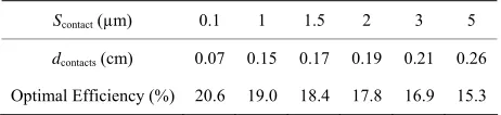
We use the optimal layers thicknesses obtained in 2.1 and the optimal impurity concentration obtained in 2.2. Figure 6 gives the simulated efficiency versus the con-tact thickness and the distance between concon-tacts.
We can see from the three dimensional curve, that for each contact thickness correspond an optimal distance between contacts which gives the maximum efficiency of the cell. Table 3 resumes the optimal distance between contacts (dcontacts) and the maximum efficiency obtained with some choosing values of the contact thickness Scon-tact.
The efficiency of the conceived multilayer solar cell decreases when the thickness of the electric contacts in-creases. This efficiency drop is due to the non-illumi- nated surface resulting from the some of electric contact thicknesses. The efficiency of the n-p-n-p silicon solar cell, with a contact thickness of 0.1 µm is equal to 20.6%. The efficiency of the cell decreases to only about 15% with a contact thickness of 5 µm. Thus, special care may be accorded to the insertion or the growth of the electric contacts to achieve high efficiency values.
(a) (b)
31
Figure 6. Efficiency versus contact thickness and distance
efficiency and distance between contacts
2 3 5
between contacts.
able 3. Optimal T
for different values of contacts surface.
Scontact (µm) 0.1 1 1.5
dcontacts(cm) 0.07 0. 15 0.17 190. 0.21 0.26
Optimal Efficiency(%) 20.6 19.0 18.4 17.8 16.9 15.3
3. Conclusions
ized the conception parameters of a
er;
: 1018 cm–3;
.
gi cell
de
sq
re grateful an anonymous referee for helpful com-k Kim Humphreys for
Eng-B. Rezig, “A New Model of Very High Efficiency Buried Emitter Silicon Solar Cell,”
Solar Energy ls, Vol. 46, No. 1,
In this work we optim
proposed n-p-n-p multilayer solar cell composed by four layers of opposite conductivities forming three junctions inside the cell. The electric contacts are tailored verti-cally to collect the minority carrier generated under illu-mination.
The optimization of the cell conception was accom-plished within three steps: optimization of the layers thicknesses, optimization of the impurity concentration and optimization of the distance between electric con-tacts. The optimization of the layers thicknesses takes into account the series resistances of each layer which determine the voltage drop inside the cell.
The optimization of the impurity concentration is based on the research of the best compromise between lacks and exceeds of electric carrier to be generated un-der illumination. Finally the distance between electric contacts was optimized tacking into account the non- illuminated surface due to the contact thicknesses.
The optimal parameters are: Optimal layers abscissas:
r; d1 = 4 µm for the first laye d2 = 10 µm for the second lay d3 = 45 µm for the third one; The optimal impurity concentration
The optimal electric contact thickness: 0.1 µm; The optimal distance between contacts: 0.07 cm The optimized photovoltaic structure, with the silicon
properties published at the Ioffe institute website [Ioffe], ves an efficiency of 20.66%. The n-p-n-p silicon
liver a short circuit current Icc= 45.3 mA/cm², an open
circuit voltage Voc= 0.746 V and an output power of 28.5
mW/cm². The corresponding fill factor is FF = 84.29%. These values of the cell performances can be improved by using a best quality of silicon like those used by M. Green in PERC and PERL cells [10] and by using a
uare based pyramids surface in the front face of the cell.
4. Acknowledgements
We a
ments. We also wish to than lish editing. All errors are ours.
REFERENCES
[1] A. S. Bouazzi, M. Abaab and
Material and Solar Cel
1997, pp. 29-41. doi:10.1016/S0927-0248(96)00091-8 [2] J. Krc, K. Brecl, F. Smole and M. Topic, “The Effects of
Enhanced Light Trapping in Tandem Micromorph Silicon Solar Cells,” Solar Energy Materials and Solar Cells, Vol.
90, No. 18-19, 2006, pp. 3339-3344.
[3] J. Kwak, S. Won Kwon and K. S. Lim, “Fabrication of a n-p-p Tunnel Junction for a Protocrystalline Silicon Mul-tilayer/Amorphous Silicon Tandem Solar Cell,” Journal of Non-Crystalline Solids, Vol. 352, No. 9-20, 2006, pp.
1847-1850.
[4] R. R. Arya, “Amorphous Silicon Based Solar Cell Tech-nologies: Status, Challenges, and Opportunities,” Materi-als Research Society Symposium Proceedings, Vol. 808
2011, 11 pages. doi:10.1557/PROC-808-A7.5
[5] K. Brecl, F. Smole and J. Furlan, “Modelling of Multi-layer Thin-Film Solar Cells,” Progress in Photovoltaics: Research and Applications, Vol. 7, No. 6, 1999, pp. 449-
456.
doi:10.1002/(SICI)1099-159X(199911/12)7:6<449::AID-PIP286>3.0.CO;2-U
[6] A. Bouzidi, A. S. Bouazzi and B. Rezig, “Photocurrent Density Simulation in an n-p-n-p Silicon Multilayer Solar Cell,” The European Physical Journal Applied Physics,
Vol. 31, No. 1, 2005, pp. 11-16. doi:10.1051/epjap:2005036
[7] A. Bouzidi, H. Hamzaoui, A. S. Bouazzi and B. Rezig, “Analytic Computation of the Photocurrent Density in a n-6H-SiC/p-Si/n-Si/p-Si0.8Ge0. Multilayer Solar Cell,”
croelectronics Journal, Vol. 32
Mi-
7, No. 5, 2006, pp. 388-394. doi:10.1016/j.mejo.2005.06.011
[8] Ioffe Physical Technical Institute, 2012. http://www.ioffe.ru
[9] A. S. Bouazzi, M. Abaab and B. Rezig, “The Effect of the ics of a Silicon
ic Solar Energy
[image:5.595.57.288.320.373.2]Conference, Barcelona, 30 June-4 July 1997. Vol. 65, No.
[10] M. A. Green and S. R. Wenham, “Novel Parallel
Multi-junction Solar Cell,” Applied Physics Letters,