Active Thermal Sensor for Improved Distributed Temperature Sensing in
Haptic Arrays
D Cheneler1, MCL Ward2
1
Department of Engineering, Lancaster University, Lancaster, UK
2 School of Engineering and the Built Environment, Birmingham City University, Birmingham, UK
Correspondence should be addressed to David Cheneler; [email protected]
The efficacy of integrating temperature sensors into compliant pressure sensing technologies, such as haptic sensing arrays, is limited by thermal losses into the substrate. A solution is proposed here whereby an active heat sink is incorporated into the sensor to mitigate these losses, whilst still permitting the use of common VLSI manufacturing methods and materials to be used in the sensors fabrication. This active sink is capable of responding to unknown fluctuations in external temperature, i.e. the temperature that is to be measured, and directly compensates in real-time for the thermal power loss into the substrate by supplying an equivalent amount of power back into the thermal sensor. In this paper, the thermoelectric effects of the active heatsink/thermal sensor system are described and used to reduce the complexity of the system to a simple one-dimensional numerical model. This model is incorporated into a feedback system used to control the active heat sink and monitor the sensor output. A fabrication strategy is also described to show how such a technology can be incorporated into a common bonded silicon-on-insulator (BSOI) based capacitive pressure sensor array such as that used in some haptic sensing systems.
1. Introduction
There are many variants of silicon-based sensors available today [1-3]. Many of the compliant sensors, in particular strain and pressure sensors, require temperature compensation in order to mitigate thermal expansion effects [2]. As such, many designs incorporate some manner of structure to prevent/correct for thermal expansion [4] or some manner of temperature sensor, usually a temperature sensitive resistor, to facilitate correction of the sensor output [5, 6]. In general, these integrated temperature sensors do not provide a measure of the actual ambient temperature, but rather the temperature of the compliant sensor, which is a function of not only of the ambient temperature but also of thermal losses through the substrate. However, there are several instances where one is interested in the temperature not to simply correct other sensors, but to provide an additional sensing modality. A typical scenario where this applies is with haptic arrays where one may wish to incorporate an array, sometimes hundreds, of compliant pressure sensors into some manner of robotic end effector to monitor contact and facilitate the handling of objects [6-9]. Temperature sensors are often incorporated into these arrays to provide a more biomimetic sensing modality [10-11].
varies linearly with temperature, although the self-heating effects need to be considered [16]. However, if every pressure sensor in a large haptic array requires individual conventional temperature sensors or a commercial RTD located next to it, then the spatial resolution of the tactile sensor will be severely undermined. By integrating a micro thermal sensor into the same substrate as the pressure sensor, the temperature dependent error of the pressure sensor can be minimised without dramatically affecting the resolution of the array and still allow an accurate measurement of the ambient temperature. Using existing designs, such a sensor, however, will be very sensitive to its environment, in particular the substrate, due to the previously mentioned thermal losses.
This paper aims to address this issue through the incorporation of a micro active heat sink that acts as an intermediate structure between the thermal sensor and the substrate. The system is designed to be suspended away from the substrate in a similar manner to many silicon-based pressure sensors, especially capacitive diaphragm based sensors [17-19], so that it can be fabricated in much the same way. The fabrication method is detailed below. Both the thermal sensor and active sink are thermoelectric elements that are sensitive to the thermal energy that flows in and out of the respective elements, however, the active sink actively responds to losses from the sensor into the substrate and compensates accordingly by providing the equivalent power back to the sensor in real-time. This allows the thermal sensor to behave as though it is thermally isolated from the substrate below, ensuring its output is only a function of the external ambient temperature/heat flux. The system is analytically and numerically modelled below to elucidate its thermodynamic behaviour and to justify simplified one-dimensional expressions that are then used in the feedback system. This feedback system is used to control the output of the active heat sink automatically and monitor the thermal sensor output.
2. Basic Design
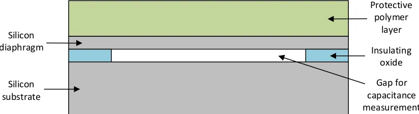
[image:2.595.92.504.621.734.2]The pressure sensors used in a tactile array are often diaphragm based capacitive sensors [17-21] whereby the external contact force deflects the diaphragm changing the gap between it and the substrate, resulting in a change in capacitance between the two. A typical silicon based design is shown in Fig. 1. While many equivalent designs are possible, for simplicity it is assumed here that the pressure sensor was fabricated on a bonded silicon-on-insulator (BSOI) wafer coated with a polymer layer for protection with the diaphragm being released through selective etching of the insulating oxide layer. The theory that follows is applicable for many, not necessarily silicon-based, equivalent designs, provided that the sensor consists of two conductive elements (the diaphragm and substrate) separated by an electrically, but not thermally, insulting layer (the oxide layer in this example).
Fig. 1: A schematic of a typical capacitive pressure sensor (not to scale).
Protective polymer
layer
Insulating oxide
Gap for capacitance measurement Silicon
diaphragm
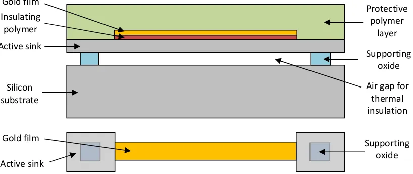
The thermal sensor would need to be as close as possible to the pressure sensor in order to reduce the size of the array and to make accurate measurements without introducing too many additional fabrication steps. Therefore, the thermal sensor will ideally be fabricated on the same layer as the silicon diaphragm. However, a simple temperature sensor comprising of a thin wire of silicon etched out of the device layer of the BSOI will not suffice. This is due to the high thermal conductivity of both silicon and its oxide. If the silicon substrate is maintained at room temperature, any heat energy supplied through the polymer layer will be lost immediately to the substrate and the temperature sensor will not work as intended. A heating element at the same temperature as the ambient temperature located between the sensor and the substrate would mean the temperature gradient across the sensor would be zero and no heat will be lost. This can be achieved if the sensor is fabricated on top of an ‘active sink’. Both the sensor and the active sink will be maintained at a constant, slightly elevated, temperature by monitoring their resistance and controlling the voltage passing through them so that their resistance is maintained at a predefined value. A schematic of a typical temperature sensor is shown in Fig. 2.
Fig. 2: A schematic of a temperature sensor with active sink. The gold film acts as the sensing element. Top: a cross-sectional view showing the different layers. Bottom: a top view without
protective polymer layer and substrate.
This schematic is the simplest configuration of the active sink design. In practice, one would wish the thermal sensor and its sink to be much stiffer than the pressure sensor to avoid contact with the substrate whilst under load. This can be achieved by making the sensor short. This will reduce the resistance and so one may wish to have several of these elements acting together like a long thermal sensor with higher resistance supported by several intermediate islands of oxide. These designs are all equivalent and the theory below applies to them all.
3. Theory
It has been known for a long time that the passage of an electric current through a conductor releases heat. The phenomena was first studied by James Joule in 1841 [22] and the equation for the temperature in a thin wire through which a constant current is flowing was found by Verdet in 1872 [23]. It was discovered that the mechanisms behind both electrical and thermal conduction were inextricably linked. It is now known that Joule heating, or resistive heating is caused by interactions between the moving current and the charged atoms that make up the body of the conductor. Charged particles in the electric circuit are accelerated by an electric field but give up some of their kinetic energy each time they collide
Protective polymer
layer
Supporting oxide
Air gap for thermal insulation Active sink
Silicon substrate Insulating polymer Gold film
Supporting oxide Active sink
with an ion. The increase in the kinetic or vibrational energy of the ions manifests itself as heat and a rise in the temperature of the conductor. Hence, energy is transferred from electrical power to the conductor and any materials with which it is in thermal contact [24]. This transfer of energy though molecular interaction is very similar to that accomplished through heat conduction, except in this case the motion is not necessarily caused by an electric field but through momentum exchange from a molecule with a higher energy level [25].
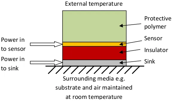
[image:4.595.148.437.213.386.2]In general, this is a three dimensional thermo-electric problem. However, as will be shown, the problem reduces to a simpler one dimensional problem. The schematic for the simplified model is shown below:
Fig. 3: A schematic of the one-dimensional representation of the temperature sensor with active sink. The temperature variation will be in the vertical direction.
As can be seen in Fig. 3, the device can be considered to be a simple layered structure. The top layer, the protective polymer, is an insulating layer between a surface set at the external temperature and a surface at the temperature of the sensor. The sensor is a highly conductive thin layer which has a current flowing through it. There is heat energy being generated within the sensor due to electrical resistance and energy exchange through the polymer and insulator layers. The insulating layer is similar in nature to the polymer layer except the external temperatures are dictated by the temperature of the sensor and active sink respectively. The active sink is another highly conductive thin layer with a current flowing through it. Again heat energy is generated due to the electrical resistance and energy is exchanged through the insulation layer. However, an additional complication is that energy is also lost from the ends of the sink through the oxide as well as from the surrounding air.
The method for solving this problem was to treat the four layers as four coupled partial differential equations, which could then be solved numerically. The governing differential equation for a one dimensional transient conduction problem with internal energy generation is given by [26]:
(1) 𝑘𝜕2𝑇
𝜕𝑥2+ 𝑞̇ = 𝜌𝐶𝑝
𝜕𝑇 𝜕𝑡
Where 𝑘 is the thermal conductivity of the layer in 𝑊/(𝑚. 𝐾), 𝑇 is the temperature distribution within the layer in 𝐾, 𝑞̇ is the rate of heat energy generated within the layer per unit volume, 𝜌 is the density in 𝑘𝑔/𝑚3 and 𝐶𝑝 is the specific heat of the material in 𝐽/(𝑘𝑔. 𝐾). This essentially means, considering
just a small element of material within the layer:
Surrounding media e.g. substrate and air maintained
at room temperature Power in
to sensor Power in to sink
Protective polymer
Sensor
Insulator
(2) {
𝑅𝑎𝑡𝑒 𝑜𝑓 𝑒𝑛𝑒𝑟𝑔𝑦 𝑐𝑜𝑛𝑑𝑢𝑐𝑡𝑖𝑜𝑛 𝑖𝑛𝑡𝑜
𝑒𝑙𝑒𝑚𝑒𝑛𝑡
} − {
𝑅𝑎𝑡𝑒 𝑜𝑓 𝑒𝑛𝑒𝑟𝑔𝑦 𝑐𝑜𝑛𝑑𝑢𝑐𝑡𝑖𝑜𝑛 𝑜𝑢𝑡
𝑜𝑓 𝑒𝑙𝑒𝑚𝑒𝑛𝑡 } + {
𝑅𝑎𝑡𝑒 𝑜𝑓 𝑒𝑛𝑒𝑟𝑔𝑦 𝑔𝑒𝑛𝑒𝑟𝑎𝑡𝑖𝑜𝑛 𝑤𝑖𝑡ℎ𝑖𝑛 𝑒𝑙𝑒𝑚𝑒𝑛𝑡
} = {
𝑅𝑎𝑡𝑒 𝑜𝑓 𝑎𝑐𝑐𝑢𝑚𝑢 − 𝑙𝑎𝑡𝑖𝑜𝑛 𝑜𝑓 𝑒𝑛𝑒𝑟𝑔𝑦
𝑤𝑖𝑡ℎ𝑖𝑛 𝑒𝑙𝑒𝑚𝑒𝑛𝑡 }
In the protective polymer layer there is no internal heat generation and the temperature gradient within is completely determined by its initial temperature distribution and boundary conditions. The initial temperature distribution is assumed to be constant and at room temperature as will be the case before the device is turned on and any changes to the external temperatures have been made. The boundary conditions are the temperatures of the outer surface and of the sensor. Given this, the differential equation governing this layer is:
(3) 𝜕𝑇
𝜕𝑡 = 𝛼 𝜕2𝑇
𝜕𝑥2
where 𝛼 = 𝑘/𝜌𝐶𝑝 and is known as the thermal diffusivity and is expressed in 𝑚2/𝑠. This equation is
known as Fick’s second law and is essentially the diffusion equation [25]. Analytical solutions exist for this equation as shown in Appendix A, however numerical integration of the highly oscillatory integrals found in the solution mean that the solution required extensive computation time and so is not very convenient for further numerical analysis. It is far more convenient in this case to solve eq. 3 fully numerically using the Crank-Nicolson method as described in Appendix B [27]. The solution for the transient temperature distribution for the insulation layer is found in exactly the same way, with the end temperatures set by the temperature of the active sink and sensor respectively.
The sensor has a high thermal conductivity and is very thin compared to the surrounding materials. This means that it can be assumed that the temperature at any instant is effectively constant throughout the layer. In this case, the layer is known as being “thermally thin” [28]. From eq. 2 it can be seen that the governing equation becomes:
(4) 𝜌𝐶𝑝𝑣 𝜕𝑇
𝜕𝑡= 𝑞̇𝑖𝑛− 𝑞̇𝑝+ 𝑞̇𝑣
where 𝑣 is the volume of the layer, 𝑞̇𝑖𝑛 is the energy entering via the insulator and 𝑞̇𝑝 is the energy
being dissipated through the polymer layer. Naturally the signs of 𝑞̇𝑖𝑛 and 𝑞̇𝑝 depend on the
instantaneous temperature distributions within the respective layers and so may change. The energy exchange, 𝑞̇𝑖, through the relevant layers is due to conduction which is described by the Fourier rate
equation:
(5) 𝑞̇𝑖 = 𝑘𝐴 𝜕𝑇 𝜕𝑥
where 𝐴 is the area of the layer in thermal contact with the other layer. The rate of generation of heat due to electrical resistance in a conductor can be calculated by Ohm’s law:
(6) 𝑃 = 𝑞̇𝑣 = 𝑉𝐼 = 𝑉2
𝑅
where 𝑃 is power in watts, 𝑉is the voltage across the sensor, 𝐼 and 𝑅 is the current through and the resistance of the sensor respectively. As no other work is being done, all the energy generated as electrical power is dissipated as heat. It is assumed that the resistance will be linearly dependent on temperature as shown in eq. 7. This assumption is reasonable over small ranges of temperature.
(7) 𝑅 = 𝜌𝑒𝐿
where 𝜌𝑒 is the initial resistivity of the sensor at room temperature measured in Ω 𝑚, 𝐿 is the length of
the conductor in 𝑚, 𝐴𝑐 is its cross-sectional area in 𝑚2, 𝑎 is the temperature coefficient of resistance
for the layer measured in 1/𝐾 and ∆𝑇 is the change in temperature of the layer from room temperature. Therefore the equation to solve for the response of the sensor can be shown to be:
(8) 𝜕𝑇
𝜕𝑡 = 1 𝜌𝐶𝑝𝑣[(𝑘𝐴
𝜕𝑇
𝜕𝑥)𝑖𝑛− (𝑘𝐴 𝜕𝑇 𝜕𝑥)𝑝+
𝑉2
𝜌𝑒𝐿 𝐴𝑐(1+𝑎∆𝑇)
𝑣]
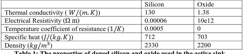
[image:6.595.168.442.383.514.2]As was mentioned above the active sink behaves in a manner similar to the sensor. This means the governing equation for the sink is the same as eq. 4. It is also assumed that the heat exchange to the insulation layer and to the air is of the same form as eq. 5 and that the resistance of the sink varies in the same manner as eq. 7. The difference lies in the exchange of heat to the substrate. Whereas the sensor is in complete thermal contact along its length with the polymer and insulator layer, the active sink is only in contact to the substrate at the ends. This was deliberate in order to reduce the amount of heat loss from the sink. The consequence of this decision is that there is a temperature distribution along the length of the sink. For example, consider an active sink comprised of silicon, with a potential of 1V is applied across it, of dimensions 1000×100×2 μm connected to a substrate maintained at room temperature via silicon blocks of 150×150×2 μm on top of silicon dioxide blocks of 50×50×2 μm as shown in Fig. 4. The silicon was assumed to be doped to saturation with arsenic to make it electrically conductive. The properties of the silicon and its oxide are given in Table 1.
Fig. 4: The steady state temperature distribution of the active sink when 1V is applied across it, as found using FEA in Comsol.
Silicon Oxide
Thermal conductivity ( 𝑊/(𝑚. 𝐾)) 130 1.38
Electrical Resistivity (Ω m) 0.00006 10e12
Temperature coefficient of resistance (1/𝐾) 0.0005 0
Specific heat (𝐽/(𝑘𝑔. 𝐾)) 712 703
Density (𝑘𝑔/𝑚3) 2330 2200
Table 1: The properties of doped silicon and oxide used in the active sink
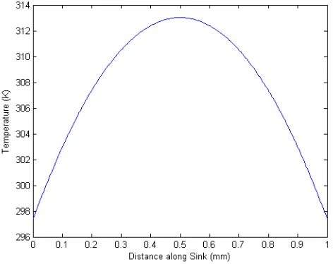
As can be seen in Fig. 4, the thermo-electric problem for the active sink has been solved using Comsol 4.3, a commercial FEA package [29]. The results show that there is a temperature distribution along the length of the sink in a direction perpendicular to the assumed direction of heat flow as dictated in Fig. 3. This is because the dominant heat loss mechanism in the active sink is conduction through the ends of the sink to the substrate below, which is maintained at room temperature. In order to reduce this problem to the required equivalent one-dimensional problem, it is necessary to ensure that the relevant heat exchange mechanisms are the same for both cases. Plotting the steady-state temperature
Max: 313.03 K
[image:6.595.104.502.555.643.2]distribution for the active sink in a more convenient form, see Fig. 5, shows that the temperature distribution is essentially parabolic in nature. This means the temperature distribution can be assumed to have the form:
(9) 𝑑𝑇𝑑(𝑦) = 𝑑𝑇0[1 + 4 ( 𝑦 𝐿−
1 2)
2
] + 𝑑𝑇𝑒𝑛𝑑
where 𝑑𝑇𝑑(𝑦) is the horizontal temperature distribution in the horizontal direction, 𝑦, along the length,
𝐿, of the active sink. 𝑑𝑇𝑒𝑛𝑑 is the difference between the temperature of the ends of the sink and room
[image:7.595.175.411.228.415.2]temperature and 𝑑𝑇0 is the difference between the peak temperature in the sink and 𝑇𝑒𝑛𝑑.
Fig. 5: The one-dimensional steady state temperature distribution of the active sink when 1 V is applied across it, as found using Comsol. Note room temperature was set to 293 K. In order to be consistent, the energy converted from electrical to heat needs to be the same in the two-dimensional and the one-two-dimensional case. The electrical power passing through the sink is given by combining eqtns. 6 and 7. In the one-dimensional case it is assumed that the temperature difference is constant throughout the sink, i.e: ∆𝑇 = 𝑑𝑇𝑐, and so the power can be given as:
(10) 𝑃 = 𝐼2 𝜌𝑒𝐿
𝐴𝑐 (1 + 𝑎 𝑑𝑇𝑐)
In the two-dimensional case, the temperature distribution has to be taken into account. In this situation the power can be expressed as:
(11) 𝑃 = ∫ 𝐼2 𝜌𝑒𝐿
𝐴𝑐 (1 + 𝑎 (𝑑𝑇0[1 + 4 (
𝑦 𝐿−
1 2)
2
] + 𝑑𝑇𝑒𝑛𝑑)) 𝐿
0 𝑑𝑦
Eq. 11 can be solved to give:
(12) 𝑃 = 𝐼2 𝜌𝑒𝐿
𝐴𝑐 (1 + 𝑎 [ 2
3𝑑𝑇0+ 𝑑𝑇𝑒𝑛𝑑])
(13) 𝑑𝑇𝑐 = 2
3𝑑𝑇0+ 𝑑𝑇𝑒𝑛𝑑
However in assuming that the temperature difference of the sink is 𝑑𝑇𝑐, the temperature difference at
the ends of the sink is higher than they should be, i.e. 𝑑𝑇𝑒𝑛𝑑. This would result in apparently more heat
energy being lost to the substrate than would actually be the case. In order to ensure that the heat loss is correct, it is necessary to find the temperature at the end of the sink as a function of the constant temperature alone. The rate of heat loss due to conduction was given by eq. 5. As in this case the heat has to flow through two layers in series to the substrate and so eq. 5 needs to be rephrased slightly to give the heat loss through one end of the sink as [25]:
(14) 𝑞̇𝑒𝑛𝑑 =
𝑑𝑇𝑒𝑛𝑑 𝑢𝑜 𝑘𝑆𝑖𝐴𝑆𝑖+
𝑡𝑜 𝑘𝑜𝐴𝑜
Where 𝑘𝑆𝑖 is the thermal conductivity of silicon, 𝐴𝑆𝑖 is the cross-sectional area of the silicon block, 𝑢𝑜
is the distance from the end of the sink to the oxide, 𝑘𝑜 is the thermal conductivity of the oxide layer,
𝑡𝑜 is its thickness and 𝐴𝑜 is the area of the oxide in contact with the substrate. For the example given
𝑞̇𝑒𝑛𝑑 is approximately 1.9 × 10⁶𝑑𝑇𝑒𝑛𝑑. Due of conservation of energy, the heat flow out of one end of
the active sink must equal the heat flow into the silicon block as given by eq. 14. Applying eq. 5 to the end of the active sink gives:
(15) 𝑞̇𝑒𝑛𝑑= 𝑘𝑆𝑖𝐴𝑐
𝜕[𝑇0[1+4(𝑦𝐿−12) 2
]+𝑇𝑒𝑛𝑑]
𝜕𝑦
By solving eq. 15 for the two ends of the active sink, we obtain:
(16) 𝑞̇𝑒𝑛𝑑= [
4𝑘𝑆𝑖𝐴𝑐 𝑑𝑇0
𝐿 , 𝑦 = 0
−4𝑘𝑆𝑖𝐴𝑐 𝑑𝑇0
𝐿 , 𝑦 = 𝐿
Equating eq. 16 for the case of 𝑦 = 0 with eq. 14 gives the relationship:
(17) 𝑑𝑇0 = (
𝑑𝑇𝑒𝑛𝑑
𝑢𝑜 𝑘𝑆𝑖𝐴𝑆𝑖+
𝑡𝑜 𝑘𝑜𝐴𝑜
)4𝑘𝐿
𝑆𝑖𝐴𝑐
This can be substituted into eq. 13 to give the temperature of the end of the active sink as a function of the presumed constant temperature:
(18) 𝑑𝑇𝑒𝑛𝑑 = 𝑑𝑇𝑐[( 1 𝑢𝑜 𝑘𝑆𝑖𝐴𝑆𝑖+ 𝑡𝑜 𝑘𝑜𝐴𝑜 ) 𝐿
6𝑘𝑆𝑖𝐴𝑐+ 1]
−1
Therefore the heat loss due to conduction to the substrate can be given as:
(19) 𝑞̇𝑒𝑛𝑑 = 2 𝑑𝑇𝑐 𝑢𝑜 𝑘𝑆𝑖𝐴𝑆𝑖+
𝑡𝑜 𝑘𝑜𝐴𝑜
[( 𝑢𝑜 1
𝑘𝑆𝑖𝐴𝑆𝑖+ 𝑡𝑜 𝑘𝑜𝐴𝑜
) 𝐿
6𝑘𝑆𝑖𝐴𝑐+ 1]
−1
(20) 𝜕𝑇
𝜕𝑡= 1 𝜌𝐶𝑝𝑣[(𝑘𝐴
𝜕𝑇 𝜕𝑥)𝑖𝑛− 2
𝑑𝑇𝑐
𝑢𝑜 𝑘𝑆𝑖𝐴𝑆𝑖+
𝑡𝑜 𝑘𝑜𝐴𝑜
[( 𝑢𝑜 1
𝑘𝑆𝑖𝐴𝑆𝑖+ 𝑡𝑜 𝑘𝑜𝐴𝑜
)6𝑘𝐿
𝑆𝑖𝐴𝑐+ 1]
−1
+𝜌𝑒𝐿 𝑉2
𝐴𝑐(1+𝑎𝑆𝑖𝑑𝑇𝑐)
𝑣]
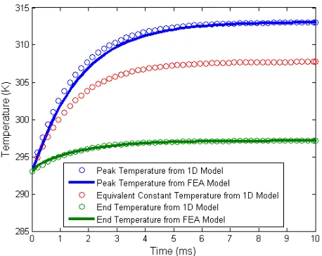
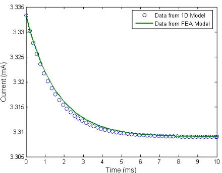
[image:9.595.179.408.276.458.2]For validation of this last result, eq. 20 was solved in isolation using a fourth order Runge-Kutta algorithm in Simulink. For clarity, the term related to the heat exchange through the insulator was omitted. This was then compared to the transient response of the isolated active sink calculated using FEA in Comsol shown in Fig. 4. In Fig. 6 the peak temperature and the end temperature of the active sink as calculated using FEA is compared to the temperatures as inferred from the results of the Simulink simulation and eqs. 13 and 18. The equivalent constant temperature as calculated from the Simulink model is also plotted for comparison. It is important to note that it took over twenty minutes to solve the full 3-D model of the active sink with FEA and less than ten seconds to solve the equivalent 1-D case in Simulink.
Fig. 6: The transient response of the end and peak temperature of the active sink when 1 V is passed it on its own. Note that the 1-D model corresponds well to the full 3-D model solved using
FEA.
Fig. 7: The transient response of the current when 1 V is passed through the active sink on its own. Note that the 1-D model corresponds well to the full 3-D model solved using FEA. To summarise, it has been shown that the heat exchange through the insulator and protective skin layer can be expressed as eq. 3. It has also been shown that the thermo-electric response of the sensor layer and the active sink can be given as eq. 8 and eq. 20 respectively. As the response of one layer is directly affected by the response of neighbouring layers, the governing equations are coupled and hence an analytical solution is unlikely. Fortunately, now the problem is in this reduced form, a numerical solution is possible.
4. Feedback System
The purpose of using an active sink as part of the device is to prevent heat loss from the temperature sensor to the substrate. This allows the heat flux through the polymer layer due to changes in external temperature to be directly measured by the temperature sensor. For this to work, the temperature of the active sink and the temperature sensor has to set to the same constant value. This can be seen if eq. 2 is applied to the temperature sensor. If the temperature is kept constant, the rate of accumulation of energy is zero. Similarly, if the active sink is at the same temperature as the sensor, there is no loss to the substrate. Therefore if the accumulation and loss of energy is zero, the rate of energy coming into the sensor must equal the rate of energy being generated. Put more simply, the change in heat flux through the polymer will equal the change in electrical power needed by the sensor to maintain its temperature, i.e. if the external temperature increases, the power through the sensor will decrease.
The feedback control to the active sink and temperature sensor consists of a simple proportional controller. By measuring each elements resistance at room temperature and temperature coefficient of resistance, eq. 7 can be used to determine the resistance of each element at the set temperature. In the case of this device, the initial specified temperature is to be set at 37.5 °C to be comparable to body temperature. During the experiment, the instantaneous resistance of each element is compared to the required resistance and normalised and the voltage is changed by the normalised resistance multiplied by a gain factor i.e.:
(21) 𝑉(𝑡) = 𝑉(𝑡 − 𝑑𝑡) + 𝑑𝑉 = 𝑉(𝑡 − 𝑑𝑡) + 𝐺𝑅𝑟𝑒𝑞−𝑅(𝑡)
where 𝑑𝑉 is the change in applied voltage, G is the gain, 𝑅𝑟𝑒𝑞 is the required resistance i.e. the resistance
calculated using eq. 7, 𝑅𝑜 is the resistance at room temperature and 𝑅(𝑡) is the instantaneous resistance.
In this way the resistance is kept constant and hence each elements temperature. The flux coming through the polymer layer is then monitored by measuring the electrical power through temperature sensor. The power through the sink will be essentially constant except at times of rapid external temperature change where there will a small change before it returns to its usual level. Clearly implementation of more sophisticated feedback systems is quite simple, but not necessary.
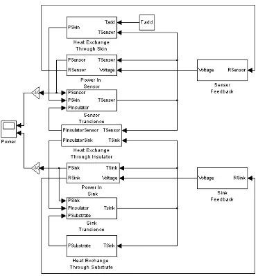
4.1 Solution of Model
As was mentioned previously, the system model for the entire device can be solved using Simulink, see Fig. 8 for the model. The algorithm is as follows:
1. Initially it is assumed that all layers are in thermal equilibrium and are at substrate temperature. There is initially no power going to the active sink and temperature.
2. In the first time step the resistance of the temperature sensor and active sink is measured and compared to the required resistance equivalent to the initial specified elevated temperature (37.5 °C) and the voltage is increased accordingly.
3. This results in a change in temperature of the sink and sensor. Given these temperatures as boundary conditions, the temperature profile throughout the insulation and polymer layer is found by solving eq. 3 using the Crank-Nicolson method as discussed in Appendix B. This is achieved using an embedded Matlab code in Simulink. The heat flux being transferred to/from the sink and sensor can be found by differentiating the temperature profile in the insulation/polymer layer respectively at the interface as per eq. 5. This then determines the heat flow into and out of the electrically heated layers.
4. The instantaneous temperature of the temperature sensor is then found by integrating eq. 8 using the fourth order Runge-Kutta solver with discreet time-stepping built into Simulink.
5. Similarly, the instantaneous temperature of the active sink is found by integrating eq. 20 in the same manner as the sensor.
6. The temperatures are then used to find the resistances of the active sink/temperature sensor using eq. 7.
7. Given the resistance and the applied voltage, the electrical power passing through the sensor is measured using eq. 6.
8. In the next time step, the resistances are compared again to the desired resistances and the voltages being applied to the active sink/temperature sensor is again changed accordingly. The sequence from step 3 to 8 is repeated for the necessary number of time steps.
Fig. 8: The Simulink model depicting how the different layers are linked together.
5. Results
For the purposes of simulation, it will be assumed that the temperature sensor will be made out of a gold layer 200 nm thick and with the same width and length as the active sink. The insulation layer and polymer layer will be assumed to have the same properties as PDMS for simplicity. The insulation layer will be 10 μm thick and the protective polymer layer will be 100 μm. The properties of the layers are:
Gold PDMS
Thermal conductivity ( 𝑊/(𝑚. 𝐾)) 318 0.15
Electrical Resistivity (Ω m) 2.23e-8 10e12
Temperature coefficient of resistance (1/𝐾) 3.768e-3 -
Specific heat (𝐽/(𝑘𝑔. 𝐾)) 129 1460
Density (𝑘𝑔/𝑚3) 19320 970
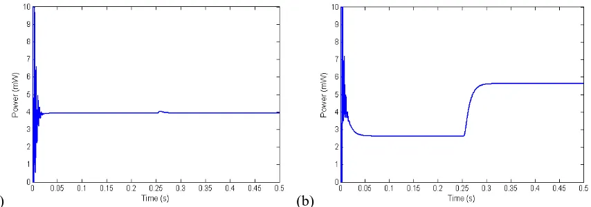
[image:12.595.97.506.640.724.2]It should be noted that gold was considered as it is compatible with a number of MEMS fabrication facilities. Other materials, perhaps with a higher temperature coefficient of resistance or electrical resistivity, could be used if convenient. The time, 𝑑𝑡, for each integration step is 1 μs. The gain for the active sink proportional controller was set to 1 and for the temperature sensor was set to 0.05. It was assumed that the controllers would measure the resistances of the pertinent layers and change their voltages accordingly every 0.1 ms. The initial sensor temperature was set to 310.5 K, as before, and the external temperature was set to room temperature (293 K) until 0.25 s when the device was instantaneously brought into contact with an object at 273 K. The response for the active sink and temperature sensor can be shown to be:
(a) (b)
Fig. 9: (a) The response of the active sink to a change in external temperature of -20K and (b) the reponse of the temperature sensor.
There are several features that are worth noting in the response of the active sink and temperature sensor. The first is the initial transience. As the sink and sensor are starting from room temperature and need to be heated to 310.5 K there is tendency for the contoller to overshoot before settling down to the correct temperature, especially if the sampling time of the controller is large. It is also important to note that while the tempertaure was changed instantly it took the temperature sensor about 0.1 s to reach steady state. This is important because the external temperature can only calculated analytically if the temperature gradient throughout the polymer layer is known. And while is can be predicted using solutions such as that given in Appendix A, in reality it is likely only to known exactly when the gradient is constant i.e. when the sensor is at steady state. It is interesting to note the small increase in power in the active sink before rurning to normal as it compensates for the sudden heat loss in the temperature sensor.
It should be not that such changes in power and even the small changes in the resistances of the gold layer are easily achieved using modern digital multimeters, such as the NI 4070 [30], which is capable of measuring 1 V at 1 µV resolution and 20 mA at 10 nA resolution, and therefore can measure resistances to c.a. 60 µΩ and powers to 23 nW at the appropriate level to seven digits at 5 S/s, which is more than sufficient. Cheaper options can be created using multimeter ICs, such as the MAX1367 [31], to provide sufficient resolution.
[image:13.595.88.515.220.370.2]Fig. 10: The heat flux passing from the sensor into the polymer layer. Note how it increases when the temperature gradient decreases.
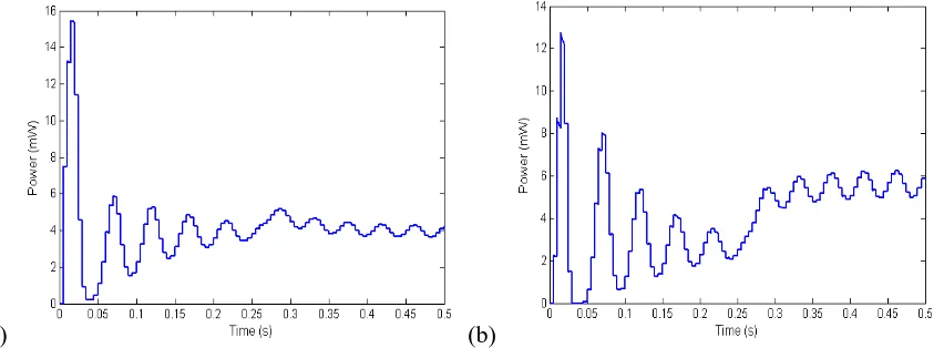
The effect of the control mechanism can be quite profound. If the sampling rate is too low or the gain is too high, abhorrent behaviour can occur masking the effects of changing the external temperature. For example in Fig. 11 the response of the active sink and temperature sensor are given again for the system described above but with the sampling time increased to 5 ms. Even with the gains for the active sink and temperature sensor controller reduced to 0.5 and 0.05 respectively, the behaviour is not ideal. This will dictate what technology is used for the controllers.
(a) (b)
Fig. 11: (a) The response of the active sink to a change in external temperature of -20K given a reduction in the sampling rate of the feedback controller to 5 ms and (b) the reponse of the
temperature sensor.
[image:14.595.81.507.383.540.2]Fig. 12: The responses of the temperature sensor due to changes in the external temperature. dText indicates the difference from room tempertaure (293 K). Note how the time to reach steady
state is the same in all cases.
The responses given in Fig. 12 show a trend which is more clearly seen in Fig. 13. Fig. 13 shows how the steady state response changes when the external temperature is changed from room temperature. It can be seen that the difference in the steady state power levels in the sensor as compared to the steady state power level at room temperature is a linear function of the change in external temperature. This is likely to be due to the assumption that the resistance of the sensor has a linear dependance on temperature as given in eq. 7.
[image:15.595.134.470.74.288.2]
Fig. 13: The relationship between change in external temperature from room temperature and the change in electrical power used by the temperature sensor. Note how the relationship is
6. Fabrication
As mentioned above, whilst there are several designs that are possible, they are all equivalent to each other provided that the sensor consists of two conductive elements (the diaphragm and substrate) separated by an electrically, but not thermally, insulting layer (the oxide layer in this example). The design configuration below provides an additional common ground between the detecting layer and the active sink. If the pressure sensor was as described above, i.e. fabricated on a bonded silicon-on-insulator (BSOI) wafer coated with a polymer layer for protection with the diaphragm being released through selective etching of the insulating oxide layer, as is quite common, then a simple process plan to fabricate the temperature and capacitive sensors together is possible. A possible plan is given below:
1. Start with BSOI wafer
2. DRIE to define active sink
3. Use lift off to deposit input electrode on active sink
4. Deposit SU8 for insulation layer
5. Using lift off deposit thermal sensor and ground electrode
6. HF release
7. Conclusions
and temperature sensor have individual proportional controllers allowing their temperatures to be maintained at a constant equal value, regardless of the external temperature. By keeping the active sink and temperature sensor at an equal temperature, it has been shown that heat loss from the temperature sensor to the substrate is prevented, so that the change in heat flux due to change in the external temperature can be directly and accurately measured.
Even though it is inherently a three dimensional structure, the thermo-electrodynamics has been simplified into a one dimensional Simulink model which allows for the response of the sensor to be known. The model incorporates the effect of the temperature profile in the insulation layers as well as the transient nature of heat generation. In this manner the heat exchange mechanisms between the layers have been fully modelled. The fabrication plan for these sensors has also been described.
Acknowledgments
This research was undertaken within the FP7-NMP NANOBIOTOUCH project [contract no. 228844]. The authors are grateful for the financial support provided by the EC.
References
[1] Bogue, R. (2007). MEMS sensors: past, present and future. Sensor Review, 27(1), 7-13.
[2] Eaton, W. P. and Smith, J. H., (1997), Micromachined Pressure Sensors: Review and Recent Developments, Smart Mater. Struct., Vol. 6, pp. 530-539
[3] Kumar, S. S., & Pant, B. D. (2014). Design principles and considerations for the ‘ideal’silicon piezoresistive pressure sensor: a focused review. Microsystem technologies, 20(7), 1213-1247. [4] Lee, Y. S., & Wise, K. D. (1982). A batch-fabricated silicon capacitive pressure transducer with
low temperature sensitivity. IEEE transactions on electron devices, 29(1), 42-48.
[5] Pramanik, C., Islam, T., & Saha, H. (2006). Temperature compensation of piezoresistive micro-machined porous silicon pressure sensor by ANN. Microelectronics Reliability, 46(2-4), 343-351.
[6] Maheshwari, V., & Saraf, R. (2008). Tactile devices to sense touch on a par with a human finger. Angewandte Chemie International Edition, 47(41), 7808-7826.
[7] Beebe, D. J., Hsieh, A. S., Denton, D. D., & Radwin, R. G. (1995). A silicon force sensor for robotics and medicine. Sensors and Actuators A: Physical, 50(1-2), 55-65.
[8] Almassri, A. M., Wan Hasan, W. Z., Ahmad, S. A., Ishak, A. J., Ghazali, A. M., Talib, D. N., & Wada, C. (2015). Pressure sensor: state of the art, design, and application for robotic hand. Journal of Sensors, 2015.
[9] Besse, N., Rosset, S., Zarate, J. J., & Shea, H. (2017). Flexible active skin: large reconfigurable arrays of individually addressed shape memory polymer actuators. Advanced Materials Technologies, 2(10).
[10] Cruz, M. P., Fiedler, E., Monjarás, O. C., & Stieglitz, T. (2015). Integration of temperature sensors in polyimide-based thin-film electrode arrays. Current Directions in Biomedical Engineering, 1(1), 529-533.
[11] Hong, H. B. (2017). U.S. Patent Application No. 15/208,095.
[13] Kim, J., Kim, J., Shin, Y., & Yoon, Y. (2001). A study on the fabrication of an RTD (resistance temperature detector) by using Pt thin film. Korean Journal of Chemical Engineering, 18(1), 61-66.
[14] Maiti, T. K. (2006). A novel lead-wire-resistance compensation technique using two-wire resistance temperature detector. IEEE Sensors Journal, 6(6), 1454-1458.
[15] Osborne, D. W., Flotow, H. E. and Schreiner, F., (1967), Calibration and Use of Germanium Resistance Thermometers for Precise Heat Capacity Measurements from 1 to 25°K High Purity Copper for Interlaboratory Heat Capacity Comparisons, Rev. Sci. Instr., Vol. 38
[16] Cheneler, D., Teng, J., Adams, M., Anthony, C. J., Carter, E. L., & Ward, M. (2011). Printed circuit board as a MEMS platform for focused ion beam technology. Microelectronic Engineering, 88(1), 121-126.
[17] Rochus, V., Wang, B., Tilmans, H. A. C., Chaudhuri, A. R., Helin, P., Severi, S., & Rottenberg, X. (2016). Fast analytical design of MEMS capacitive pressure sensors with sealed cavities. Mechatronics, 40, 244-250.
[18] Blasquez, G., Naciri, Y., Blondel, P., Moussa, N. B., & Pons, P. (1987). Static response of miniature capacitive pressure sensors with square or rectangular silicon diaphragm. Revue de physique appliquée, 22(7), 505-510.
[19] Lee, Y. S., & Wise, K. D. (1982). A batch-fabricated silicon capacitive pressure transducer with low temperature sensitivity. IEEE transactions on electron devices, 29(1), 42-48.
[20] Chen, Y. M., He, S. M., Huang, C. H., Huang, C. C., Shih, W. P., Chu, C. L., ... & Su, C. Y. (2016). Ultra-large suspended graphene as a highly elastic membrane for capacitive pressure sensors. Nanoscale, 8(6), 3555-3564.
[21] Cheng, M. Y., Huang, X. H., Ma, C. W., & Yang, Y. J. (2009). A flexible capacitive tactile sensing array with floating electrodes. Journal of Micromechanics and Microengineering, 19(11), 115001.
[22] Bottomley, J. T., (1882), James Prescott Joule, Nature, Vol. 26, pp. 617-620 [23] Verdet, E., (1872), Théorie Méchanique de la Chaleur, Vol. 2, pp. 197
[24] Davies, E. J., (1990), Conduction and Induction Heating, IEE Power Engineering Series, IET [25] Welty, J. R., Wicks, C. E., Wilson, R. E. and Rorrer, G., (2001), Fundamentals of Momentum,
Heat and Mass Transfer, 4th Ed., Wiley & Sons, pp. 159-168
[26] Carslaw, H. S. and Jaeger, J. C., (1959), Conduction of Heat in Solids, 2nd Ed., Clarendon Press
[27] Borse, G. J., (1997), Numerical Methods with MatLab: a Resource for Scientists and Engineers, PWS Publishing Co.
[28] Siakavellas, N. J. and Georgiou, D. P., (2005), 1D Heat Transfer Through a Flat Plate Submitted To Step Changes in Heat Transfer Coefficient, Int. J. Therm. Sci., Vol. 44, pp. 452-464
[29] Multiphysics, C. O. M. S. O. L. (2011). Version 4.2, COMSOL. Inc., http://www. comsol. com. [30] Specifications PXI-4070 (2017). Report 371304J-01, NI.com. Available at:
http://www.ni.com/pdf/manuals/371304j.pdf [Accessed 25 Jun. 2018].
[31] MAX1365/MAX1367. (2006). Maxim. Available at: https://datasheets. maximintegrated.com/en/ds/MAX1365-MAX1367.pdf [Accessed 25 Jun. 2018].
Appendix A
As was previously mentioned, eq. 3 does have an analytical solution. In the context of the numerical integration scheme discussed above, only the change in the temperature distribution, 𝑇(𝑥), during each fixed time step, 𝑑𝑡, is required as this gives the heat flux flowing in/out of the layers surface. In general the temperature distribution and the associated end temperatures, 𝑇1,2, of the insulation/polymer layer
are continuous functions of time. However, in the numerical scheme, it is assumed that the end temperatures are constant for the duration of the fixed time step. Therefore the boundary conditions to be used in the solution of eq. 3 are:
(A.1)
where 𝑡′ is the time during each time step i.e. 0 ≤ 𝑡′ ≤ 𝑑𝑡. The initial condition is the temperature distribution, 𝑔(𝑥), inherited from the solution of the previous time step. When 𝑡 = 0 it is assumed the whole structure is in thermal equilibrium with the environment and therefore the initial condition can be stated as:
(A.2) 𝑇(𝑥, 0) = 𝑇𝑅 𝑡 = 0
𝑇(𝑥, 0) = 𝑔(𝑥) 𝑡 > 0
where 𝑇𝑅 is the room temperature in 𝐾. As surface conditions are assumed to be independent of time
during each time step, the general problem can be simplified to that of two problems, one of steady temperature and one of variable temperature with prescribed initial temperature and zero surface temperature [26]. Put:
(A.3) 𝑇 = 𝑢 + 𝑤
where 𝑢 and 𝑤 satisfy the following equations:
(A.4) 𝑑 2𝑢
𝑑𝑥2= 0 (0 < 𝑥 < 𝐿) (A.5) 𝑢 = 𝑇𝑢 = 𝑇1, 𝑤ℎ𝑒𝑛 𝑥 = 0
2, 𝑤ℎ𝑒𝑛 𝑥 = 𝐿
and
(A.6) 𝜕𝑤
𝜕𝑡 = 𝛼 𝜕2𝑤
𝜕𝑡2 (0 < 𝑥 < 𝐿) (A.7) 𝑤 = 0, 𝑤ℎ𝑒𝑛 𝑥 = 0 𝑎𝑛𝑑 𝑥 = 𝐿
(A.8) 𝑤(𝑥, 0) = 𝑔(𝑥) − 𝑢
Straightaway the solution to eq. A.4 can be given as:
(A.9) 𝑢 = 𝑇1+ (𝑇2− 𝑇1)𝑥/𝐿
If the initial temperature distribution, 𝑔(𝑥), can be expanded in the sine series:
(A.10) 𝑔(𝑥) ≅ ∑ 𝑎𝑛𝑠𝑖𝑛 𝑛𝜋𝑥
𝐿 ∞
𝑛=1
where 𝑎𝑛 = 2
𝐿∫ 𝑔(𝑥
′) 𝐿
0 𝑠𝑖𝑛
then:
(A.11) 𝑤(𝑥, 0) = ∑ 𝑏𝑛𝑠𝑖𝑛 𝑛𝜋𝑥
𝐿 ∞
𝑛=1
where 𝑏𝑛 = 2
𝐿∫ [𝑔(𝑥 ′) − 𝑇
1+ (𝑇2− 𝑇1) 𝑥′ 𝐿] 𝐿 0 𝑠𝑖𝑛 𝑛𝜋𝑥′ 𝐿 𝑑𝑥′
It is clear that the solution to eq. A.6 must be:
(A.12) 𝑤(𝑥, 𝑡′) = ∑ 𝑏𝑛𝑠𝑖𝑛 𝑛𝜋𝑥
𝐿 ∞
𝑛=1 𝑒−𝛼𝑛
2𝜋2𝑡′/𝐿2
And therefore:
(A.13) 𝑇(𝑥, 𝑡′) = 𝑇
1+ (𝑇2− 𝑇1) 𝑥 𝐿+
2 𝜋 ∑
𝑇2𝑐𝑜𝑠(𝑛𝜋)−𝑇1
2𝑛+1 𝑠𝑖𝑛 𝑛𝜋𝑥
𝐿 ∞
𝑛=1 𝑒−𝛼𝑛
2𝜋2𝑡′/𝐿2
+ 2
𝐿∑ 𝑠𝑖𝑛 𝑛𝜋𝑥
𝐿 ∞
𝑛=1 𝑒−𝛼𝑛
2𝜋2𝑡′/𝐿2
∫ 𝑔(𝑥0𝐿 ′)𝑠𝑖𝑛𝑛𝜋𝑥′
𝐿 𝑑𝑥′
From eq. A.13 the temperature gradient at the surfaces of the layer can be found and hence the heat flux exchange into the layer in accord with eq. 5. When 𝑔(𝑥) is a simple, known function, an exact answer for eq. A.13 can be found. However, in general, 𝑔(𝑥) will be the solution of eq. A.13 for the previous time step and will only be known numerically. This means that in general eq. A.13 will need to be solved using numerical integration methods. The problem is that eq. A.13 tends to converge slowly and so the integral becomes highly oscillatory. While there are numerical integration methods that can be used effectively, such as that given in [32], an accurate numerical solution to eq. A.13 is prohibitively computationally expensive and so the method detailed in Appendix B is used instead.
Appendix B
Eq. 3 is a parabolic partial differential equation frequently encountered in heat transfer problems. It is well known that boundary and initial conditions of the form given in eq. B.1 are sufficient to ensure that the solution is unique [27].
(B.1)
𝑇(0, 𝑡) = 𝑓0(𝑡)
𝑇(𝐿, 𝑡) = 𝑓𝐿(𝑡)
𝑇(𝑥, 0) = 𝑔(𝑥)
In this case a solution is required for the region 0 ≤ 𝑥 ≤ 𝐿, 0 ≤ 𝑡 ≤ 𝑑𝑡, where 𝑑𝑡 is the time step in the systems numerical integration scheme. To solve this problem, a finite difference approach is used. Here a rectangular grid is superimposed on this region, with equal increments, ∆𝑥, in the space coordinate, and ∆𝑡 in the time coordinate. The grid points are then:
(B.2) 𝑥𝑡𝑖 = 𝑖∆𝑥 𝑖 = 0, … , 𝑁𝑥 ∆𝑥 = 𝐿/𝑁𝑥
𝑗 = 𝑗∆𝑡 𝑗 = 0, … , 𝑁𝑡 ∆𝑡 = 𝑑𝑡/𝑁𝑡
The Crank-Nicolson method can be used to solve this problem and has the advantage of being unconditionally stable and being second-order accurate in both ∆𝑥 and ∆𝑡 [27]. The finite difference expressions can be shown to be:
(B.3) 1
2(
𝑇𝑖+1,𝑗+1−2𝑇𝑖,𝑗+1+𝑇𝑖−1,𝑗+1
(∆𝑥)2 +
𝑇𝑖+1,𝑗−2𝑇𝑖,𝑗+𝑇𝑖−1,𝑗
(∆𝑥)2 ) = 𝛼
𝑇𝑖,𝑗+1−𝑇𝑖,𝑗
By defining:
(B.4) 𝛾 = ∆𝑡
𝛼(∆𝑥)2
eq. B.3 can be rearranged by collecting all the 𝑗 + 1 terms on one side to give:
(B.5) 𝛾
2𝑇𝑖+1,𝑗+1− (1 + 𝛾)𝑇𝑖,𝑗+1+ 𝛾
2𝑇𝑖−1,𝑗+1 = − 𝛾
2𝑇𝑖+1,𝑗+ (𝛾 − 1)𝑇𝑖,𝑗− 𝛾 2𝑇𝑖−1,𝑗
These equations can be collected together for a specific value of 𝑗 into a single matrix equation:
(B.6) 𝑨(𝛾)𝑇⃗ 𝑗+1= 𝑨(𝛾)𝑇⃗ 𝑗+1+ 𝑏⃗
where:
(B.7) 𝑨(𝛾) =
(B.8) 𝒃⃗⃗ = | |
1
2[𝑓0(𝑡0) + 𝑓0(𝑡1)]
0 ⋮ 0
1
2[𝑓𝐿(𝑡0) + 𝐿(𝑡1)]
| |
As the complete thermo-electric problem is being solved using a 4th order Runge-Kutta algorithm with
a small but fixed time step 𝑑𝑡, 𝑁𝑡 can be quite small and still produce accurate results. In this case 𝑁𝑡 =
10, and 𝑁𝑥 = 25. Even though the subsequent matrices are quite small and could be solved using matrix
division quite easily, due to the size of the complete problem and the resulting demands on computer memory eq. B.6 is solved using sparse matrix methods to reduce computation times [27].
1 + 𝛾 −𝛾
2 0 ⋯ 0
−𝛾
2 1 + 𝛾 −
𝛾
2 ⋯ 0
0 −𝛾
2 1 + 𝛾 ⋯ 0
⋮ ⋮ ⋮ ⋱ ⋮