ISSN Online: 2327-5227 ISSN Print: 2327-5219
DOI: 10.4236/jcc.2018.612005 Dec. 26, 2018 56 Journal of Computer and Communications
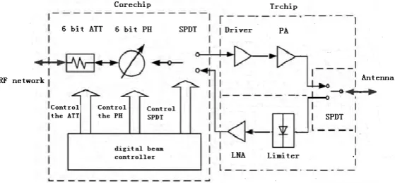
Tile Type Multi-Channel Transceiver Module
Applied for Phased Array Antenna
Fuzhou Tai, Jian Zhang
Southwest China Institute of Electronic Technology, Chengdu, China
Abstract
In order to reduce the volume and weight of phase array antenna in RF fre-quency, an integrated technology of multi-channel transceiver circuit and power division network in microwave is proposed for the tile type TR mod-ule. The component is integrated in a same dielectric substrate, the mounting interface of chips and power division network are on the same layer. Finally, a 8 × 8 array has been manufactured and tested to validate its function. The results show the integrated technology has good performance. It is very good to satisfy the miniaturization and lightweight of the T/R module in the active phased array antenna.
Keywords
Phased Array Antenna, TR Module, Power Division Network, High Density Integration
1. Introduction
Active phased array transceiver module is the key component of phase array an-tenna. The overall volume and weight of phase control antenna array depends on the individual T/R modules [1]. Therefore, from the beginning of 1980s, many countries engaged in research on how to reduce the volume and weight of a single T /R module with a large capital investment and scientific research strength [2]. Current research focuses on tile type structure of T/R module. Be-cause the volume of T/R module of tile type structure is only 1 /4 the size of the traditional brick structure [3]. So it has incomparable advantages of reduced vo-lume and weight, and it is easy to implement large-scale array [4].
This tile type T/R module uses PCB multilayer wiring technology. It is a high density integrated technology with 3 dimensional vertical transmissions. It can How to cite this paper: Tai, F.Z. and
Zhang, J. (2018) Tile Type Multi-Channel Transceiver Module Applied for Phased Array Antenna. Journal of Computer and Communications, 6, 56-63.
https://doi.org/10.4236/jcc.2018.612005
DOI: 10.4236/jcc.2018.612005 57 Journal of Computer and Communications high frequency PCB (RO 4360G2) is about 25 ppm/˚C; thermal expansion coef-ficient of Aluminium alloy or Copper alloy is about 20 ppm/˚C; therefore the substrate can be directly mounted on the Metal, without other transition. The dielectric constant is low: the dielectric constant is 5.9; it has excellent chemical stability and corrosion resistance, good weldability, and high strength, thus mak-ing it an ideal substrate material for high density packagmak-ing [7].
3. Design Analysis
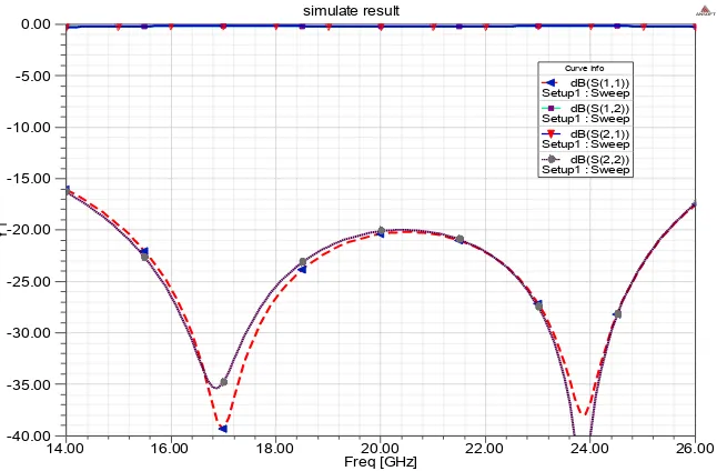
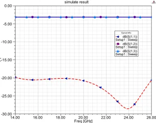
[image:2.595.235.515.578.708.2]The key points of the design are how to realize all the functions of the traditional T/R module with small volume. As a kind of new structure, the three-dimensional tile type T/R module with fuzz button used in the microwave frequency can achieve good DC and microwave links, and does not need welding. In the tradi-tional module, the microwave signal is transmitted into X-Y in 2D. In tile type T/R module microwave signal transferred not only in X-Y plane, but also in the Z axis direction. The use of PCB multi-layer wiring technology, through a rea-sonable layout, can realize good microwave performance. With metal isolation Cylinder, high frequency PCB multi-layer substrate can realize digital and ana-log signal isolation, and realize electromagnetic shielding to solve the problem of signal crosstalk. Three dimensional microwave signal simulation model of high frequency PCB substrate is shown in Figure 2 and Figure 3. The simulation re-sults are obtained as shown in Figure 4 and Figure 5.
DOI: 10.4236/jcc.2018.612005 58 Journal of Computer and Communications
[image:3.595.254.496.287.461.2]Figure 2. Simulation model of the microstrip coaxial transition.
Figure 3. Simulation model of the internal divider.
Figure 4. Simulation results of the above structure.
14.00 16.00 18.00 20.00 22.00 24.00 26.00
Freq [GHz] -40.00
-35.00 -30.00 -25.00 -20.00 -15.00 -10.00 -5.00 0.00
Y1
simulate result ANSOFT
Curve Info
[image:3.595.215.538.495.707.2]DOI: 10.4236/jcc.2018.612005 59 Journal of Computer and Communications
Figure 5. Simulation results of the internal divider.
From the simulation results we can see, in the K band, the transmission inser-tion loss of the vertical transiinser-tion of the high frequency PCB substrate is less than 0.5 dB, and the return loss is more than 15 dB.
The multi-channel transceiver circuit and power division network is very compact, 5 layers high frequency PCB substrate is used, 1.7 mm in thickness. The top 2 layers arrangement for microwave signal; the lower 3 layers arrange-ment for the various data control line and the power line. Bottom layer is ar-ranging for GND. According to the space arrangement, the form layout is shown in Figures 6-8. Among them, 1 for the multi-channel transceiver circuit module, 2 for power division network, 3 for dielectric substrate, 4 for low fre-quency control pad, 5 for power supply pad, 6 for RF port connected with an-tenna, 7 for transceiver common public port, 8 for low frequency control and power supply interface, 9 for metal isolation Cylinder, and 10 for solid grounded cylinder which conduct the thermal of the chip to the bottom of the printed board.
As shown in Figure 6, device mounting interface and power division network are in the same layer. In order to reduce the influence between circuit routing, all around use the metal isolation column to realize electromagnetic shielding. The low frequency control and the power supply of the chip are connected with pads near the chip. Below the pad there are metallized holes connected with the printed circuit board, as shown in Figure 7. At the same time, the solid grounded column designed under the chip mounting interface not only provide ground for the chip but also conduct the thermal of the chip to the bottom of the printed board, as shown in Figure 8.
14.00 16.00 18.00 20.00 22.00 24.00 26.00
Freq [GHz] -30.00
DOI: 10.4236/jcc.2018.612005 60 Journal of Computer and Communications
[image:5.595.259.487.292.464.2]Figure 6. Upper surface of integrated multilayer printed board.
Figure 7. Lower surface of integrated multilayer printed board.
[image:5.595.262.491.496.693.2]DOI: 10.4236/jcc.2018.612005 61 Journal of Computer and Communications
[image:6.595.242.506.437.703.2]Figure 9. The high frequency PCB multilayer substrate.
DOI: 10.4236/jcc.2018.612005 62 Journal of Computer and Communications
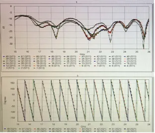
Figure 11. The Passive test results of each channel: S21 (dB) and S22 (dB).
Figure 12. The Passive test results of each channel: S11 (dB) and S21 (phase).
5. Conclusion
[image:7.595.218.531.377.645.2]DOI: 10.4236/jcc.2018.612005 63 Journal of Computer and Communications per.
References
[1] Heyen, J., von Kerssenbrock, T., Chernyakov, A., Heide, P. and Jacob, A.F. (2003) Novel LTCC/BGA Modules for Highly Integrated Millimeter-Wave Transceivers.
MTT-S, 51, 2589-2596. https://doi.org/10.1109/TMTT.2003.819210
[2] Meinel Holger, H. (1995) Commercial Applications of Millimeterwaves Present Status and Future Trends. IEEE Transactions on Microwave Theory and Tech-niques, 43, 1639-1653. https://doi.org/10.1109/22.392935
[3] Lai, I.C.H. and Fujishima, M. (2008) Design and Modeling of Millimeter-Wave CMOS Circuits for Wireless Transceivers. Springer, Japan.
[4] Gauthier, G., Bertinet, J.P. and Schroth, J. (2006) Low-Cost Ka-Band Transmitter for VSAT Applications. IEEE MTT-S International, Microwave Symposium Digest, 1398-1401. https://doi.org/10.1109/MWSYM.2006.249530
[5] Jin, L., Loyez, C., Rolland, N., et al. (2010) An UWB Millimeter-Wave Transceiver Architecture for Wireless Sensor Networks Applications. 40th European Microwave Conference, 377-380.
[6] Sai, W.W. and Lei, Z. (2008) Ultra-Wideband Power Divider with Good In-Band Splitting and isolation Performances. IEEE Microwave and Wireless Components Letters, 18, 518-520. https://doi.org/10.1109/LMWC.2008.2001009