Faculty of Electrical Engineering,
Mathematics & Computer Science
Impedimetric analysis of the
activity of single fluid cracking
catalyst particles
Jordi M. Hendrix M.Sc. Thesis 24 August 2018
Supervisors:
Fluid catalyst cracking (FCC) particles are crucial for the transformation of crude oil into usable products. The particle acts as catalyst to convert large hydrocarbon chains into, for instance, gasoline. During the cracking process, FCC particles become deac-tivated due to the accumulation of material. This causes a reduced efficiency of the cracking process. In the current cracking process, it is not possible to selectively re-move the deactivated particles. The possibility to detect FCC particle activity, by using the electrical impedance, was investigated in this thesis. Literature indicates a relation between the activity of FCC particles and the amount of metal that has been accu-mulated on the particle. Several models were made to relate this change in metal ac-cumulation to a measurable impedance of a microfluidic sensor. These models show that it is most favourable to measure the high frequency capacitance of the particles, while using anisole as medium. The expected change in capacitance of this system was modelled to be between 7 and 12aF. To measure this change in capacitance, a lock-in architecture was designed with a noise level of 6.3aF. The system was tested, while using anisole as medium, by measuring both air bubbles and polystyrene parti-cles. This resulted in expected system behaviour. During the final experiments, two categories of particles where measured: fresh and deactivated FCC particles. During these measurements, around 40 particles of each group where measured and video analysis was used to estimate the size of the particles. The experimental results were fitted into a cube function with respect to the particle radius. The experiments showed that impedance variations of FCC particles of the same category are more signifi-cant than impedance changes due to metal accumulation. Nevertheless, a correlation exists between the activity of a particle and the average impedance. For a particle with a radius of 40 micron, the experimental results showed an average difference in impedance between fresh and deactivated particles of 20.5F, which closely resembles the model results. Although more particles should be measured to verify this differ-ence, the average impedance of Fluid cracking catalyst (FCC) could potentially be used to identify groups of reduced activity.
Summary iii
List of acronyms vii
1 Introduction 1
2 Theory & modelling 3
2.1 Basic measurement principle . . . 3
2.1.1 Impedance elements . . . 3
2.1.2 Impedance detection in literature . . . 5
2.1.3 Unwanted effects . . . 9
2.2 Particle information . . . 10
2.3 Electrical analysis of electrode-particle system . . . 12
2.3.1 Model building . . . 13
2.3.2 Results and discussion . . . 22
2.4 Microfluidics . . . 28
3 Design 31 3.1 Microfluidic chip design . . . 31
3.1.1 Particle position dependence . . . 32
3.1.2 Differential measuring . . . 32
3.1.3 Design considerations . . . 33
3.2 Measurement set-up design . . . 35
3.2.1 Function generation . . . 35
3.2.2 Charge amplifier . . . 36
3.2.3 Lock-in amplifier . . . 37
3.2.4 Shielding compartment . . . 38
3.2.5 Remaining set-up elements . . . 38
4 Materials & methods 39 4.1 Materials . . . 39
4.1.1 Fluids . . . 39
VI CONTENTS
4.1.3 Equipment . . . 39
4.1.4 Software . . . 40
4.2 Methods . . . 40
4.2.1 Chip fabrication . . . 40
4.2.2 Plan of action . . . 41
5 Results and discussion 45 6 Conclusions 57 7 Recommendations 59 8 Acknowledgements 61 References 63 Appendices A Simulation results Tao Sun model: particle between electrodes 71 A.1 Optimization of electrode length and width . . . 71
A.2 Optimization of electrode spacing . . . 73
A.3 Optimization of fluid dielectrics . . . 75
A.4 Particle size variation . . . 77
B Process flow 79
C Mask layout 89
FCC Fluid cracking catalyst
Fe Iron
Ni Nickel
V Vanadium
LML low metal loading
MML medium metal loading
HML high metal loading
DC direct current
AC alternating current
SiO2 Silicon dioxide
Introduction
FCC particles are used in 40-45% of the gasoline production in the world [1]. The particles are used as a catalyst to cut long chain hydrocarbons into smaller molecules which can then be used in the production of fuels and chemicals. A schematic de-scription of the cracking process is shown in Fig. 1.1. The cracking of oil is an en-dothermic reaction which takes place in a reactor by using the catalytic properties of FCC particles. When being used, the FCC particles become deactivated due to the accumulation of several metals (Iron (Fe), Nickel (Ni) and Vanadium (V)) and/or coke, mainly on the particle surface [2]–[5]. The accumulated coke is removed by thermal regeneration, after which the FCC particles return into the cracking process. However, the accumulated metals can not be removed, causing deactivation of the particles over time. This deactivation will decrease the efficiency of the gasoline production process and requires the FCC particles to be continuously replaced for fresh ones. An estimated 2.3 million kilogram of particles are used each day [6].
Fig. 1.1:Process flow of oil cracking using FCC particles [6].
2 CHAPTER1. INTRODUCTION
In the current cracking process, it is not possible to selectively remove the deac-tivated catalyst particles. Instead a small percentage of the total FCC particles is removed and replaced with fresh ones at specific intervals. Therefore, some particles that are removed will still be active, while other particles that are deactivated will re-main in the process. This will reduce the efficiency of the FCC cracking process and creates an unnecessary waste of usable FCC particles. A method to continuously de-tect the activity of FCC particles would give rise to the possibility to selectively remove the deactivated FCC particles, reducing these negative effects.
Several methods to detect the activity of FCC particles has been recorded in liter-ature. Meier et al., uses the skeletal density to measure the activity [1]. The density of the particles slowly increase during the cracking process due to the accumulation of material. As the accumulated material causes deactivation of the particle, the den-sity gives an indication for the activity of the particle. The increase in denden-sity can be detected by the sink-float density separation method. The limitation of this method is that it cannot be used continuously to separate the FCC particles. Furthermore, this method detects accumulation of any particles and not specifically the accumulation of the materials which causes particle deactivation.
Another method to separate the FCC particles with a difference in activity is based on the magnetic properties, as done by Solsona et al. [7]. The accumulation of iron on the particle, which is partly responsible for the deactivation, makes the particle magnetic. The deactivated particles can thus be separated with the use of magnetic forces. A limitation of this technique is that only the iron accumulation is detected, while this is not the only element responsible for deactivation of FCC particles.
In this thesis, it is determined whether it is possible to detect the activity of FCC particles by using the electrical properties of the particle. An advantage of this tech-nique is that the detection is not limited to one specific metal, like the techtech-nique of Solsona [7]. The technique is sensitive to any accumulation in material and not just the activity-reducing elements. However, unlike in the technique of Meier, the sensi-tivity is dependent on the element. This allows a design were the acsensi-tivity-reducing metals are detected with highest sensitivity [1]. In this research, the following question is answered: ”Can the metal accumulation of fluid catalyst cracking particles during crude oil processes be detected by measuring the particle impedance?”
Theory & modelling
In this chapter, the theory and models that are used to describe the designed system are explained. The chapter starts with some basic information about the measurement principle which is used. This includes a description of the detection methods which are used in literature. Hereafter, the relevant information about the FCC particles will be given. Next, the electrical models used to characterize the system will be explained in detail. The results of these models are used in the design of both the microfluidic chip and the measurement circuit which are used in experiments. Finally some information is given about the microfluidics as used in the system.
2.1 Basic measurement principle
The goal of this research is to detect the activity of FCC particles by using the electrical impedance. The impedance of a system is a measure for the ratio between the applied voltage and the current flowing through this conductor. To measure the impedance of FCC particles, two electrodes are used. When the particle is present between the electrodes, the measured impedance will partly be determined by the electrical properties of the particle. The measurement will be performed in a microfluidic chip, where the FCC particles will one by one pass the electrodes by flowing along with the fluid. A simplified schematic of the measurement design is shown in Fig. 2.1.
2.1.1 Impedance elements
The impedance of the system can be subdivided into three basic circuit elements: the resistance, the inductance and the capacitance. When using constant non-changing voltages (direct current (DC)), the impedance of a conductor is completely determined by the resistance. However, when using alternating current (AC) voltages, also the capacitance and inductance are included in the impedance.
4 CHAPTER 2. THEORY &MODELLING
Fig. 2.1: Simplified schematic of the chip design that is used to measure the impedance of FCC particles, modified from [8]
Resistance
The resistance describes how well an element resists the flow of current through this material. For the system of Fig. 2.1, the resistance is determined by both the fluid and FCC particle, which are located in-between the electrodes. During experiments, the choice of liquid is thus important. The fluid resistivity, which is the resistance per unit length, is one of the properties, which determines the liquid choice. The resistance of an element can be determined from the resistivity by:
R = ρd
A, (2.1)
where R represents the resistance [Ω], ρ the resistivity [Ωm], d the distance be-tween the electrodes [m] andAthe area of the electrodes [m2].
Inductance
An inductor is an electrical element which is able to store energy in a magnetic field. As a result of a flowing current, a magnetic field is generated. Energy is required to change the strength of the stored magnetic field. An inductive element thus resists the change in magnetic field and therefore a change in current through a material. Inductance is mainly visible in very long wound wires, such as coils. As these wires are not present in the system of Fig. 2.1, the inductance becomes negligible.
Capacitance
dielectric material. Whenever a voltage difference is applied to the electrodes, charge accumulates on sides of the electrodes. This charge is equal in magnitude on both sides, but is positive on one electrode and negative on the other. For the device of Fig. 2.1, the capacitance dominates the system impedance, whenever the resistance of the fluid and particle is sufficiently large. The capacitance itself depends on the dimensions of the device, in combination with the dielectric properties of both the fluid and the particles:
C= 0rA
d , (2.2)
whereC represents the capacitance [F],0 the vacuum permittivity [F/m],r the di-electric constant [],Athe area of the electrode plates [m2] anddthe distance between
the electrodes [m]. The dielectric constant of the fluid is another important property on which the fluid choice is based upon.
2.1.2 Impedance detection in literature
There are several methods which can be used to detect the impedance of a system. As will be shown, small differences in particle electrical properties have to be detected, very sensitive measurements principles are required. Some common detection tech-niques used in literature are shortly described here.
Resonating circuit
Resonating circuits are based on the series or parallel combination of a capacitor and a inductor as shown in Fig. 2.2 [9]. The impedance of a capacitor and a inductor are as follows:
ZC =− j
ωC (2.3)
ZI =jωL, (2.4)
where Z indicates the impedance, C the capacitance [F] and L the inductance [H], ω the angular frequency [rad/s] and j the imaginary unit. At the specific angular frequency as shown in Eq. 2.5, both impedances are exactly equal in magnitude but one is positive, while the other is negative. At this frequency, the impedance of a resonance circuit shows a large peak which is relatively easy to detect. In resonating sensing circuits, the capacitor is the sensor with a variable capacitance. The change in capacitance will cause a changing resonance frequency which is detected.
ω = √1
6 CHAPTER 2. THEORY &MODELLING
Fig. 2.2: Example of resonance circuits, showing series and parallel resonance [10].
An example of a resonance circuit used in detecting the capacitance of a sensor is shown in Ferrier et al. [11]. By using a cavity resonator, a resolution of 2aF is reached, while detecting yeast cells and polystyrene beads in a microfluidic chip. Another ex-ample is the research of Tapson et al., where a resolution of 11aF is reached while detecting the movement of piezoelectric actuators [12].
Lock-in architecture
Another method to accurately measure the impedance of a system is to use a lock-in amplifier. This device is able to detect very small AC signals, even when the noise that is present, is several orders of magnitude higher than this signal. [13] This is possible since a lock-in amplifier is able to measure at a very narrow frequency bandwidth, which can be determined by the user. The basic building blocks of a lock-in amplifier are shown in Fig. 2.3.
Fig. 2.3: Block diagram showing the basic elements of a lock-in amplifier [14].
Fig. 2.4: Principle of noise reduction of a lock-in amplifier, modified from [19]
principle of a lock-in amplifier is based on multiplication of two sinusoidal functions. Whenever two sinusoidal signals are multiplied, the result is as shown in Eq. 2.6.
Asin(2πω1t)·Bsin(2πω2t) =
1 2AB
cos(2πt(ω1−ω2))−cos(2πt(ω1+ω2))
(2.6)
Where ω1 and ω2 are the frequencies of the two signals in [rad/s]. Whenever the
reference frequency is chosen such that frequencies ω1 and ω2 are exactly equal, the
result of the multiplication is a combination of a DC signal and a signal with twice the frequency. After using a simple low-pass filter, only the DC element will remain. The noise which is present, is a combination of 1/f noise and white noise and will therefore mostly be present at low-frequencies [15]–[18]. This noise is also multiplied with the reference signal, which will not result in a DC signal for all frequencies which are not exactly equal to the reference signal. After low-pass filtering most noise will therefore be removed. Only the noise, which has a frequency very close to the reference signal will thus remain. This principle is shown in Fig. 2.4
Wei et al. uses a lock-in architecture to measure the capacitance of a MEMS sus-pended blade in-between a set of electrodes [19]. This system is capable of detecting changes in capacitance for a capacitance of 1.2fF, with a resolution of 1aF for using a bandwidth of 100Hz.
Bride circuits
8 CHAPTER 2. THEORY &MODELLING
bridge configurations possible, depending on the measurement requirements. The simplest bridge circuit is the Wheatstone bridge as shown in Fig. 2.5.
Fig. 2.5:Circuit diagram of a Wheatstone bridge [20].
In this circuit Rx can be the sensor, for which the resistance is dependent on the measurement. Furthermore,Rais an internal variable resistor of the bridge circuit. In this bridge circuit, the null detector checks whether the potential at both branches of the bridge are exactly equal. In that case the bridge is so-called balanced and the value of the unknown resistorRx can be expressed as a function of the other, known, resistors Ra,R1 andR2. When the resistance ofRx changes, the bridge becomes unbalanced, which is detected by the null detector. The bridge circuit will then change the resistance value ofRa, until the bridge is balanced once again. Whenever balanced, the unknown resistor value can be calculated once again.
Besides the Wheatstone bridge as shown in Fig. 2.5, which is used for resistor calculations, also other bridge configurations are available. For instance, the Schering bridge can be used to measure capacitance values.
The disadvantage of using bridge circuits, is that the system is optimized for null de-tection, which requires constant calibration of some internal resistors and capacitors, which limits the measurement speed. For the AH2700A Ultra-precision 50Hz-20kHz Capacitance bridge, the resolution is about 0.5aF [21]. However, about 0.4 seconds is required for full precision measurements. This relatively low speed can thus be a problem for continuous flow measurements.
Opacity
differentiation. The opacity is defined as the ratio between high frequency and low fre-quency impedance and as found in Gawad et al. this opacity can largely compensate for size differences [22]. The low frequency impedance, which is the resistance will give the information about the particle size, which can be used in the high frequency measurement to allow for size compensation.
2.1.3 Unwanted effects
There are two important effects, which will limit the accuracy of any capacitive mea-surement system: parasitic capacitance and noise. The effect of these unwanted effects should be limited.
Parasitic capacitance
The parasitic capacitance of the sensor is the unwanted additional capacitance due to electric field lines outside the sensing area. The equation for a capacitor, as shown in Eq. 2.2, is a simplification of the real capacitance and does not include these fringing effects. When the separation of the electrodes is in the same range as the electrode dimensions, the total capacitance can be around 10 times the theoretical capacitance [23]. Parasitic effects can be reduced by shielding the electrodes [24].
Noise
Noise reduction is crucial when measuring small signals. To be able to measure a relevant signal, this signal should not be completely overshadowed by the present noise.
Noise in resistors and capacitors consists of Johnson-Nyquist noise due thermal fluctuations and 1/f noise which has a variety of causes [15]–[18]. As the 1/f noise decreases with frequency, this noise can be avoided by performing measurements at a high frequency. Johnson-Nyquist noise can however not be completely avoided and will thus always limit the accuracy of a measurement. For a resistor, the Johnson-Nyquist noise is:
in= p
4kbT∆f R, (2.7)
wherein is the root mean square of the current [A], kb is the Boltzmann constant [J/K], T is the temperature [K],R is the resistance [Ω] and ∆f is the frequency band-width that is used [Hz] [25]. The noise source will act as current noise source which is in parallel with the wanted resistor. When applying a voltage Vin to this noisy resistor, the noise current will cause a uncertainty in the measured resistance of:
Rn = Vin ir+in
10 CHAPTER 2. THEORY &MODELLING
where Rn is the uncertainty in measured resistance [Ω] and ir is the current of noiseless resistor with the fixed resistance ofR to which a potentialVin is applied [A]. The Johnson-Nyquist noise on a capacitor can be described by:
Qn = p
kbT Cmeas∆f , (2.9)
whereQnis the fluctuations in charge due to Johnson-Nyquist noise [C] andCmeas is the measured capacitance [F] [26]. From the fluctuations in charge on the capacitor, the change in capacitance can be determined by:
Cn = Qn Vcap
, (2.10)
where Cn is the capacitance fluctuation due to noise and Vcap is the voltage ap-plied to the capacitor. The capacitance noise can be reduced by minimizing the total capacitance, which can be done by avoiding parasitic capacitance. Furthermore, the frequency bandwidth can be reduced and the applied voltage can be increased.
2.2 Particle information
Little is known about the electrical properties of FCC particles, which complicates the modelling process. In order to model the electrical properties of these particles, the information about the composition is used, which is provided by the particle supplier. This information is listed in Tab. 2.1.
Tab. 2.1: Mass percentage of the content of FCC particles as provided by the supplier .
Component SiO2 Al2O3 MgO TiO2 Fe2O3 P2O5 CeO2
Mass percentage (%) 56.855 40.354 1.96 1.627 0.93 0.343 0.285
Na V2O5 CaO NiO K ZnO Cu
0.207 0.141 0.132 0.126 0.064 0.06 0.005
In the given information, the total mass percentage obtained by adding all the indi-vidual values is larger than 100%. It is unknown why this is the case, but to compen-sate all the percentages are scaled down.
Tab. 2.2: Change in the mass percentages of the molecules responsible for FCC par-ticle deactivation [1].
Mass percentage (%) Molecule Fresh LML MML HML Fe2O3 0.34 0.79 0.93 0.96
NiO 0.00 0.33 0.49 0.59 V2O5 0.00 0.53 0.66 0.74
Fig. 2.6: The concentration of iron close to the particle surface for different stages of metal accumulation (adapted from [1]).
Meirer et al. shows that the accumulation of some of the activity-reducing metals, is mainly occurring in the outer layer of the FCC particle [1]. Furthermore, this re-search shows that the reduction in the activity of FCC particles is mostly caused by the accumulation of metals on this outer layer. For iron, this accumulation is shown in Fig. 2.6. A similar concentration distribution is visible for nickel [1]. For vanadium the information about the concentration distribution is not available and it is assumed that this element is distributed equally over the particle.
12 CHAPTER 2. THEORY &MODELLING
Tab. 2.3: Important properties of the FCC content.
Component Dielectric constant Resistivity (Ω·m) Density (kg/m3)
SiO2 3.9 [27] 1012[28] 2650 [27]
Al2O3 9.9 [29] 1012[29] 3960 [29]
MgO 9.96 [30] 1012[31] 3580 [31]
TiO2 63.7 [32] 1010[33] 4230 [33]
Fe2O3 20.6 [34] 2.5·103 [35] 5260 [36]
CeO2 23 [37] 3.1·105 [38] 7110 [39]
V2O5 25 [40] 102 [40] 3357 [41]
CaO 12.01 [42] 5·106 [43] 3340 [44]
NiO 11.9 [45] 1.05·105 [45] 6800 [45]
ZnO 8.5 [46] 7.5·105 [47] 5660 [46]
Tab. 2.4: The amount of volume occupied by the medium due to the porosity of the FCC particle [1].
Fresh LML MML HML
Micropore volume (cm3/g) 0.0605 0.0243 0.0163 0.0140
Skeletal density (g/cm3) 2.785 2.946 2.953 2.957
Micropore volume fraction (%) 16.85 7.159 4.813 4.140
Because the FCC particle is porous, some volume of the particle will be filled with medium. The amount of porous volume is different in each stage and is calculated by using the micropore volume, in combination with the skeletal density, as found by Meirer [1]. These values are summarized in Tab. 2.4.
Combining the information from Tab. 2.1 until Tab. 2.4, makes it possible to calcu-late the volume percentages of each element in each accumulation stage. In this cal-culation, difosforpentoxide, sodium and potassium are left out, due to the lack of knowl-edge of the electrical properties. These volume percentages are shown in Tab. 2.5.
2.3 Electrical analysis of electrode-particle system
Tab. 2.5: Volume percentage of each stage and layer of the FCC particle.
Volume percentage (%)
Fresh LML MML HML
Element Inner/outer Inner Outer Inner Outer Inner Outer SiO2 54.50 60.56 58.51 62.02 59.17 62.41 59.25
Al2O3 25.88 28.76 27.79 29.46 28.10 29.64 28.14
MgO 1.39 1.54 1.49 1.58 1.51 1.59 1.51
TiO2 0.98 1.09 1.05 1.11 1.06 1.12 1.06
CeO2 0.10 0.11 0.11 0.11 0.11 0.12 0.12
CaO 0.10 0.11 0.11 0.11 0.10 0.12 0.11
ZnO 0.03 0.03 0.03 0.03 0.03 0.03 0.03
Fe2O3 0.17 0.19 2.18 0.19 2.84 0.19 2.97
NiO 0.00 0.00 1.14 0.00 1.71 0.00 2.07
V2O5 0.00 0.45 0.43 0.57 0.54 0.64 0.61
Medium 16.85 7.159 7.159 4.813 4.813 4.140 4.140
2.3.1 Model building
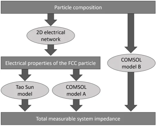
Several models are designed in order to estimate the impedance of FCC particles. An overview of the models that are used, is given in Fig. 2.7. This figure shows the inputs and outputs of each of the models. The 2D electrical network model uses the information about the particle composition, to calculate the average electrical proper-ties of the particle in each of the activity stages. This is used by both the Tao Sun model and COMSOL model A to calculate the total measurable system impedance. COMSOL model B will calculate the total measurable system impedance directly from the particle composition. Several models are used, as some models provide better un-derstanding while other models give more accurate results. Furthermore, each model gives slightly more information as different effects can be taken into account. The COMSOL models are much more time consuming and are therefore not suitable for parameter sweeps.
2D electrical network for particle properties
14 CHAPTER 2. THEORY &MODELLING
Fig. 2.7: Structure of the models that are used to calculate the impedance change as caused by FCC particles.
made for the resistivity and dielectric constant of the particle.
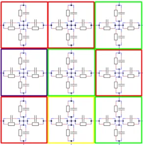
As the average electrical properties of the particles are unknown, the particle is divided into a large amount of sub-elements. Each of these elements represents a cluster of a pure molecule from Tab. 2.1, for instance Silicon dioxide (SiO2). The electrical properties of these pure molecules are known, therefore the resistance and capacitance of each cluster can be calculated. To make an equivalent circuit model, each cluster is given a square shape and is electrically connected to its direct neigh-bours.
To make the model as accurate as possible, as many clusters as possible should be used. Furthermore, these clusters should be small 3D structures which are connected to different clusters in all directions. However, due to limitations in calculation power, this is not possible. Therefore, the model that is used only shows material variation in 2 dimensions as shown in Fig. 2.8. Electrodes are placed above and below this particle.
In order to create an equivalent circuit model of the particle as shown in Fig. 2.8, the following steps are taken:
1. The material is divided into a 2D roster of 100 x 100 elements. The total amount of elements is therefore equal to 10000.
Fig. 2.8: Model of FCC particles as a collection of square clusters. The clusters show variation in the x and y direction, but not in the z-direction, making it a 2D model. Each colour represents a different material for the cluster.
a resistivity of 1013Ωm and a dielectric constant of 4.33 [49], [50].
3. Each of the elements is modelled with the circuit as shown in one of the squares in Fig. 2.9. The equivalent circuit model of each element thus consists of four resistors and four capacitors. This connects each element with the four nearest neighbours.
4. The resistivity and dielectric constants used to obtain the resistor and capacitor values of each element depend on the material that is assigned to each element. 5. The total particle is modelled as a square with dimensions of 80 micron. With these dimensions in combination with the resistivity and dielectric constant of each element, all the resistances and capacitances can be calculated. And a large network like Fig. 2.9 is formed.
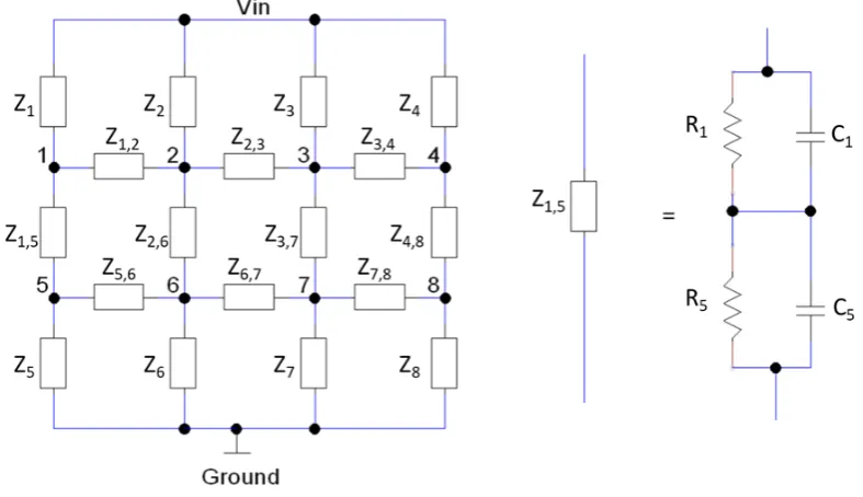
The next step is to solve this equivalent circuit model to obtain an average value for both the dielectric constant and resistivity of the model. This is done using the nodal voltage method.
In this method each point where multiple electrical components meet, is defined as a node, for instance pointVn in example the circuit of Fig. 2.10. The nodal voltage method starts by defining Kirchhoff’s current law for each node. This law indicates that the sum of all currents entering this node is equal to the sum of currents leaving the node. For each node, the equation with Kirchhoff’s current law can be written down, giving a set of equations. For node Vn of the example circuit, Kirchhoff’s current law becomes:
i1 =i2+i3. (2.11)
16 CHAPTER 2. THEORY &MODELLING
Fig. 2.9: Part of the equivalent circuit diagram used in the 2D electrical network. Each coloured square represents one element in the matrix of 100 x 100 x 1, which contains one specific material.
voltages and impedances:
Va−VN Z1
= VN −Vb
Z2
+ VN −Vc
Z3
. (2.12)
The number of nodes that the system contains, is equal to the amount of final equations as the one showed in Eq. 2.12. However, one of the nodes is set to be the reference, or ground node. For this node, the potential is set to zero and no equation is needed to describe its potential. The final equations that are obtained can be solved using linear algebra. This results in solving the voltages present at each node.
To avoid doing all the individual steps of the node voltage method for each node of the large electric network (containing 10000 nodes), some simplified rules can be used. These are explained in the following steps, which are based on literature [51].
6. The nodal voltage method matrix form uses the following equation as starting point:
Fig. 2.10: Example of approach in node voltage method. =
a1,1 a1,2 . . . a1,n a2,1 a2,2 . . . a2,n ... ... ... ... an,1 an,2 . . . an,n
· v1 v2 ... vn = z1 z2 ... zn , (2.14)
whereArepresents an impedance matrix which includes the impedances which connect all the nodes together [Ω],~unodes represents the voltages at each of the nodes [V] and ~zinput represents the known quantities due to voltage or current sources [A]. The indices from 1 till n are used to indicated the node of the element which is used. The number n indicates the total number of nodes, which is in this case equal to 10000. In the matrix,A, two indices are used to indicate a relation between these two nodes.
7. Some specific rules are used to obtain the impedance matrixA:
• When 2 nodes (i and j), as shown in Fig. 2.11 are connected, in the matrix at positionA(i,j) and A(j,i) the impedance is equal to − 1
Zij, where Zij is the
impedance of the circuit element that is placed between nodes i and j. • When 2 nodes are not connected directly by a circuit element in the
equiva-lent circuit model, in the matrix placeA(i,j) andA(j,i) the impedance is equal to 0.
• On the main diagonal the negative sum of each row is inserted. For the elements that are connected to either the input node (Vin) or the ground node, an additional element is added which is equal to 1
Zi, to include the
connection with the voltage source or ground.
8. The vector~zinputis equal to VZini for nodes i that are directly connected to the input voltage through an impedance with valueZi. As in the upper nodes in Fig. 2.11. 9. The voltages at each node can be obtained by:
~
18 CHAPTER 2. THEORY &MODELLING
Fig. 2.11: Equivalent circuit model of a system containing 2 x 4 nodes. In the ac-tual calculation a total of 100 x 100 elements is used. The impedance in-between the nodes represent impedances which combines the resis-tance and capaciresis-tance of multiple elements as shown as example for the impedanceZ1,5.
as the matrixAand vector~zinput are completely known.
In order to get the particle properties from the node potentials, some additional calculations are required. As in Fig. 2.11, all the elements on the top row are on one side connected to the input voltage. The total impedance of the complete system is equal to the source voltage divided by the source current. As the source voltage itself can be set and is therefore known, the current is the only requirement to find the impedance. By calculating all the individual currents through the elements on the top row (elements 1 until 4 for the circuit of Fig. 2.11) and the sum of these currents, the total current can be obtained. The total impedance should be separated into a resistance and a capacitance. This is done by first calculating the impedance for a DC input voltage, for which the capacitance is equal to zero: then the impedance is caused completely by the resistance itself. After that an AC voltage is chosen as input and the capacitance is calculated. From the resistance and capacitance, in combination with the dimensions of the element, the average resistivity and dielectric constant of the FCC particle can be obtained.
Tao Sun model: particle between electrodes
of the complete system of Fig. 2.1. To get from the particle properties to the system impedance that is finally measurable, the properties of the complete system should be taken into account, which includes the dimensioning and the material properties of the fluid. For a spherical particle in-between rectangular electrodes, a model to calculate the final impedance already exists in literature [8]. This model uses Maxwells mixture theory as starting point. This relates the electrical properties of the mixture with the individual properties of the solution and the spherical particle. The Maxwell Mixture equation is defined as:
˜
mix= ˜med
1 + 2Φ ˜fCM
1−Φ ˜fCM
, (2.16)
where f˜
CM represents the unitless complex Clausius Mossotti factor as defined in Eq. 2.17 and Φ the unitless volume ratio between the particle and the medium as
defined in Eq. 2.18.
˜
fCM =
˜
par−˜med
˜
par+ 2˜med
(2.17)
Φ = Vpar
Vmed
(2.18) In these equation, ˜mix, ˜med and ˜par represent the complex permittivities of the mixture, the medium and the particle respectively. A complex permittivity includes both the resistivity and the dielectric constant of an element:
˜
=− jσ
ω (2.19)
whererepresents the permittivity,σ the conductivity andωthe angular frequency. When using a shelled particle, the electrical properties of the particle itself depend on the individual inner and outer shell properties. This is defined as:
˜
par = ˜shl−
γ3+ 2K
γ3−K , (2.20)
whereK andγ are the following parameters:
K = ˜inn−˜shl ˜
inn+ 2˜shl
(2.21)
γ = R+d
d . (2.22)
20 CHAPTER 2. THEORY &MODELLING
Fig. 2.12: The equivalent circuit used to model a shelled particle in-between elec-trodes, modified from [8].
Furthermore, as explained in the paper of Sun, an equivalent circuit of the complete system can be made [8]. This equivalent circuit is shown in Fig. 2.12. This circuit can be used to analyse the individual contributions in more depth and to perform frequency analysis. The calculations of the resistor and capacitor elements is explained in detail in the paper of Sun [8].
In the model of the FCC particle, a total radius of 40 micron is used with an outer layer of 2 micron, as the metal mainly accumulates in this region. The resistivity and dielectric constants that are used, originate from the 2D electrical network model. Multiple simulations are performed to optimize the system parameters, like the channel dimensions and the choice of medium.
COMSOL simulations
Besides the previously described simulations which are analytical models, also some finite element models are made in COMSOL [52]. The advantage of using COMSOL, is that it allows for the calculation of the stray capacitance and makes it possible to change the particle position inside the channel. Furthermore, the results of the COM-SOL simulations are assumed to be more accurate. However, as these simulations are more time consuming, optimizing a certain parameter is easier to do using the previous described Matlab simulations.
Two different models are made in COMSOL. First of all, a shelled particle is mod-elled with homogeneous electrical properties. This particle has two dielectric con-stants, one for the shell and one for the inner part. In this model, the electrical proper-ties of the particle are taken from the 2D electrical network model. This model is thus an alternative for the analytical model using Maxwell’s mixture equations.
ma-Fig. 2.13: Simplified rendering of the COMSOL simulation showing the channel con-taining the electrodes in blue together with a shelled particle exactly posi-tioned in between these electrodes. The actual used structure in COMSOL contains a longer channel with thicker walls and includes the connections to the electrodes, which are left out for clarification purposes.
terials used for the channel walls are determined by cleanroom processes which will be explained in Chap. 3. The top and bottom channel walls will be mempax with a dielectric constant of 4.8 [53]. The side walls will be made from SU-8 with a dielectric constant of 4 [54].
In the second model that is made, the distribution of clusters in the particle is in-corporated into the model. This model can thus be seen as a alternative for the com-bination of the 2D electrical network model and the analytical model using Maxwell’s mixture equations. In this model a 3D cluster distribution is used with 200 by 200 by 200 elements. This distribution is shown in Fig. 2.14. This block is randomly given a value between 0 and 100. Hereafter, according to the percentages of each molecule that are present, each cluster is assigned to a molecule. For the simulations the same structure as in the first COMSOL model as shown in Fig. 2.13 is used. The electri-cal properties are however not homogeneous. The randomized cluster locations as shown in Fig. 2.14 is used to make the particle properties inhomogeneous. Metal ac-cumulation mainly occurs on the outer layer of the particle, which is incorporated into the model by assigning more clusters to the metal properties for the outer 2 micron.
capaci-22 CHAPTER 2. THEORY &MODELLING
Fig. 2.14: Image showing the randomized position of the clusters. The cube is divided into 200 x 200 x 200 elements which is given a random number between 0 and 100.
tance is hereafter calculated between the two electrodes. A spherical particle with a radius of 40 micron with one shell is placed in-between the electrodes and the dielec-tric properties of this particle are adapted according to the wanted situation.
2.3.2 Results and discussion
2D electrical network for particle properties
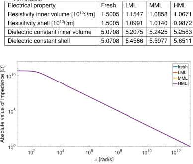
To obtain the average electrical properties of both the particle shell and inner volume in each metallization state, multiple sets of simulations are performed. The percentages used in the simulation relates to the specific situation and layer that is modelled and corresponds to Tab. 2.5. Because the outcome of each simulation is dependent on the exact positioning of the clusters, a total of 20 simulations are performed for each situ-ation and averaging of the results is performed. In the simulsitu-ations both the resistivity and the dielectric constant are calculated. The resistivity results of the simulations are shown in Fig. 2.15. The dielectric constant results are shown in Fig. 2.16. Both the average value and the standard deviation due to the cluster location differentiation are shown in these figures. A table summarizing the final resistivity and dielectric constant values for each state is shown in Tab. 2.6.
Fig. 2.15: Results of simulations for the resistivity of both the inner and outer volume. The height of the bars represents the average values and the error bars show the standard deviation due to the difference in location of the clusters between the simulations.
Fig. 2.16: Results of simulations for the dielectric constant of both the inner and outer volume. The height of the bars represents the average values and the error bars show the standard deviation due to the difference in location of the clusters between the simulations.
Tao Sun model: particle between electrodes
24 CHAPTER 2. THEORY &MODELLING
Tab. 2.6: Electrical properties of the inner volume and shell for the different metalliza-tion states.
Electrical property Fresh LML MML HML
Resistivity inner volume [1012Ωm] 1.5005 1.1547 1.0858 1.0671
Resisitivity shell [1012Ωm] 1.5005 1.0991 1.0140 0.9872
[image:32.595.83.473.103.433.2]Dielectric constant inner volume 5.0708 5.2075 5.2425 5.2583 Dielectric constant shell 5.0708 5.4566 5.5977 5.6511
Fig. 2.17: Absolute value of the impedance versus the system driving frequency. The impedance is plotted for the four stages of metal loading. However, as the impedance difference is small. the lines overlap.
liquid.
To check whether it is most suitable to use the particle resistance or dielectric constant, some simulations of the frequency response of the system are done. The channel dimensions as shown in Fig. 2.1 are equal to 300 micron for both the electrode width and length. The channel height which is the spacing between the electrodes is equal to 230 micron. The fluid that is used is demineralized water with a dielectric constant of 29.3 and the resistivity is 18.2M [Ωm] [55], [56].
A bode plot is made for the frequencies between 1 and 1013 radians/seconds and
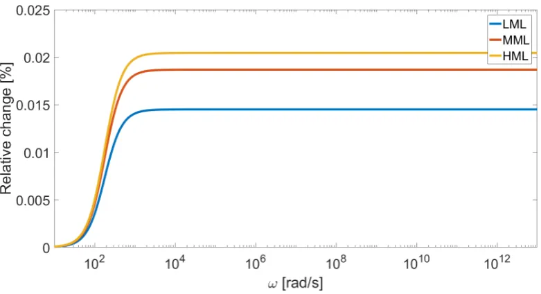
the result is shown in figure Fig. 2.17. The result is shown for each of the metal loading stage, but since the differences between these stages are small, this is not visible in the figure. Therefore another plot is made to show the percentual differences between each stage with respect to the fresh particles. This is shown in Fig. 2.18.
Fig. 2.18: The relative change in impedance between particles at which metal has accumulated (LML, MML or HML) and fresh particles without metal loading.
decade decrease of the impedance. What is not visible in this figure, is the electric double layer capacitance, which is present at the interface between the channel walls and the liquid. As the double layer is not of interest in this research and only present at low frequencies while using a conductive medium, the effects of the double layer capacitance are neglected [57].
Fig. 2.18 shows that the percentual change in impedance is largest at high fre-quencies. Using a different fluid with a resistivity closer to the particle resistivity would increase the relative change in this regime. However, the frequency at which the re-sistance of the system is dominant is already low and would only reduce when using a higher fluid resistivity. It is thus most suitable to use the capacitance and therefore the dielectric properties of the FCC particle.
Simulations showing the influence of the channel width and length are shown in App. A.1. This shows that to maximize the relative change in capacitance, the length and width of the electrodes should be as low as possible. However, the absolute change in capacitance remains constant for increasing electrode length and width.
The influence of the electrode spacing is shown in App. A.2. The simulations show that a smaller electrode spacing will result in both a larger relative change in capaci-tance as well as in a larger absolute change in capacicapaci-tance.
26 CHAPTER 2. THEORY &MODELLING
The capacitance that is measured, is not only affected by the metal content on FCC particles, but also by the size of the particle. In App. A.4, the effect of particle size is shown for multiple fluid dielectric constants. The simulations show that the effect of size variations is smaller whenever the dielectric constant of the fluid is close to the particle dielectric constant. The choice of dielectric constant can thus be used to reduce the effect of size differentiation of FCC particles.
Tab. 2.7: Capacitance of the system for the different metal accumulation stages sim-ulated using the Tao Sun model. Shown for using two different fluids which are of possible interest.
Capacitance [fF]
(change in capacitance with respect to a fresh particle [aF])
Medium (r) Fresh LML MML HML No particle
Demineralized water (29.3) 100.0217 (-) 100.0362 (14.5) 100.0403 (18.7) 100.0421 (20.5) 101.5152 (1493.5) Anisole (4.33) 15.0335
(-) 15.0404 (6.8) 15.0423 (8.8) 15.0431 (9.6) 15.0007 (32.8)
The capacitance value of the system for the different metal accumulation stages are shown in Tab. 2.7. This is shown for both demineralized water and anisole with dielectric constant of 29.3 and 4.33 respectively [55] [50] as these are two potentially interesting fluids. This table shows that the change in capacitance is highest when demi water is used. However, also the difference between no particle and a fresh particle is significantly higher for using demineralized water. This makes it easier to detect the FCC particles itself, but complicates finding the small difference in metal loading.
COMSOL
As explained in Sec. 2.3.1 two types of simulations are done using COMSOL. In the first set of simulations, the dielectric properties of the inner volume and the outer layer are homogeneous, and this is performed as alternative for the Tao Sun model. The system capacitance for the different metal accumulation stages are shown in Tab. 2.8. Comparing these results to Tab. 2.7 shows expected behaviour. In the COMSOL model the stray capacitance is taken into account, which greatly increases the total capacitance. As expected, the change in capacitance due to metal accumulation are comparable for the COMSOL model and the Tao Sun model. The results of these models are thus in agreement.
Tab. 2.8: Capacitance of the system for the different metal accumulation stages sim-ulated using the first COMSOL model. Shown for using two different fluids which are of possible interest.
Capacitance [fF]
(change in capacitance with respect to a fresh particle [aF])
Medium (r) Fresh LML MML HML No particle
Demineralized water (29.3) 363.5812 (-) 363.5958 (14.6) 363.6000 (18.8) 363.6018 (20.6) 365.0898 (1508.6) Anisole (4.33) 221.4779
(-) 221.4848 (6.9) 221.4868 (8.9) 221.4876 (9.7) 221.4460 (31.9)
Tab. 2.9: Position dependence of system impedance for fresh FCC particles in anisole moving 10, 20 and 50 micron in each direction. The x-direction is the direc-tion along the channel. The y-direcdirec-tion is towards the wall of the channel where the electrodes are located. The z-direction is towards the other wall of the channel
Capacitance [fF] (change in capacitance w.r.t center position) [aF]
Movement direction 0µm 10µm 25µm 50µm
x 221.4779 (-) 221.4781 (0.2) 221.4778 (0.1) 221.4774 (0.5) y 221.4779 (-) 221.4785 (0.6) 221.4798 (1.9) 221.4813 (3.4) z 221.4779 (-) 221.4779 (0.0) 221.4780 (0.1) 221.4775 (0.4)
position dependence of the detected capacitance is largest when the particle moves towards one of the electrodes. This capacitance change is smaller than the expected change in capacitance due to metal loading as seen in Tab. 2.8. It can however still have a significant influence on the experimental results.
The second COMSOL model directly incorporates the randomized distribution of molecules. For this model again the capacitance in the different metal accumulation stages are simulated and shown in Tab. 2.10. The total capacitance is as expected in the same range as the first COMSOL model. The change in capacitance however shows a quite significant difference. In this second model, the step between fresh and LML particles is much higher than any of the other steps and is also significantly higher compared to the first COMSOL model.
The cause of this difference might be due to the large number of total elements that is used in the second COMSOL model. The first COMSOL model uses the results of the 2D electrical network which uses in total 10 thousand elements, while the second model uses 80 Million elements. Furthermore, the 2D electrical network model might not be completely accurate due to the simplifications that are made in making the equivalent circuit model.
28 CHAPTER 2. THEORY &MODELLING
Tab. 2.10: Capacitance of the system for the different metal accumulation stages sim-ulated using the second COMSOL model. Shown for using two different fluids which are of possible interest.
Capacitance [fF]
(change in capacitance with respect to a fresh particle [aF])
Medium (r) Fresh LML MML HML No particle
Demineralized water (29.3) 363.6668 (-) 363.6915 (24.7) 363.6950 (28.2) 363.6958 (29.0) 365.0898 (1423.0) Anisole (4.33) 221.5167
(-) 221.5269 (10.2) 221.5283 (11.6) 221.5287 (12.0) 221.4460 (70.7)
particles and particles where metal has accumulated. This difference is expected to be between 14.5-29aF for using demineralized water and between 7-12 aF for using anisole. Depending on the amount of metal which has accumulated on the particle.
2.4 Microfluidics
To detect the FCC particles in a continuous way, microfluidics is used. Microfluidics has proven to be very effective in sensing applications [58]. It is therefore being used extensively in combination with impedance spectroscopy [59]–[61]. By flowing the particles one after the other through the chip, the throughput of measuring is greatly increased, while it is still possible to analyse each of the particles individually.
The most important considerations of microfluidics are the choice of medium and the flow that is created. The medium choice is partly made based on the electrical properties, for which the relevance is explained in Sec. 2.3. Furthermore, The fluid density, viscosity and interaction with the channel walls and the particle are also of rel-evance. For instance, the fluid should not react with the channel walls or the particles. The flow that is created within the channel will be important for the measurements that are performed. Although a faster flow of particles increases the potential through-put of the device, the particle should not pass the electrodes with too high velocities, otherwise measurements can not be performed accurately. This is partly caused by the limited sample rate which is used, but also due to filtering which is used to greatly reduce the noise that is measured. This filtering will also remove any fast changes in impedance introduced by particles moving with high speed. A trade-off should there-fore be made between the speed of the particles and the amount of filtering.
Fig. 2.19: Flow profile in a rectangular channel, modified from [64]
depends on Reynolds number:
Re= DHvρ
µ , (2.23)
WhereReis the unitless Reynolds number, DH is the hydraulic diameter in [m],v is the average velocity of the fluid in [m/s], ρ the density of the fluid in [kg/m3] and µ
is the dynamic viscosity in [Pa s] [62]. The hydraulic diameter of a square channel is defined as:
DH =
4wh
2(w+h), (2.24)
wherew is the width of the channel in [m] and hthe height in [m] [62]. Whenever Reynolds number is smaller than 2100, laminar flow is obtained [63]. To ensure that laminar flow is created, the channel dimensions, the medium and the flow speed that are used should be taken into consideration.
For movement of the medium through the channel, a syringe pump will be used. With this pump, the amount of flow per time unit can be set, which can be used to calculate the velocity of the fluid. For laminar flow, the flow profile that is created by the syringe pump will look like Fig. 2.19 [64], where flow will be largest in the exact middle of the channel and will reduce towards the channel walls.
The movement of FCC particles inside the channel is caused by two forces, drag forces and gravitational forces. As the particle will most likely have a higher density compared to fluid, gravitational forces will act on this particle. The gravity force acting on the particles is described in Eq. 2.25 [65].
FGp = (ρs−ρf)g πd3
6 (2.25)
30 CHAPTER 2. THEORY &MODELLING
of the particle in [m]. The difference in density of the particle and medium will there-fore determine the sedimentation speed due to gravity. When the channel is placed horizontally, the particles will sink to the bottom of the channel. Placing the channel vertically is another possibility. The direction of the gravitational forces can then either be in the same or opposite direction to the flow that is created. This will have an effect on the velocity with which the particles passes the electrode.
The second force is the drag force due to the difference in movement of the medium and the particle. As flow is created inside the channel, the medium will move with a certain velocity. This movement will cause the particle to be dragged along the channel. For fluids with low Reynolds number, Stokes drag will be exerted on the particle, for which the force is shown in Eq. 2.26 [66].
FD = 3πµvreld (2.26)
WhereFD is the drag force in [N],µthe dynamic viscosity in [Pa s],vrel the relative velocity of the fluid with respect to the particle in [m/s] anddthe diameter of the particle in [m].
Design
In this chapter the complete design of the experimental set-up is discussed. The design choices that are made are based on literature, experience and on the models as discussed in Chap. 2. In the first section, only the design of a microfluidic chip is discussed. Hereafter, the complete measurement set-up is explained.
3.1 Microfluidic chip design
A simplified drawing of the designed microfluidic chip is shown in Fig. 3.1. The design contains three inlets which are used for flow focus. Furthermore, two sets of electrodes are included, which allows for differential measuring.
Fig. 3.1: Schematic image of the design of the microfluidic chip used in the sensing of FCC activity
32 CHAPTER3. DESIGN
3.1.1 Particle position dependence
Due to the anisotropy in the electric field as generated, caused by the stray field in-troduced at the edges of the electrodes, the effect which the particle has on the final impedance is dependent on the exact position of the particle. This is also shown in the simulation results of Tab. 2.8. To reduce this effect, some features are added into the design, which will be discussed next.
Flow focus
Flow focus is added to ensure that all particles will cross the electrode at approximately the same position. A simple way to include flow focus is by using two extra inlets besides the particle inlet as shown in Fig. 3.1 [67], [68]. These inlets, combined with the particle inlet with a certain angle, hereby allow for focussing of particles in the centre of the channel. The design will thus only focus the particles position in one dimension.
Ground planes
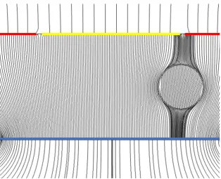
Another method to reduce the position dependence of the measured capacitance is the addition of ground planes. This method counters the direct cause of the position dependence, which is the non-uniform electric field due to edge effects of capaci-tors [69]. By adding some grounding planes around the electrode, the electric field becomes more uniform. This is made visible in Fig. 3.2. In Fig. 3.2a the electric field between the channel is shown without the addition of ground planes. In Fig. 3.2b, the ground planes are included and the electric field is shown again. This shows that, around the position of the particle which is indicated, the uniformity of the electric field is increased by the addition of ground planes. The location of the ground planes in the design is shown in Fig. 3.3.
Besides the improvement of the uniformity of the electric field, the grounding elec-trodes are also added to shield the sensitive elecelec-trodes. Shielding reduces coupling between the system and noise sources that are present around the set-up [70]. With-out shielding, the electrodes and the wires of the system could act as an antenna and pick up signals from the surrounding. The grounded electrodes create a barrier for the electric field lines from the noisy surrounding. These field lines will therefore no longer reach the sensitive circuit elements, hereby significantly reducing the amount of noise as present in the system.
3.1.2 Differential measuring
(a) Electric field inside the channel without the addition of groundplanes.
(b)Electric field inside the channel with ground-planes included.
Fig. 3.2: Comparison of the electric field generated inside the channel, without and with added ground planes. In the figures, the yellow line represent the top electrode, the blue line the bottom electrode and the red lines the added ground electrodes.
To be able to only measure this capacitance change introduced by the FCC particle, a differential measurement is performed. For this differential measurement, two identical capacitors are used as shown in Fig. 3.1. The capacitance detection system can be adapted to only measure the difference between these capacitor values:
Cmeas =C1−C2. (3.1)
Whenever no particle is located between both of the capacitors, only the medium will be present. Because both the dimensions and the dielectric constants of both sets of electrodes are identical, the measured capacitance should be zero. Whenever a FCC particle is present between the electrodes of C1, the capacitance of this
ca-pacitor will change, due to the dielectric properties of the particle, which is different from the medium dielectric constant. One of the advantages of differential measuring is the reduction of parasitic effects [71]. Since the parasitic capacitance should be identical for both capacitance, the parasitic effects will almost completely be cancelled out. Furthermore, also the influence of changes over time, for instance changes in temperature, will be reduced as the change is equal for both capacitorsC1 andC2.
3.1.3 Design considerations
34 CHAPTER3. DESIGN
Fig. 3.3: Simplified image of the masks used in the fabrication of the microfluidic chip. In cyan the mask for the channel is shown, the grey mask shows the bottom electrodes and the light yellow mask shows the top electrodes.
Tab. 3.1: Summary of the design choices that are made in the microfluidic chip design.
Parameter Value
Electrode length 300µm
Electrode width 300µm
Electrode spacing 230µm
Distance between sensing capacitors 1000µm
Medium choice Anisole
Medium dielectric constant 4.33 Medium resistivity 1013Ωm
Medium viscosity 0.778-1.52 cP
Medium density 995.6 kg/m3
Device dimensions
The length and width of the electrode are both chosen to be 300µm. This value is
the result of a trade-off. For smaller dimensions, the relative change in capacitance created by the FCC particle is larger. However the absolute change will not become larger. Furthermore, smaller channel dimensions will increase the change of particle clogging and will reduce the time for which the particles are in between the electrodes. This is caused by the decreased length of the electrodes.
As found during modelling, the electrode spacing should be as small as possible to maximize the change in measured capacitance due to metal accumulation. Whenever the spacing is too small, there is an increased change of particle clogging. As trade-off, an electrode spacing is chosen to be230µm.
should however also not be too large, else small differences in temperature or fluid properties can arise. The value of1000µmis chosen as a trade-off.
Medium
The medium that is chosen is anisole. This choice is based mostly on the dielectric constant of 4.33 [50], [72]. Although the absolute change in capacitance caused by metal accumulation is smaller for anisole in comparison to demineralized water, as shown in Tab. 2.8 and Tab. 2.10, the effect of particle size differentiation is greatly reduced when using anisole, which is shown in App. A.4. The dielectric constant of the medium should be as close to the FCC particle dielectric constant to reduce the size effects. When using demineralized water, the effect of1µmradius differentiation would
increase the measured capacitance with 100aF which would completely overshadow the change in capacitance due to metal accumulation. For anisole the change in capacitance is lower than 2.5aF for a1µmradius differentiation.
Another relevant property of anisole is the resistivity, which is 1013Ωm [49]. This
resistance is high enough for the capacitance to be dominant, even at low frequencies. The viscosity of anisole is 1.52 centipoise at 15 degrees Celsius and 0.778 cen-tipoise at 30 deg Celsius and therefore similar to the viscosity of water [73]. The density of anisole is 995.6 kg/m3 and is thus also very similar to water [73].
3.2 Measurement set-up design
An overview of the measurement set-up used in the detection of the FCC particle ac-tivity is shown in Fig. 3.4. This design makes use of a lock-in architecture similar to the one used by Wei [19]. From the options of impedance detection as given in Sec. 2.1.2, the lock-in architecture was chosen for several reasons. First of all, the measurements using the lock-in amplifier are fast and sensitive, due to the high frequency and small bandwidth at which the measurement can be performed [13], [14], [74]. Furthermore, the set-up is relatively easy to build and it is possible to incorporate differential mea-surements. The complete set-up is divided into several elements, which are discussed next.
3.2.1 Function generation
36 CHAPTER3. DESIGN
Fig. 3.4: Overview of the measurement set-up design using a lock-in architecture.
this node will only be dependent on the difference in the two capacitances. The current through this node will thus be defined by:
Iout =Isig+Iref =jωVinCsig−jωVinCref =jωVin(Csig −Cref). (3.2) Due to imperfections in the fabrication of the device, the capacitances Csig and Cref will not be exactly the same. This will result in an offset of the output current of the microfluidic device. To counter this, the amplitude with which both capacitors are driven can be adjusted.
For the measurement frequency a value of 300 kHzis used. At this frequency, the
capacitance of the system is dominant with the used medium of anisole.
3.2.2 Charge amplifier
In order to measure the capacitance difference of the microfluidic device, the current which is the output of the system should first be converted into a voltage. This is done using a simple charge amplifier. The output of this amplifier is formulated as:
Vamp =−Iout
1
1
Ramp +jωCamp
. (3.3)
The value of the resistorRamp is chosen to be 1MΩ, which is relatively high, such that the amplifying behaviour is dominated by the capacitor. The output of the amplifier then becomes as:
Vamp =−Iout
1
jωCamp
. (3.4)
the lock-in-amplifier indicated as:
Vamp =jωVin(Cref −Csig)
1
jωCamp
=Vin
Cref −Csig Camp
. (3.5)
These calculations assume a perfect operational amplifier with infinite gain. In reality, this is however not the case. Therefore, some noise is generated by the reading circuit:
Vno2 =VnA2
1 + Cp
Camp 2
+InR2 1 jωCF
, (3.6)
where Vno is the generated noise [V], VnA the voltage noise at the input of the operational amplifier [V],Cp is the parasitic capacitance as indicated in Fig. 3.4 [F] and InR is the thermal noise density of the amplifier resistance Ramp [A]. To minimize the noise, an amplifier should be chosen with minimum input noise density. Furthermore, the parasitic capacitanceCp should be as small as possible.
The capacitor used in the amplification circuit has a value of 3.3pF. This value is chosen as a trade-off between signal and noise amplification and based on experi-ence. Choosing lower values would result in higher signal amplification. However, the noise that is present would also increase which is not wanted.
3.2.3 Lock-in amplifier
In order to perform high accuracy measurements of the output voltage of the charge amplifier, a lock-in amplifier is used. This device is capable of measuring at a specific frequency, hereby removing the noise that is present on other frequencies. The lock-in amplifier measures the amplitude of the signal Vamp at the specific frequency of the input signal as explained in Sec. 2.1.2. The output of the lock-in amplifier are an in-phase and out-of in-phase voltage representing the amplitude of the measured voltage (Vamp) at the specific frequency. Only the in-phase output of the lock-in amplifier is of interest, as this represents voltage as indicated in Eq. 3.5. The out-of phase voltage of the lock-in amplifier represents the resistance of the electrodes of the microfluidic device.
38 CHAPTER3. DESIGN
3.2.4 Shielding compartment
As explained in Sec. 3.1.1 ground planes are added to the device in order to shield the sensitive electrodes from noisy signals around the set-up. For the same reason, all the sensitive element of the system are placed in a grounded box. This box contains two compartments, one for the microfluidic device and one for the charge amplifier. The currents that run through the conductors in these sections are very small and therefore extremely sensitive to noise. The other segments are less sensitive to noise and therefore not included in the grounded box.
3.2.5 Remaining set-up elements
A camera is used during measurements to get a size-estimation of the particles. The camera is zoomed in to the electrode elements of the chip and checks whether the peaks from the lock-in architecture are corresponding to a single particle. When clus-ters or dirt passes by the chip instead, the data is ignored.
Materials & methods
This chapter first discusses the materials that are used to perform the experiments. Hereafter, the section methods discusses the fabrication of the microfluidic chip and the plan of action of the performed experiments.
4.1 Materials
The materials that are used can be subdivided into fluids, particles, measurement equipment and software. These will be discussed in this section.
4.1.1 Fluids
The experiments were performed using two different fluids, demineralized water and anisole. The demineralized water is obtained from the Elga PurelabR Flex providing
water with a resistivity of 18.2Ω[75]. Anisole is obtained from Sigmaaldrich [76].
4.1.2 Particles
In the experiments, two types of particles are used: polystyrene particles and FCC par-ticles. Plain organic 80 micron polystyrene particles where obtained from microspheres-nanospheres [77]. The different metallization stages of FCC particles where obtained by density sorting into 4 categories: fresh, LML, MML and HML [1], [78]. In the exper-iments, only the fresh and HML stages where used.
4.1.3 Equipment
The signal generation and the lock in amplifier functionality are performed by the HF2IS Impedance Spectroscope. The impedance spectroscope is capable of gener-ating two anti-phase signals, while simultaneously measuring the system output with high accuracy [79]. A NEMESYS syringe pump from Cetoni GMBH is used with one
40 CHAPTER4. MATERIALS &METHODS
base module and three 290N modules are used [80]. As power supply the Delta elec-tronics Dual power supply E018-0.6D is used. For the video capture, the point grey grashopper 3, gs3-u3-23s6m-c is used [81]. The Schott KL1600 LED is used as light source [82]. The microfluidic chip is placed in a side-connect chipholder designed by micronit [83]. For the current amplifying circuit the OPA 2107 is used as opera-tional amplifier [84]. For the cyclic voltammetry, the sp-300 potentiostat by biologic is used [85].
4.1.4 Software
Modelling is done using Matlab R2016a and COMSOL multiphysics 5.3 [52], [86]. To control the syringe pump, the software neMESYS UserInterface is used [80]. For video capture, the program grey flycapture2 is used [81]. Data analysis is done using Matlab R2016a and ImageJ [86], [87]. Th program to control the potentiostat is EC-LAB V11.16 [88].
4.2 Methods
4.2.1 Chip fabrication
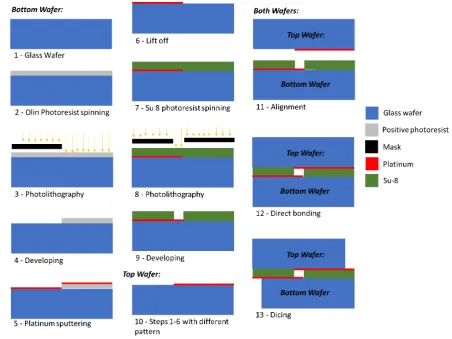
The microfluidic chip is fabricated using standard microfabrication processes in the MESA+ Nanolab cleanroom facilities. The design of the chip is based on the available technology and previous work. A detailed process flow is included in App. B. The masks that were used in this process are shown in App. C.
The general production steps are summarized in Fig. 4.1. As starting point of the manufacturing process, a Borofloat glass wafer is used. First, electrodes have to be deposited on top of this wafer, as done in steps 1-6. To be able to pattern the metallic layer, the lift-off process is used. This requires that, before the metal is deposited, first a layer of Olin photoresist is deposited. This layer is then patterned using photo-lithography by the EV620 Mask aligner. After development the patterns are present in the photoresist layer. On top of this layer the metal can be deposited by sputtering using the Tcoathy. Lift-off will then ensure the patterning of the deposited electrodes. These steps are done for both the top and bottom wafer, with a different pattern for each wafer.