Article
Role of MOSFETs Transconductance Parameters and
Threshold Voltage in CMOS Inverter Behavior in DC
Mode
Milaim Zabeli1, Nebi Caka2, Myzafere Limani2 and Qamil Kabashi1,*
1 Department of Engineering Informatics, Faculty of Mechanical and Computer Engineering ([email protected])
2 Department of Electronics, Faculty of Electrical and Computer Engineering ([email protected], [email protected])
* Correspondence: [email protected]; Tel.: +377-44-244-630
Abstract:The objective of this paper is to research the impact of electrical and physical parameters that characterize the complementary MOSFET transistors (NMOS and PMOS transistors) in the CMOS inverter for static mode of operation. In addition to this, the paper also aims at exploring the directives that are to be followed during the design phase of the CMOS inverters that enable designers to design the CMOS inverters with the best possible performance, depending on operation conditions. The CMOS inverter designed with the best possible features also enables the designing of the CMOS logic circuits with the best possible performance, according to the operation conditions and designers’ requirements.
Keywords: CMOS inverter; NMOS transistor; PMOS transistor; voltage transfer characteristic (VTC), threshold voltage; voltage critical value; noise margins; NMOS transconductance parameter; PMOS transconductance parameter
1. Introduction
CMOS logic circuits represent the family of logic circuits which are the most popular technology for the implementation of digital circuits, or digital systems. The small dimensions, low power of dissipation and ease of fabrication enable extremely high levels of integration (or circuits packing densities) in digital systems [1-5].
By noise margins, CMOS technology is the dominant of all the IC technologies available for digital circuits design. The fundamental circuit of CMOS logic circuit is the CMOS inverter. Electrical and physical parameters that characterize the complementary MOS transistors (or complementary MOSFET transistors) determine the behavior of CMOS inverter, as for static conditions of operation, as well as dynamic conditions of operation [6-9].
The CMOS inverter consists of two complementary MOS transistors (of an enhancement-type NMOS transistor and an enhancement-type PMOS transistor, because the enhancement-type of MOSFETs have high performance on depletion- type of MOSFETs), interconnected as in Figure 1 [6,10].
The NMOS transistor is called pull-down transistor, while the PMOS transistor is called pull-up transistor [11]. Complementary MOS transistors in the CMOS inverter operates in complementary mode depending on voltage level applied to the input terminal (to the gates of MOS transistors). In the CMOS inverter, the contribution of both MOS transistors is equal to the circuit operation
characteristics, therefore both transistors are considered as driver transistors. By circuit topology for input high voltage (high level), the NMOS transistor drives (pulls down) the output node while the PMOS transistor acts as the load (nonlinear resistor), and for input low voltage (low level) the PMOS transistor drives (pulls up) the output node while the NMOS acts as load [6,7,12].
It’s very important that the CMOS inverter has the static power of dissipation nearly zero, when the subthreshold conductions and leakage currents are neglected [7,12-15].
Figure 1. The structure of the CMOS inverter which contains two complementary enhancement-type MOS
transistors.
2. The role of the complementary MOSFET (NMOS and PMOS) transistors parameters in characteristic properties of the CMOS inverters
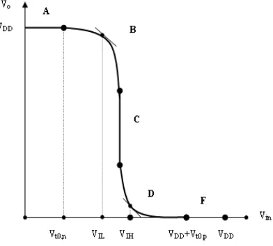
The behavior of the CMOS inverter for static conditions of operation is described by the voltage transfer characteristic (VTC), and for dynamic operation conditions is described by the time response during switching conductions [6,7]. The typical VTC characteristic of the CMOS inverter is shown as in Figure 2.
In the CMOS inverter, the NMOS transistor and PMOS transistor can be treated as a switch which operates in complementary mode [12].
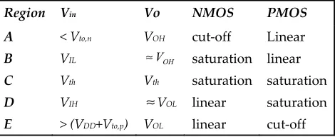
For construction of the VTC characteristic of the CMOS inverter, five different combinations of operation modes of the NMOS and PMOS transistors should be examined, which are the results of the various ratios of the input voltage levels and the output voltage levels. Operation modes of complementary MOS transistors within particular regions of the VTC characteristic are presented in Table 1.
Table 1. Operation modes of complementary MOS transistors (NMOS and PMOS transistors)
Region Vin Vo NMOS PMOS A
B C D E
< Vto,n VIL Vth VIH
> (VDD+Vto,p) VOH
OH
V
≈ Vth
≈
VOL VOL cut-off saturation saturation linear linear Linear linear saturation saturation cut-offThe characteristic properties that characterize the VTC characteristic are some voltage critical values at the input and output terminal of the CMOS inverter, as: VOH, VOL, VIL, VIH, Vth [3], [4].
VOH – output high voltage when output level is a logic “1” (high logic level), VOL – output low voltage when output level is a logic “0” (low logic level), VIL – maximum input voltage which can be interpreted as a logic “0”, VIL – minimum input voltage which can be interpreted as a logic “1”.
The voltage critical values at input and output of the CMOS inverter are determined by using combinations of operation regions (operation modes) of the NMOS transistor and the PMOS transistor, depending on the level of the output voltage values relative to the voltage values at the input of the CMOS inverter.
The critical value of output voltage VOH can be calculated by using the A region of VTC‘s, when the NMOS transistor operates in the cut-off mode, while the PMOS transistor operates in the linear mode, and after calculation will have voltage level of:
V
OH=
V
DD(1)
when
VDD – power supply voltage (source voltage).
By using the B region of the VTC characteristic, the definition for VIL critical value (the smaller
r n to r DD p to o IL
k
V
k
V
V
V
V
+
+
−
−
=
1
|
|
2
, ,(2) 2 , 0 2 , 0 ,
0
)
(
)
(
)
(
in t p in DD t p r in t no
V
V
V
V
V
k
V
V
V
=
−
+
−
−
−
−
(3)when
Vt0,n – the threshold voltage of the NMOS transistor, Vt0,p – the threshold voltage of the PMOS transistor,
kr – the transconductance parameters ratio of the NMOS and the PMOS transistors, Vin – input voltage.
p p n n p n
r
k
W
L
L
W
k
k
k
k
)
/
(
)
/
(
' '=
=
(4)kn – transconductance parameter of the NMOS transistor, kp – tranconductance parameter of the PMOS transistor,
'
n
k
- process transconductance parameter of the NMOS transistor,'
p
k - process transconductance parameter of the PMOS transistor,
W – channel width of the MOS transistor, L – channel length of the MOS transistor,
whereas indexes n and p indicate the NMOS and PMOS transistor.
The body effect of NMOS and PMOS transistor is not present in the CMOS inverter, because VSB of both transistors is zero. This will have to be taken into consideration in other types of MOS inverters, as in NMOS inverter, when it will influence the threshold voltage of NMOS and PMOS transistors, as well as the VTC shape of inverters.
Also, by using the definition for obtaining the expression for input voltage critical value VIH (the
larger of the two input voltage values at which the slope of the VTC characteristic becomes dVo/dVin = -1), and by using D region in VTC characteristic of CMOS inverter, and operation modes of the NMOS, and the PMOS transistors according to Table 1, we can obtain the expressions for the critical voltage value VIH and the output voltage Vo, as:
(
)
r n to o r p to DD IHk
V
V
k
V
V
V
+
+
+
+
=
1
2
, , (5) 2 , 0 2 , 0 ,0 ) ( ) 1/ ( )
( in t n in t n r in DD t p
o V V V V k V V V
V = − − − − − − (6)
(
)
r p to DD r n to
th
k
V
V
k
V
V
1
1
1
, ,
+
+
+
=
(7)The low output critical voltage value VOL is calculated using the E region of VTC characteristic, when the NMOS transistor operates in linear mode and the PMOS transistor operates in cut-off mode, resulting in:
V
OL=
0
V
(8)The critical input and output voltage values are also determinative to the noise margins values which characterize CMOS inverter for two logic levels (NML and NMH) in static condition of
operation (steady state). The noise margins for two logic levels are expressed as:
ML IL OL
N
=
V
−
V
(9)
N
MH=
V
OH−
V
IH (10)From the expressions of the input voltage critical values (VIL and VIH) and the output voltage critical values (VOL, VOH) achieved above, impact on these characteristic voltage values will have: the values of the power supply voltage (source voltage), the values of the threshold voltage of the complementary MOS transistors, as well as the values of transconductance parameters which characterize the complementary MOS transistors.
Relaying on fabrication processes advances of MOS transistors, it is possible that electrical and physical parameters which characterize MOS transistors can be controlled during fabrication process [1,3,6]. Therefore, we will examine the impact of these parameters on the particular magnitudes that characterize the CMOS inverter and based on them, can be defined the routes which lead to the design of the CMOS inverter with favorable performance according to the operation conditions and digital circuits based on CMOS logic [1,9,15-17].
3. Results and Discussion
The dependence of the input voltage critical value VIL on the ratio of MOS transistors
Figure 3. The dependence of input voltage critical value VIL on ratio of MOS transistor transconductance parameters (the ratio of NMOS transconductance parameters on PMOS transconductance parameters) kr for two different values of NMOS threshold voltage (Vt0,n), when threshold voltage of PMOS transistor has a constant value of Vt0,p = - 0.5V.
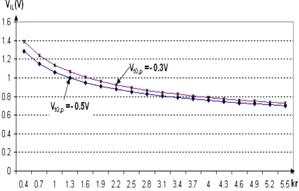
In Figure 4 is shown the dependence of input voltage critical value VIL on the ratio of MOS transistor transconductance parameters for a case when threshold voltage of PMOS transistor has two different values (parametric values), whereas the NMOS transistor threshold voltage remains constant.
Figure 4. The dependence of input voltage critical value VIL on the ratio of MOS transistor transconductance parameters kr for two different values of PMOS threshold voltage (Vt0,p), when threshold voltage of NMOS transistor has constant value of Vt0,n = 0.5V.
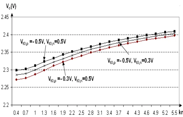
Figure 5. Influence of MOS transistor transconductance parameters ratio (kr) on output voltage value Vo, when the input terminal of CMOS inverter is biased by voltage Vin = VIL, for several parametric values of complementary MOS transistor threshold voltage.
From the results presented in Figures 3 and 4 for the input voltage critical value VIL, we note that as the higher the value of the transconductance parameter ratio of complementary MOS transistors is, the low critical value of input voltage VIL will decrease. For higher values of the NMOS threshold voltage, the input voltage critical value VIL, will shift to higher values. Also, for the higher value of the absolute value of PMOS transistor threshold voltage, the input voltage critical value VIL will shift to the lower values.
The results presented in Figure 5 show that when the MOS transconductance parameters ratio have higher value, the output voltage value Vo will have higher values, when the input terminal is
biased by Vin= VIL (or by input low voltage critical value). Also, the impact on output voltage value Vo will have likewise the values of MOS transistors threshold voltage, but this impact is less important compared to the ratio of MOS transistors transconductance parameters. However for lower values of the complementary MOS transconductace parameters ratio, the impact of threshold voltage of complementary MOS transistors will be more significant.
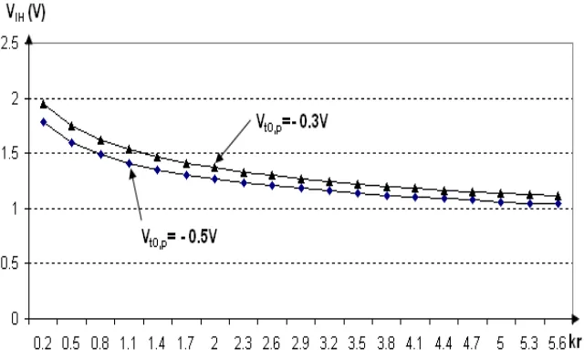
The impact of the MOS transistor transconductance parameters ratio, the MOS transistor threshold voltage values in input voltage critical value VIH (high critical value of input voltage) are
Figure 6. The dependence of the voltage critical value VIH on MOS transistors transconductance parameters ratio kr for two parametric values of NMOS transistor threshold voltage, when PMOS transistor threshold voltage remains constant Vt0,p = - 0.5 V.
Figure 7. The dependence of voltage critical value VIH on MOS transistors transconductance parameters ratio kr
for two parametric values of PMOS transistor threshold voltage, when NMOS transistor threshold voltage remains constant Vt0,n = 0.5V.
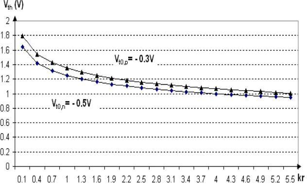
The MOS transistors transconductance parameters ratio and the values of the MOS transistors threshold voltage will have impact on the CMOS inverter characteristic value which is called the CMOS threshold voltage value (or switching threshold).
In Figures 8 and 9 is shown the impact of the MOS transistors transconductance parameters ratio that constitute CMOS inverter on the CMOS inverter threshold voltage value Vth for several parametric
values of complementary MOS transistors threshold voltage (NMOS and PMOS threshold voltage).
Figure 8. The impact of the transconductance parameters ratio (kr) of MOS transistors (NMOS and PMOS) on value of the CMOS inverter threshold voltage (on value of CMOS inverter switching threshold voltage) for two different values of the NMOS threshold voltage, when Vt0,p = - 0.5 V and source voltage VDD = 2.5 V.
Figure 9. The impact of the transconductance parameters ratio (kr) of MOS transistors (NMOS and PMOS) on value of the CMOS inverter threshold voltage Vth (on value of CMOS inverter switching threshold voltage) for two different values of the PMOS threshold voltage, when Vt0,n = 0.5V and VDD = 2.5 V.
of the CMOS threshold voltage Vth would increase in value, especially the impact will be more
prominent for greater values of the transconductance parameters ratio kr (kn > kp). While when the threshold voltage of the PMOS transistor has a higher value by absolute value, the value of the CMOS threshold voltage Vth will be decreased, and this decreasing will be more significant when the
transconductance parameter ratio kr has lower values (kp < kn).
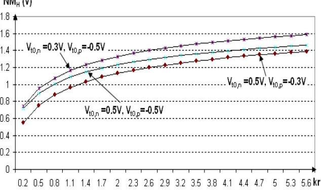
The immunity of CMOS inverter on unwanted signals is expressed through the noise margins for both logical levels (for low level and for high level). The parameters that characterize the complementary MOS transistors in a CMOS inverter determine the noise margins level for both logical levels. The dependence of noise margins (NM) on the complementary MOS transistors transconductance parameters ratio, for several parametric values of MOS transistors threshold voltages in both logic levels are shown in Figures 10 and 11.
Figure 10. The dependence of the noise margins for low logic level NML on complementary MOS transistors transconductance parameters ratio kr, for three cases of different MOS transistor threshold voltage (NMOS and PMOS transistors), when VDD = 2.5 V.
The results in Figure 10 indicate that the higher values of the MOS transconductance parameters ratio kr, noise margin for the low level will be lower. For the lower value of the NMOS transistor threshold voltage (Vt0,n), the level of noise margins NML (noise margins for low level) will decrease,
resulting in the significant reduction in the band of higher values of the transconductance parameter ratio kr. Also, the smaller the PMOS transistor threshold voltage value (Vt0, p)by absolute value, the level of noise margins NML (noise margins for low level) will increase, especially in the range of small
Figure 11. The dependence of the noise margins for high logic level NMH on complementary MOS transistors transconductance parameters ratio kr, for three cases of different MOS transistor threshold voltage (NMOS and PMOS transistors), when VDD = 2.5 V.
The level of noise margins NMH (noise margins for high level) will increase when the MOS
transconductance parameter ratio is designed to be higher, Figure 11. For smaller value of NMOS threshold voltage, the noise margin for high level NMH will increase especially in the range of higher values of the transconductance parameter kr. While the lower value of PMOS threshold voltage by absolute value (Vt0,p), the level of noise margins NMH will decrease, especially with significant impact
in the range of low values of the transconductane parameter ratio kr.
By matching the values of complementary MOS transconductance parameters and values of their threshold voltage, the CMOS inverter can be designed with higher performance, depending on the requirements of designer that dictate operation conditions. For CMOS inverter with matched parameters as: kn= kp and Vt0, n=| Vt0, p| will be achieved that the noise margin to be equal to both logic levels and the value of the threshold voltage of the CMOS inverter will be half of voltage source Vth = VDD/2. The CMOS inverter which possesses these features is called symmetric inverter and it must satisfy the condition:
(
)
(
)
(
(
)
)
1 / / 2.5 / / n p symetricn ox n
n n n
p n
p p ox p p p
k k
C W L W L
k W W
k C W L W L L L
μ μ μ μ = = = ⇔ ≈ (11)
and although the MOS transistors built by equal length of channel defined by lithographic process, it appears that:
( )
W
p≈
2
.
5
( )
W
n) (12)and PMOS transistors as much as possible, which enable the design of the CMOS inverter with acceptable performance. The impact of NMOS and PMOS transistor parameters in shape of the VTC characteristic is shown in Figure 12.
Figure 12. The impact of complementary MOS transistors channel length ratio (Wn/Wp) on VTC shape, when Ln =Lp, Vt0,n = |Vt0,p|= 0.5 V and VDD = 2.5 V.
From the VTC shape presented in Figure 12 we can see the impact of the channel width (respectively the ratio of the transconductance parameter kr) in the shape of VTC characteristic VTC, resulting in displacement of the VTC's left or right, depending on the channels widths ratio, and reflecting in the characteristic values of VTC's.
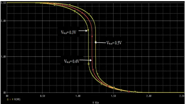
When the value of NMOS transistor threshold voltage increases, and the PMOS transistor threshold voltage remains unchanged, the VTC characteristic of CMOS inverter shall shift to the right from the lower value of the NMOS threshold voltage (Vt0.n), which is reflected in the voltage critical
values, Figure 13.
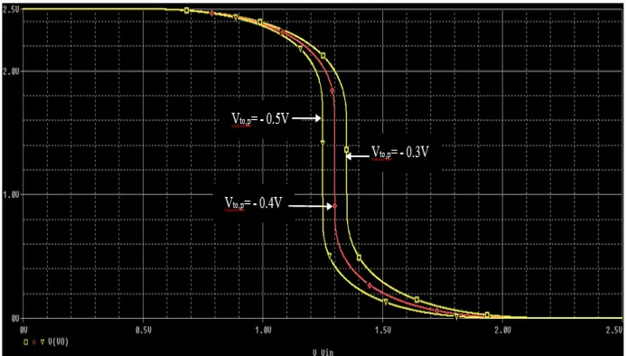
In Figure 14 is shown the impact of the PMOS transistor threshold voltage value in VTC shape of CMOS inverter when the NMOS transistor threshold voltage has a fixed value. When the PMOS transistor threshold voltage has lower value by an absolute value, then the CMOS inverter VTC) will shift to the right from the larger value.
Figure 14. The impact of PMOS transistor threshold voltage (Vt0,p) on CMOS inverter VTC shape, when NMOS transistor threshold voltage value is Vt0,n = 0.5 V, and transistors have identical dimensions.
According to the shapes of VTC characteristic of the CMOS inverter presented in Figures 12-14 the slope of VTC characteristic in particular regions is indicted. It’s very important that the slope of VTC characteristic in region named by C is same in all cases, which differs for other types of MOS inverters.
4. Conclusions
If during the design phase of the CMOS inverter, the threshold voltage values of complementary MOS transistors (with the threshold voltage of NMOS (Vt0,n) and PMOS transistor (Vt0,p)) and the ratio of complementary MOS transistors transconductance parameters (the ratio between transconductance parameters of NMOS transistor (kn) and PMOS transistor (kp), kr = kn/kp) are controlled, or matched, the CMOS inverter can be designed with high performance as for static conditions of operation, as well as for dynamic conditions of operations, depending on the designer requirements and operating conditions.
As for the output voltage critical values VOL and VOH(or for high and low logic level at output), the transconductance parameter ratio of the complementary CMOS transistors (kr) and the complementary MOS transistor threshold voltages (Vt0.n and Vt0,p) don’t have impact, but their values are determined by zero volt (ground voltage) and source voltage value (VDD).
For the higher values of complementary MOS transistors transconductance parameters ratio (kr), lower value of the NMOS transistor threshold voltage (Vt0,n) and higher value by absolute value of the PMOS transistor threshold voltage (Vt0.p), the input voltage critical value VIH will decrease, whereas noise margin for high level NMH will increase.
As for the output voltage value Vo when Vin = VIL, for the higher values of complementary MOS transistors transconductance parameters ratio (kr), lower value of the NMOS transistor threshold voltage (Vt0,n) and higher
References:
1. Lundager, K.; Zeinali, B.; Tohidi, M.; Madsen, J.K.; Moradi, F.Low Power Design for Future Wearable
and Implantable Devices. J. Low Power Electron. Appl.2016, 6(4), 20; doi:10.3390/jlpea6040020.
2. Pal, A. Low-Power VLSI Circuits and Systems; Springer: New Delhi, India, 2015.
3. Plummer, J.D.; Deal, M.D.; Griffin, P.B. Silicon VLSI Technology: Fundamentals, Practice and Modeling; Pearson
Education, New Delhi, India, 2009.
4. Zant, P.V. Microchip Fabrication: A Practical Guide to Semiconductor Processing, 6th ed.; McGraw-Hill
Education, 2014.
5. Salman, E.; Friedman, E.G. High Performance Integrated Circuit Design; McGraw-Hill Publisher, NY, USA,
2012.
6. Kang, S.; Leblebici, Y. CMOS Digital Integrated Circuits, 4th ed.; McGraw-Hill, 2016. 7. Sedra, A.; Smith, K.C. Microelectronic Circuits, 7th ed.; Oxford University Press, 2015.
8. Caka, N.; Zabeli, M.; Limani, M.; Kabashi, Q. Role of driver and load transistor (MOSFET) parameters on pseudo-NMOS logic design. WSEAS Transactions on Circuits and Systems, 2010, 8, 557-566.
9. Karl, E.; Wang, Y.; Ng; Y.G.; Guo, Zh.; Hamzaoglu, F.; Meterelliyoz, M.; John, K.; Bhattacharya, U.; Zhang, K.; Mistry, K.; Bohr, M. A 4.6 GHz 162 Mb SRAM Design in 22 nm Tri-Gate CMOS Technology with Integrated, Read and Write Assist Circuitry. IEEE J. Solid-State Circuits,2013, 48, 150–158.
10. Taur, Y.; Ning, T.H. Fundamentals of Modern VLSI Devices, 2nd ed.; Cambridge University Press, 2016. 11. Rani, L.V.; Latha, M.M. Pass Transistor-Based Pull-Up/Pull-Down Insertion Technique for Leakage Power
Optimization in CMOS VLSI Circuits. Circuits, System. Signal Process.2016, 4139–4152, doi: 10.1007/s00034-016-0257-z.
12. Baker, R.J. CMOS Circuit Design, Layout, and Simulation, 3rd ed.; IEEE Press, 2010.
13. Weste, N.H.E.; Harris, D.M. CMOS VLSI Design: A Circuits and System Perspective, 4th ed.; Addison-Wesley, 2011.
14. Zhang, H.; Huang, M.; Zhang, Y.; Li, X.; Yoshihara, T. A nano-power switched-capacitor voltage reference using body effect in MOSFETs for application in subthreshold LSI. In Proceedings of the IEEE International Conference of Electron Devices and Solid-State Circuits (EDSSC), Hong Kong, China, 3–5 June 2013.
15. Uddin M.J.; Nordin A.N.; Reaz M. B. I.; Bhuiyan M.A.S. A CMOS power splitter for 2, 45 GHz ISM band RFID rider in 0,18 µm CMOS technology.Tehnicki vjesnik. 2013, 20(1), 125-129.