Surface Engineering for Microsensing
130
0
0
Full text
(2) Surface Engineering for Microsensing Author. Minati Luca. Tutors. Prof. Claudio Migliaresi Dr. Giorgio Speranza.
(3) A mio padre.
(4) CONTENTS. 1. Thesis Outline. 4. Chapter 1: Introduction. 34 Chapter 2: Experimental section. 44 Chapter 3: Functionalization of carbon nanotubes. 62 Chapter 4: Synthesis and characterization of carbon nanotubes films. decorated with gold nanoparticles. 87 Chapter 5: Optical properties of carbon nanotubes. 94 Chapter 6: X-ray photoelectron spectroscopy studies on gold metal. nanoclusters/amorphous carbon composite. 114 Chapter 7: Characterization of gold nanoclusters synthesized on. carbon nanotubes film: evaluation of the size distributions by means of X-ray photoelectron spectroscopy. 123 Conclusions and perspective.
(5) Thesis Outline. Chapter 1: Introduction In this chapter the topic of carbon nanotubes and gold nanoparticles is briefly introduced, and the current state of the art is overviewed. The main chemical and physical properties of carbon nanotubes as well as synthesis and functionalization procedures are reported. Regarding gold nanoparticles some general considerations are reported about the optical and chemical properties. At the end of the chapter some analytic techniques used in this Thesis are presented.. Chapter 2: Experimental section This chapter starts with a brief overview of the synthesis procedure used in each chapter. At the end of the chapter a brief description of the X-ray photoelectron spectroscopy experimental setup are reported, as well as of the principal instruments used in the Thesis work for the sample characterization.. Chapter 3: Functionalization of carbon nanotubes This chapter describes the characterization procedure and the functionalization processes of multi walled carbon nanotubes. The most relevant results were the high yield of the oxidation of the carbon nanotubes and the high efficiency of grafting of thiol functional groups on the carbon nanotubes surface. This last was verified with different characterization methods. Finally, the interaction of the thiol functionalized carbon nanotubes with gold films and gold nanoparticles was investigated.. 1.
(6) Chapter 4: Synthesis and characterization of carbon nanotubes films decorated with gold nanoparticles In this chapter the carbon nanotubes were deposited on metallic substrates by using an external electric field to induce orientation and migration of the carbon nanotubes in solution toward a chemically modified electrode. The efficiency of the procedure was verified with scanning electron microscopy and atomic force microscopy. The carbon nanotubes films were further decorated with gold nanoparticles deposited by adsorption. The samples were tested as surface enhanced Raman spectroscopy substrate for the detection of anions in solution.. Chapter 5: optical properties of carbon nanotubes In this chapter the optical luminescence of functionalized carbon nanotubes and carbon nanotubes gold nanoparticle hybrids are presented. In particular, the carbon nanotubes decorated with gold nanoparticles show a drastic increase of the photoluminescence in solution respect to the carbon nanotubes without the gold nanoparticles. The effect was investigated with the optical spectroscopy and an interpretation of the experimental results is given.. Chapter 6: X-ray photoelectron spectroscopy studies on gold metal nanoclusters/amorphous carbon composite In this chapter, the characterizations results on gold nanoclusters embedded in a carbon matrix are presented. In particular, the X-ray photoelectron spectroscopy characterization is used to analyze the chemical and structural composition of small gold nanoparticles deposited on carbon. Using a theoretical approach combined to experimental data the size distribution of gold NPs a-C/Au samples is estimated by line-shape analysis of the Au 4f photoemission spectrum. The calculated size distributions are in good agreement with that calculated with different techniques.. 2.
(7) Chapter 7: Characterization of Gold nanoclusters synthesized on carbon nanotubes film: evaluation of the size distributions by means of X-ray photoelectron spectroscopy In this chapter gold nanoclusters are directly synthesized on thiol functionalized carbon nanotubes film and characterized by means of X-ray photoelectron spectroscopy. Detailed analysis of the Au 4f core line using the methodology presented in the previous chapter is used to study the chemical modifications occurring on the substrate, as well as to obtain information on the nanocluster size distribution after each reducing treatments.. 3.
(8) CHAPTER 1 1.1 Introduction to carbon nanotubes Carbon, because of its electronic configuration is a really versatile element. Pure carbon can assume a few allotropic forms because the four valence electrons can organize with different spatial orientation on the basis of their hybridization. Diamond and graphite are examples of sp3 and sp2 hybridizations (upper left and right in figure 1.1) leading to distinct optical, electrical and mechanical properties. The organization of s and p electrons in sp2 hybrids enables carbon atoms to generate other unique structures. The C60 buckyball (lower left in figure 1.1) was discovered in 1985 by Kroto et al [1]. The carbon nanotubes (lower right in figure 1.1) were discovered in 1991 by Iijima [2]. These carbon structures that couple quantum effects, lower dimensionality and the unique properties of graphene [3, 4] have generated intense research in the material science.. Figure 1.1. Models of carbon allotropes. From top left: diamond, graphite, nanotube, C60 buckyball (staff.science.uva.nl) 4.
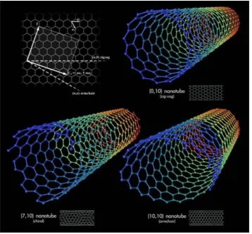
(9) 1.1.1 Structure of nanotubes and characterization methods The structure of nanotubes originates from that of graphite. Here electrons are organized in wavefunctions lying in a plane and along directions making angles of 120°. This causes the carbon atoms to arrange in hexagons in two-dimensional sheets overlapped each other in a stack leading to the crystalline structure of graphite. The single sheet of graphite is called graphene. A single-walled nanotubes (SWNTs) can be ideally obtained by rolling up a graphene sheet. When more sheets are rolled up together, the nanotube is called multi-walled. They are composed by concentric cylinders of graphene layers. Multi-walled nanotubes dimensions are typically larger than SWNTs which diameter are in the range of few nanometers. There are plenty of techniques to characterize CNT on the basis of the information desired: the scanning electron microscope (SEM), scanning tunneling microscope (STM), atomic force microscope (AFM) and transmission electron microscopy (TEM) to characterize their structure. XPS, FTIR, to study the chemistry behind CNT functionalization and processing. CNTs can be produced in many ways, either as a chemical reaction (chemical vapor deposition) or a physical process (arc discharge and laser ablation). Each individual nanotube can be uniquely identified with three quantities: nanotube diameter, chirality and number of walls. These parameters will be briefly introduced in the following of this section, along with methods for their characterization.. Diameter. TEM is the best analytic technique to measure the carbon nanotubes diameter, but its use is limited to suspended nanotubes. AFM suffer from some problems related to the limited tip curvature that leads to an overestimation of the nanotubes diameters. Raman spectroscopy is another tool to measure small SWNTs. The radial breathing mode (RBM) phonons, where all carbon atoms oscillate radially with the same phase, generate a strong peak in Raman spectroscopy at around 200 cm-1. The peak position, being inversely proportional to tube diameter allows its estimation.. 5.
(10) Number of walls. The best analytic technique to discriminate between single and multi walled carbon nanotubes is TEM. On the other hands TEM require carbon nanotubes in suspensions. When nanotubes are integrated into devices however, they are typically sitting on substrates, making TEM unable to be used in these experiments.. Chirality. When the graphitic sheet is rolled up along the symmetry axis Z to form the CNT, the hexagons may be organized in a spiral mode. The chirality describes the inclination of the hexagon spiral along Z. Chirality is more difficult to probe because it comes from atomic scale details. STM has been shown to be the best technique to resolve the arrangement of carbon in SWNTs [5, 6] but it is rather complex and requires conductive substrates.. Figure 1.2. Scheme of the chirality for single-walled carbon nanotubes.. 6.
(11) Another possibility is to use Raman spectroscopy. When the diameter of a nanotube is small, a precise measurement of diameter can reveal also its chirality since there is one-to-one correspondence between these two quantities. The RBM peak positions in Raman can be used as the most accurate way to measure tube diameter and thus chirality [7].. Defects. STM is the best analyric technique to detect defects in SWNTs [8]. Another possibility is the Raman spectroscopy [9]. When defects are present in the carbon nanotubes, the D-band, typical around 1340 cm-1 in Raman spectroscopy appears. The presence of defects may lead to a change in the electronic band structure on the SWNT , leading to a modification of RBM peak magnitude.. 1.1.2 Properties of nanotubes and potential applications The unique electronic, mechanical and biological properties of the carbon nanotubes along with potential applications will be presented in this section. Besides them, the small size of nanotubes also leads to many unique advantages that will also be discussed.. Electronic properties. SWNTs have interesting electrical properties. These arise from quantization effects due to the reduction from a macroscopic three-dimensional system to one having one infinite dimension and the remaining two measurable on an atomic scale. SWNTs are made of graphene, which has high intrinsic electron mobility [4] due to the lack of lattice defects as compared to most other semiconductor materials. In SWNT situation is different. Their diameters are too small that the electron wave vectors along the circumferences are quantized leading to a series of sub-bands in the electronic structure. It also makes SWNTs either metallic or semiconducting depending on their chirality. SWNTs have remarkable electrical performances. Defect-free SWNTs can have mobility larger than 10.000 cm2V/S-1. The band structure and one dimensionality also make carbon nanotubes a unique optoelectronic material. The electron density of states in nanotubes has a number of singularities, associated with the onsets of sub. 7.
(12) bands (Van Hove singularity see figure 1.3). Therefore, nanotubes can be viewed as semiconductors with multiple bandgaps, which can efficiently absorb lights of a wide spectrum [10]. Thanks to the electronic structure CNT are luminescent in the UV, visible and the infrared regions, each of these transition are strictly related to band-band transitions. The first observation of intrinsic luminescence is due to O‘Connel et al. in nanotubes isolated in SDS aqueous micelles [11]. Since then, luminescence of SWCNTs has been confirmed by other groups for single self-suspended nanotubes grown between catalyst pillars by chemical vapor deposition technique [12]. Indeed, it is possible to observe SWCNTs luminescence at room temperature in various conditions as far as tubes are isolated.. Figure 1.3. (dI/dV)/(I/V) measure of the density of states versus V. The asymmetric peaks correspond to Van Hove singularities of the carbon nanotube. The left-inset displays the dI/dV data. The right inset is the calculated density of states (DOS) for a (16,0) tube.[6] Mechanical properties. The utility of nanotubes as the strongest or stiffest elements in nanoscale devices or composite materials remains a powerful motivation for the research in this area. The Young‘s modulus of nanotubes (~ 1TPa) is five times higher than that of steel [13]. The largest experimental value observed for MWNTs is about 60GPa [14]. In comparison, the tensile strength of steel is less than 1GPa. At the same time, CNTs are extremely light. 8.
(13) Chemical properties. Because of their molecular-scale size, carbon nanotubes are sensitive to environments. Defect-free SWNTs are chemically inert. SWNTs are ideal materials to make detectors that are capable to reach single-molecule level sensitivity [15]. Potential applications are not limited to sensors. SWNTs have large surface to volume ratio which makes them an interesting material as electrodes in electrochemistry [16]. The high stability of SWNTs renders them appealing as hydrogen storage candidates [17]. Finally, SWNTs has been used as carriers for cells drug delivery [18]. However, there are some concerns regarding the toxicity of SWNTs induced by the easy internalization in cells. Recent studies showed that SWNTs injected in mice could be excreted within a couple months [18] without any toxic effect.. 1.1.3 Nanotube Growth Methods Arc-discharge and laser ablation methods have been actively used in the past ten years for the nanotubes growth. They all involve sublimating graphite in a reduced atmosphere or rare (inert) gases, brought to temperatures above 3200°C that is the sublimation temperature of graphite and condensing the resulting vapour under a high temperature gradient.. Arc-Discharge and Laser Ablation. An arc discharge is generated between two graphite electrodes placed face to face in the machine‘s principal airtight chamber under a partial pressure of helium or argon. Arc-discharge is an excellent method for producing both high quality multi-walled nanotubes and single-walled nanotubes. MWNTs can be obtained by controlling the growth conditions such as the pressure of inert gas in the discharge chamber. [19] The laser ablation technique is rather similar to the arc method as it also consists of sublimating graphite in a reduced atmosphere and has been proven to lead to very similar structures to those obtained by the arc method. Ablation of a graphite target with a focused laser beam is realized in an inert atmosphere at low pressure [20]. The growth of high quality SWCNTs was achieved by Smalley and co-. 9.
(14) workers using a laser ablation method [21]. The method utilizes intense laser pulses to ablate a carbon target containing 0.5 atomic percent of nickel and cobalt. The target is placed in a tube-furnace heated to about 1200°C. During laser ablation, a flow of inert gas passes through the growth chamber to carry the grown nanotubes downstream to be collected on a cold finger.. Catalytic CVD Growth. Catalytic Chemical Vapor Deposition (CVD) processes make possible the growth of carbon filaments of various sizes and shapes at low temperature (≤1000 °C) from carbon-containing gaseous compounds, which decompose catalytically on transition-metal particles [22, 23]. CVD growth relies on the capability to provide the atoms needed to form the solid deposit from a gas source that decomposes under the action of temperature. The growth process involves heating a catalyst material to high temperatures in a tube furnace and flowing a hydrocarbon gas through the tube reactor for a period of time. Materials grown over the catalyst are collected upon cooling the system to room temperature. The key parameters in nanotubes CVD growth are the hydrocarbons, catalysts and growth temperature. The active catalytic species are typically transition-metal nanoparticles formed on a support material such as alumina. The general nanotube growth mechanism in a CVD process involves the dissociation of hydrocarbon molecules catalyzed by the transition metal and dissolution and saturation of carbon atoms in the metal nanoparticles. The precipitation of carbon from the saturated metal particle leads to the formation of tubular carbon solids in sp2 structure. Tubule formation is favored over other forms of carbon such as graphitic sheets with open edges.. 1.1.4 Carbon nanotubes modification Purification. A large problem with nanotube application is next to large-scale synthesis also the purification. The as-produced SWNT soot contains a lot of impurities. The main impurities in the soot are graphite sheets, amorphous carbon, metal catalyst and the smaller fullerenes.. 10.
(15) Purification may consist of controlled oxidation, by mean of chemical, [24] or plasma treatments [25]. Chemical oxidation, among the other purification systems, can create terminal and surface defects readily saturated by oxygen-containing functional groups such as, for example, -COOH allowing further functionalization. Refluxing in dilute nitric acid can be considered as a mild oxidation for CNTs, introducing the carboxylic acid groups only at those defects initially present on the carbon nanotubes. The atomic abundance of the carboxylic groups generated with this oxidant remains constant along with the treating time. The oxidation processes begin mainly with the oxidation of the initial defects that arise during the growth of the CNTs and are accompanied by processes that can be roughly divided into two steps: (1) the defect-generating step and (2) the defect-consuming step. Specifically, during the defect-generating step, the oxidation agents attack the carbon nanotubes skeleton and generate oxygen-containing functional groups such as -OH and –C=O. The rate of the reaction depends on the oxidants ability to generate -C-OH groups and to transform them into –C=O groups. During the defect-consuming step, the graphene structure of the tube is destroyed by the oxidation of the generated active sites. The defect-consuming step mostly counts on the ability of the oxidant to etch/destroy the graphite-like structure around the functional groups. The sulphuric and nitric acid mixture (normally 1:3 HNO3/H2SO4) is normally used to introduce a high amount of defect and functional groups in the carbon nanotubes [26], as well as to reduce the carbon nanotubes length.. Functionalization. Functionalization is based on making SWNTs more soluble than the impurities by attaching other groups to the tubes. Now it is easy to separate them from insoluble impurities, such as metal, with filtration. The lack of solubility and the difficult manipulation of carbon nanotubes cause some limitations to their use. Indeed, as-produced CNTs are insoluble in all organic solvents and aqueous solutions. This is the reason beyond the interest in investigating the CNT functionalization even before potential applications. It was demonstrated that CNTs could interact with different classes of compounds [27] forming supramolecular complexes or undergo regular chemical reactions. This makes them more soluble, so improving their integration into inorganic, organic, and biological systems. The main approaches for the modification of carbon nanotubes can be grouped into two 11.
(16) principal categories: (a) the covalent attachment of chemical groups through reactions onto the carbon nanotubes walls (b) the non-covalent adsorption of various functional molecules. The first class of CNT modifications, involving strong chemical bonds between tubes and interacting molecules, in its turn, can be roughly divided into two categories: a direct bond of functional groups to the graphitic surface and functionalization of CNTs by strong oxidizing agents to form carboxylic bonds.. Covalent functionalization on the carbon nanotubes backbone. SWNTs have been found to react when treated with molecular fluorine at temperatures between 150 and 600 °C [28]. Other examples include the interactions with anilines, [29] the reactions with nitrenes, carbenes and radicals. Moreover, an efficient method for obtaining covalent modified soluble CNTs was developed by Prato [30]. The most successful approach for the in situ generation of azomethine ylides is based on the decarboxylation of immonium salts derived from condensation of amino acids with aldehydes. The 1,3-dipolar cycloaddition of azomethine ylides was found to be very effective in the functionalization of CNTs. In principle, any moiety could be attached to the tubular network to generate a wide variety of functionalized CNTs.. Chemical functionalization of oxidized CNTs. The covalent functionalization of carbon nanotubes can be obtained by using functional groups grafted on the surface of the carbon nanotubes by acid treatment. The creation of terminal carbons in the shortening and purification process on nanotubes, which upon oxidation are converted to carboxylic acids, are ideal platforms for the functionalization of the carbon nanotubes [31, 32]. Activation of the carboxyl moieties with thionyl chloride and subsequent reaction with amines is one of the most used reaction. Figure 1.4 shows a typical functionalization procedure that, at last, conjugates SWCNTs with an amine. [33] Amide bond was the first strategy used, by Haddon to achieve soluble nanotubes [29]. By bonding long alkyl amines, CNTs that are insoluble in organic solvents becomes soluble in chloroform, dichloromethane and aromatic solvents. This result was the basis of many further analogous experiments. Water soluble MWCNTs were realized by Sun and co12.
(17) workers. substituting. the. terminal. alkyl. amine. with. the. aminopolymer. poly(propionylethylenimine-co-ethylenimine) (PPEI-EI).. CNT. H2SO4/HNO3. CNT-COOH CNT-COCl. CNT-COOH. SOCl2. R-NH2. CNT-COCl CNT-CONH-R. Figure 1.4. CNT functionalization with primary amine via thionyl chloride acylation.. Diimide-activated reactions. Concerning bio conjugation between carboxylic and amino groups, the most exploited reaction family involves the carbodiimides molecules. Carbodiimides are used to induce the formation of amide bonds between carboxylic groups and amine. There carbodiimides can be water-soluble and water-insoluble. The water-soluble ones are the most common choice for biochemical reactions. Water-insoluble carbodiimides, instead, are used frequently in peptide synthesis and other conjugations involving molecules soluble only in organic solvents. As an example 1-ethil-3-(3-dimethylaminopropyl) carbodiimide hydrochloride (EDC) is the most popular carbodiimide for use in biological field. Excess reagent and the by-product of the cross-linking reaction are both water-soluble and may be easily removed by dialysis or gel filtration [34]. Carbon nanotubes, with their –COOH induced groups, are frequently functionalized by means of diimide-activated amidation. It is an alternative and blander method respect to acyl halides functionalization, to bind CNTs to functionalized amine. Another kind of functionalization between the carboxylic groups of the CNTs and aminic groups was found by Liu and co-workers [26]. In this paper, he presented an amidation reaction mediated by dicyclohexylcarbodiimide (DCC) molecules in ethanol. Using this strategy, he was able to couple carboxylic functional groups of the carbon nanotubes with ammine groups of a short chain thiol forming thiol functionalized carbon nanotubes.. 13.
(18) Carbon Nanotubes Arrays. Well-aligned CNT structures are requested for potential CNT applications, such as field emission displays, field emission transistors, superhydrophobic surfaces, chemical sensors, and CNT reinforced. The first examples of aligned CNTs was produced by cutting thin slices of a CNT-polymer composite [35]. Controlled CNT arrays are usually synthesized by growing CNTs on catalyst (e.g. Fe, Ni, Co) pre-patterned substrates in a chemical vapor deposition (CVD) reactor [36] or by self-assembling functionalized CNTs on a substrate [26]. Concerning CVD, iron oxide nanoparticles were used to produce both SWCNTs and MWCNTs arrays. [40]. Even suspended, SWCNT networks were synthesized by contact printing of catalyst onto the tops of silicon pillars [36]. On the other hand, CNT arrays were manipulated with functionalized CNTs using the selfassembling strategy. Oxidized CNTs obtained by acid treatment were self-assembled on silver [37] and Fe coated silicon substrates exploiting the interactions between carboxylic groups of CNTs and substrates surface [38]. Finally, thiol functionalized shortened CNTs were selfassembled on gold substrates [39].. 14.
(19) 1.2 Introduction to metal clusters Although nanoparticle research appears to be a quite modern subject, metal clusters were already put into application in antiquity. Noble metals, for example, played an important role in the coloring of glasses and ceramics. One of the most famous examples is the roman Lycurgus Cup, dated between 5th and 4th century B.C. It transmits ruby-red and reflects green light (figure 1.5). Examination with modern equipment revealed gold and silver nanoparticles present in the cup [41]. At that time, of course, the existence of nanoparticles was unknown and it was until 1857 that Faraday found the role of small particles on coloring when he dissolved gold in a colloidal suspension and observed the same deep ruby color.. Figure 1.5. The Lycurgus Cup (4th Century B.C) is ruby red in transmitted light and green in reflected light, due to the presence of gold colloids.. 1.2.1 Metal cluster electronic structure Nanoparticles are scientifically interesting nowadays because they represent a kind of transition between atom and bulk solid. The electronic configuration of nanosized particles is known to be different from the bulk state [42]. As electron configuration defines most of the. 15.
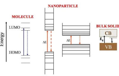
(20) bulk physical and chemical nature, nanoparticles can be expected to show different behavior respect to the macroscopic systems counterparts. For example, metals exhibit a transition from metal to semiconductor when the size is reduced. A simple model, which takes into account the decrease of the density of states at the Fermi level in small clusters, can be used to explain this behavior. In big clusters or bulk material individual electronic states form band structures typical of metals (figure 1.6). For small particles, the band structure is composed by discrete levels corresponding to a transition to atomic structure due to the spatial confinement of conduction electrons. If the energetic difference between the levels exceeds the values for thermal energies, the cluster shows nonmetallic behavior. The metal-nonmetal transition size can be estimated by the Kubo criterion: [43] δ ≈ 2Ef /3NaZ ≥ kBT. (1). where Ef the width of the conduction band, NaZ is the number of cluster atoms and z their valence. For gold (z = 1) the result is: δ ≈ 8eV/NA. This implies that the semiconductive nature of metal clusters can be observed at room temperature only for very small particles. This model does not take into account changes of the electronic configuration due to the quantization effect but it gives an upper size limit for quantization effects. It also illustrates that metal-to-insulator transitions are an intrinsic feature arising from the decrease of the particle size. The thermodynamic properties of small particle are known to be different to that of the bulk material. For example, nanoclusters exhibit a lowered melting point respect to the bulk counterparts. [44] Nanoparticles are interesting for a variety of electronic applications, such as Single-Electron Transistors (SET) [45, 46] and as electronic contacts to molecules [47]. The investigation of optical properties of individual clusters is a very active field [48, 49, 50]. Catalytic activity can also be strongly enhanced using nanosized metals [51].. 16.
(21) Figure 1.6. Representation scheme of the density of states near the Fermi level for single molecules, nanoparticles and bulk solid structure.. Much effort is put in the examination of such finite-size effects, as they promise to be useful for future application. Different chemical and physical techniques have been developed to grow nanoparticles [52, 53 54]. Contrary to physical methods, wet chemical procedures usually have the advantage of yielding macroscopic amounts of particles. This procedure also allows to synthesize passivated particles surrounded by a shell of organic molecules, preventing particle aggregation. [55, 56] The particle growth normally leads to a distribution of cluster sizes. Physical methods may provide size-selected particles, but with a much lower yields. The above discussions make it obvious that a detailed knowledge of nanoparticle properties and their dependence on the cluster environment (like passivating molecules) is of primary interest in order to build nanoscale structures.. 17.
(22) 1.2.2 Optical properties of metal nanoparticles. Theories of Photon-Plasmon Interaction. This paragraph introduces the theories that describe the photon-plasmon interaction. The surface plasmon wavefunction, defined as oscillations of the conduction band electrons in a film, is induced by an interaction between a photon and electrons. The maximum transfer of energy occurs when the surface reflectivity of the metal decreases, an indication of the photon energy transfer to the surface to the formation of plasmon waves. This condition is fulfilled within a certain range of wavelengths. The outcome of this phenomenon is surface plasmon resonance. To describe the excitation of the surface plasmon oscillation, the Mie theory is commonly used.. Exciting Surface Plasmons. The aim is to determine the proper parameters to excite surface plasmons in order to characterize its behavior. To generate a surface plasmon, an evanescent wave is produced. This wave penetrates the metallic surface and induces an oscillation of the electrons at the metal-dielectric surface causing the surface plasmon resonance (SPR). SPR occurs when the modulus of the wave vector k of the surface plasmon equals the modulus of wave vector k of the incident light. A second equation takes into account the spatial directions of these two vectors:. k light. = k SP. n p sin( θ ). 2π λ. ≈. 2π λP. ε nr n 2 s ε nr + n 2 s. (2). where nP is the refractive index of the prism coupler, εnr is the real portion of the dielectric constant of the metal, λ is the incident wavelength, λP is the wavelength of the surface plasmon, and θ is the angle of incidence.. 18.
(23) The refractive index, dielectric constant, and the wavelength of the surface plasmon are constants that depend on the type of sample used; the angle and wavelength of incidence are the variable components that alter the surface plasmon resonance. Since the dielectric constant of a metal is complex, the surface plasmon wave is also complex. In addition, the dielectric function depends heavily on the wavelength of the incident light, influencing the overall surface plasmon resonance. For metallic particles, the excitation of surface plasmons also depends on the polarizability of that particle. Polarizability is the relative tendency of a charge distribution, like the electron cloud of an atom or molecule, to be distorted from its normal shape by an external electric field. In general, the excitation of a system involves the light scattering. The scattering is a process based on up to two photons which occurs when incident light is transmitted through a system. A portion of the light leaves the system with unchanged frequency (or energy) while the remaining portion is scattered. The intensity and polarization of the scattered light depends on the observation direction. Therefore, the scattered light has characteristics associated not only with the incident source but also with new combinations of frequencies generated from photon interactions.. Mie Theory. In 1908, researcher Gustav Mie developed a theory that mathematically describes the scattering of incident light by spherical particles. The Mie theory is a rigorous solution for the scattering intensity from a spherical, homogeneous and isotropic particle of any diameter d in a non-absorbing medium [57]. Mie began his mathematical description by applying spherical coordinates to Maxwell‘s equations with suitable boundary conditions and parameters such as the particle size, characteristics of the particle material and of the surrounding medium. For such kind of system, the solution describes the multipole oscillations for the extinction crosssection of nanoparticles [58]. Mie also determined that the scalar electromagnetic potentials associated with the particles could be derived from their electric and magnetic fields. Furthermore, his solution related the interaction of electromagnetic incident light and small spheres with the optical properties of bulk material, specifically the frequency-dependence of the material dielectric constant. [58] Let us consider nanoparticles that are much smaller than the wavelength of the incident light (r/λ<<1). In this case, according to the calculations from Mie, only the dipole oscillations are significant for the extinction cross-section: 19.
(24) σ est ( ω ) = 9. ω c. ε m 1 .5 V. ε 2 (ω ) [ε1 (ω ) + 2ε m ]. 2. + ε 2 (ω ). 2. (3). where V is the spherical volume (4π/3)r3, ω is the frequency of the incident light, c is the speed of light, and εm and ε(ω)=ε1(ω)+iε2(ω) are the dielectric constants of the surrounding medium and the material, respectively. Note that resonance is achieved when the conditions ε1(ω) = -2εm and ε2(ω) is independent on the angular frequency are fulfilled. [59] Equation 3 has been used to determine the absorption spectra of small metallic nanoparticles. The Mie‘s theory is then able to explain the red color associated with gold nanoparticles in aqueous solution. Mie‘s theory assumed low concentration and non-interacting nanoparticles systems. This assumption implies that the electric field generated by a single nanoparticle does not interact with that of other nanoparticles. If the particles distance becomes small, a change in the absorption wavelength occurs in the plasmon resonance and a secondary absorption peak, at longer wavelengths, is observed.. 1.2.3 Gold Nanoparticles Bulk gold is particularly appreciated for its low reactivity toward oxidation. It is infact defined noble metal. Although gold is the subject of one of the most ancient themes of investigation in science it is object of an exponentially increasing number of publications, especially in the context of emerging nanoscience and nanotechnology with nanoparticles and self-assembled monolayers (SAMs).. Synthesis. Among the conventional methods of synthesis of AuNPs by reduction of gold (III) derivatives, the most popular one for a long time has been that using citrate reduction of HAuCl4 in water, which was introduced by Turkevitch in 1951 [60]. It leads to AuNPs with diameter of around 20 nm. In 1973 Frens, [61] proposed to vary the ratio between the. 20.
(25) reducing/stabilizing agents (the trisodium citrate to gold ratio) to control the AuNPs size (between 10 and 147 nm).. Applications. As already mentioned, one of the properties, which can vary extremely as the size of the particle becomes very small, is its catalytic activity. At nanometer scale, this activity can depend on the geometric and electronic structure of the particle. For supported nanoparticles, the influence of the substrate should be also taken into account. The catalysis of noble metal nanoparticles became especially important at the end of the 1980´s as M. Haruta and coworkers discovered that gold nanoparticles can exhibit a high catalytic activity for reactions such as CO-oxidation, propylene epoxidation and other industrial reactions, specially at low temperature (about 200 K) [62]. Due to the sensitivity of noble metals to light gold nanoparticles have been used as drug carriers for biomedical applications [63]. For example, microcapsules filled with a drug, can be delivered directly to its target location within a cancer cell, avoiding undesired side effects of medications. In order to release the drug, these nanoparticles are introduced into together with a dye in microcapsules. The Au nanoparticles act as strong absorption centers so that a laser pulse leads to a local heating which breaks the capsules with release of their content. Many of these special properties are based on quantum confinement effects at nanometer scale. A simple explanation of this effect relates the material properties with the degree of freedom of electrons which in its turn depends on the nanoparticle size. AuNPs have been used to manipulate the selectivity between solutes in capillary electrophoresis. Therefore, the AuNPs serve as large surface area platforms for organofunctional groups that interact with the capillary surface, the analytes, or both. The apparent mobility of target analytes as well as the electro-osmotic flow could be altered, which leads to enhanced selectivity. [64] The use of AuNPs has also been extended to chip-based capillary electrophoresis devices, the AuNPs in the microchannels acting as a rectifier. Electromagnetic coupling effects with lithographically produced AuNPs were investigated by photon scanning tunneling microscopy. The surface plasmon propagation on microstructured metal thin films was examined in order to provide an interface between the nano-optical device and classical farfield optics. [65] The optical manipulation of particles on waveguide surfaces offers a controllable tool for application to particle sorting, sensing, and atomic mirrors. In this context, potassium-ion21.
(26) exchanged optical waveguides in glass for evanescent field propulsion of AuNPs were optimized. [66] Encapsulation techniques are currently used to reduce photo-oxidation in commercial devices. In particular, utilization of AuNPs in optoelectronic devices often enhances the optical and electrical properties as well as the stability, this technique effectively inhibits photoluminescence decay. [67]. 1.3 Characterization techniques Characterization and comprehension of material physical and chemical properties are of fundamental importance in order to evaluate their potentiality and to explain their responses during applications. In this thesis, characterization allows controlling CNT properties during production, purification and modification, as well as surfaces of all the carbon nanotubes employed in this work. A wide range of tools allows researchers to study carbon materials and their properties, although each of these techniques reveals only a portion of the full spectrum of characteristics. The following paragraph describes some of the techniques employed to characterize CNT and gold nanoparticles.. 1.3.1 Photoelectron spectroscopy X-ray photoelectron spectroscopy (XPS) is a quantitative spectroscopic technique that measures the elemental composition, empirical formula, chemical state and electronic state of the elements that exist within a material. It is based on the photoelectric effect, explained by A. Einstein in 1905 [68]. X-ray absorption by an atom in solid leads to emission of an electron either from deep core-levels (core lines) or from weakly bonded electrons (valence band). A fraction of these electrons escape into the vacuum system. The kinetic energy EK of the photoelectron is related to the energy of the photon hν by the following expression: EK =hν –EB. (4). where EB is the electron binding energy, h is the Planck constant and υ is the frequency of the radiation. The additional amount of energy that an electron needs to overcome the energy difference between the Fermi energy (Ef) and the vacuum energy (Evacuum) is known as work. 22.
(27) function of the sample (Φsample). Considering this additional energy, the kinetic energy (EK) that an electron has after leaving the sample, is given by: EK =hν−EB –Φsample. (5). Figure 1.7. Schematic energy diagram of X-ray photoemission.. Since the spectrometer possesses its own work function (Φspectrometer), the kinetic energy EK measured by the spectrometer is given by (see figure 1.7): EK=hν −EB –Φspectrometer. (6). One-electron approximation. The first approximation used to explain the single electron photoemission effect was given by Koopmans [69]. Using this approach, the binding energy of an electron is considered equal to the energy difference between initial state (atom with n electrons) and final state of the atom. 23.
(28) (atom with n-1 electrons). Therefore, the binding energy of this electron is equal to the orbital energy ε with the negative sign:. EB= Efinal(n-1) –Einitial(n) E = −ε. (7). This approximation, does not take into accounts the effects of surrounding electrons due to the positive hole created by the ejected photoelectron. This approximation of the photoemission effect implies that the rearrangement of the surrounding electrons around the atoms is neglected. Initial state effects. Although the core level binding energies of a given element are sufficiently unique to allow the precise identification, they are not fixed values. The electronic configuration is influenced deeply by chemical bonding. The electronegativity and oxidation state of the neighboring atoms can change the electronic configuration, with the appearance of shifts or modifications in the lineshape of the peaks [70]. Information from these shifts provides a quantitative method of chemical analysis. The ability to discriminate atoms with different chemical shifts is limited by the peak widths. Apart the instrumental resolution, the width of the photoemission peaks is determined by the lifetime of the positive core hole created by the photoemission process. Because of the nature of the screening process of the positive hole, the deeper the core hole, the higher are the numbers of de-excitation channels.. Final state effects. The core hole created by the photoemission has a polarizing effect on the surrounding electrons. The electronic response is referred to as relaxation. The system relaxation energy corresponds to the energy difference between the excited electron system that have loose an electron and the relaxation of the system. There are some differences depending on the material. In a bulk metal, the positive charged state created by the photoemission is completely shielded by the conduction electrons and the cores of neighboring atoms. For 24.
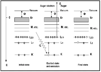
(29) isolated metal nanoparticles deposited on poorly conducting substrate [71], the number of conduction electrons and neighboring atoms is limited by the particle size and the positive hole can be screened less efficiently.. Auger Peaks. Figure 1.8 shows the sequence of events following the photoemission. The K level is show as being ionized by an hv radiation. Following the creation of a core hole in the K level, the atom relaxes by filling the hole via a transition from an outer level (L1). As a results the energy difference becomes available to eject a second electron (L2,3). In this Auger process illustrated in figure 1.8, the final state is a doubly ionized atom with core holes in the L1 and L2,3 shells. The energy of the ejected electron in the example of figure 1.8 is: EKL1L2,3 = EK – EL1 – EL2,3. (8). In general, the analysis of the Auger peaks can be used to detect elements. It is worth mentioning that Auger peaks always accompany XPS, but they usually rise with broader and more complex structure than photoemission peaks.. Figure 1.8. Schematic diagram of the Auger emission in solid. 25.
(30) Spin-orbit splitting. The total angular momentum of a single isolated electron is obtained by summing the electronic spin S and angular momenta L. For example in a 3d orbital, the total angular momentum J may assume two different values corresponding to J=L+S = 5/2 and J+L-S=3/2. These configurations give rise to two states characterized by different energies which give origin to the spin orbit splitting of the 3d core level. This splitting can be observed in the Ag 3d XPS spectrum. In this case, Ag 3d5/2 states are at lower binding energy than the state Ag3d3/2. For other orbitals like the s orbitals, the angular momentum L = 0. Therefore, for s core level there is not any splitting. These states are called singlet in XPS. In contrast, p, d, f orbitals with angular momentum equal to 1, 2, 3, show spin-orbit splitting.. 1.3.2 Electron microscopy In electron microscopy, the electrons interact with the atoms that make up the sample producing signals that contain information about the sample's surface topography, composition and other properties such as electrical conductivity. The signals result from interactions of the electron beam with atoms at or near the surface of the sample. In the most common or standard detection mode, secondary electron imaging or SEI, the SEM can produce very high-resolution images of a sample surface, revealing details about less than 15 nm in size. Scanning electron microscopy allows to image a rope of SWCNTs in a sample or to view the MWCNTs films [72], (figure 1.9) as well as to characterize surface morphology of other materials. Although the resolution does not allow imaging of individual SWCNT, it can be used, combined with other techniques, to determine the amount of impurities such as amorphous carbon or metal catalyst particles, which typically coexist with CNTs. SEM is also useful for analyzing carbon nanotubes decorated by gold nanoparticles as we see later on. Although SEM can be useful in imaging the MWCNTs, the transmission electron microscopy (TEM) is much more helpful for structural studies of carbon nanotubes. It allows to determine the number of walls in a MWCNT or to image the isolated SWCNTs residing inside a bundle. In addition, careful measurements of the tube diameters, as well as investigation of structural defects in CNTs are possible. An important benefit that comes with using electron microscopy techniques is the use of energy-dispersive X-ray diffraction (EDX).. 26.
(31) Figure 1.9. SEM pictures of CNT films [72].. Energy dispersive X-ray spectroscopy is an analytical technique used for the elemental analysis or chemical characterization of a sample. As a type of spectroscopy, it relies on the investigation of a sample through interactions between electromagnetic radiation and matter, analyzing x-rays emitted by the matter.. Figure 1.10. TEM micrograph showing the layered structure of a MWCNT.. 27.
(32) 1.3.3 Atomic force microscopy Scanning probe microscopies have been exploited to investigate the electrical and mechanical properties of individual nanostructures such as carbon nanotubes. The atomic force microscopy (AFM) is a very high-resolution type of scanning probe microscopy. In SPM, images are obtained by measuring changes in the magnitude of the interaction between the probe and the specimen surface as the surface is scanned beneath the probe. Hence, the resolution will depend on the sharpness of the probe tip, and the accuracy with which the sample can be positioned relative to the probe.. Figure 1.11. Schematic representation of the atomic force microscope.. The system is composed by a micro-fabricated, extremely sharp spike mounted on the end of a cantilever. The second fundamental component of an AFM is the scanning mechanism, an accurate positioning system done by means of a piezoelectric transducer. Typically, the deflection is measured using a laser spot reflected from the top surface of the cantilever into an array of photodiodes. 1.3.4 Raman spectroscopy Raman spectroscopy is a spectroscopic technique used to study vibrational, rotational, and other low-frequency modes in a system. Typically, a monochromatic light is employed,. 28.
(33) usually from a laser in the visible, near infrared, or near ultraviolet range. For carbon nanotubes, several Raman modes have been identified as disorder-induced modes, such as D mode (1350 cm−1) and D‘ mode (1620 cm−1). The Raman spectrum (figure 1.12) of carbon structure contains two main bands: The G-mode is the ―in-plane‖ symmetry E2g mode whereas the D-band (1200–1300 cm-1), attributed to the A1g (sp3-bonded) stretching mode resulting from the presence of a disordered structure or lattice defects in the graphite structure. The intensity ratio of the G-line (IG) to the D-line (ID) in Raman spectra is a useful parameter to evaluate the quality of carbon materials. A high ID/IG ratio is indicative of the presence of defects inside the carbon layer.. Figure 1.12. Typical Raman spectrum of a MWCNT .[73] The D* mode is the second-order overtone mode and appears between 2500 and 2900 cm-1. It is assigned to the first overtone of the D mode and often called D*mode. Moreover, contrary to the D mode, the D* intensity increases with the decreasing of the lattice disorder [73]. Out of all Raman modes observed in the spectra of SWNTs, the radial breathing modes. are unique to SWNTs. They appear between 150 cm-1 and 300 cm-1 from the elastically scattered laser line. It corresponds to the vibration of the carbon atoms in the radial direction, as if the tube is breathing. An important point about these modes is the fact that the energy of these vibrational modes depends on the diameter of the SWNTs.. 29.
(34) 1.3.5 Fourier transform infrared spectroscopy Infrared spectroscopy is widely used in both research and industry as a simple and reliable technique for measurement, quality control and dynamic measurement. FTIR can give both qualitative and quantitative information, although it is most important and characteristic use is in the identification of chemical bonds. Adsorptions are typically collected in medium infrared region (4000 – 400 cm-1) where functional groups undergo to a clean dipolar moment change as a consequence of a vibrational or a rotational motion [74]. FTIR application in CNT field is therefore not particularly useful in pristine material characterization, but can provide interesting information about functional groups grafting on the tubes after functionalization processes.. 1.3.6 UV-vis spectroscopy UV-vis spectroscopy has recently been reported as an important tool for characterizing the electronic band structure and quantitatively estimating the purity of bulk SWCNTs [75]. SWCNTs produced with a range of diameters, are mixtures of metallic and semiconducting tubes. The one-dimensional nature of the SWCNTs means that their electronic structure exhibits clear van Hove singularities (VHS). The UV-vis spectroscopy is also useful for the analysis of metal nanoparticles or metal nanoparticles composite both in the solid state and in solutions. The well known Surface Plasmon Resonance (SPR) of small gold nanoparticles falls in the range of the visible and is very sensible to the environment of the nanoparticles and to the interparticle distance as seen previously.. 1.3.7 Fluorescence spectroscopy Fluorescence spectroscopy is used to characterize functionalized CNTs. As we will see the acid treated carbon nanotubes as well as the functionalized carbon nanotubes present luminescence in the visible region. This allows a control of the efficiency of functionalization of the carbon nanotubes.. 30.
(35) References. [1] J. Kroto. Nature 318 (1985) 162. [2] S. Iijima, T. Ichihashi, Nature 354 (1991) 56. [3] J. Novoselov, Nature 306 (2004) 666. [4]A. K. Geim, K. S. Novoselov, Nature Mat. 6 (2007) 183. [5] T. W. Odom, J.-L. Huang, P. Kim, C. M. Lieber Nature 391 (1998) 62. [6] J. Wildoer, L. C. Venema, A. G. Rinzler, R. E. Smalley, C. Dekker Nature 391 (1998) 59. [7] M. S. Dresselhaus, G. Dresselhaus, A. Jorio, A. G. Souza Filho, M. A. Pimenta, R. Saito. Acc. Chem. Res. 35 (2002) 1070. [8] M. Ouyang, J. L. Huang, C. M. Lieber. Ann. Rev. Phys. Chem. 53 (2002) 201. [9] S. K Doorn, M. J. O'Connell, L. X. Zheng, Y. T. Zhu, S. M. Huang, J. Liu. Phy. Rev. Lett. 94 (2005) 127403. [10] D. A. Stewart, F. Leonard. Phys. Rev. Lett. 93 (2004) 107401. [11] M. J. O‘Connel, S. M. Bachilo, C. B. Huffman, V. Moore, M. S. Strano, E. Haroz, K. Rialon, P. J. Boul, W. H. Noon, C. Kittrell, J. Ma, R. H. Hauge, R. B. Weisman, R. E. Smalley, Science 297 (2002) 593. [12] Y. Lefebre, P. Finnie. Phys. Rev. Lett. 90 (2003) 217401. [13] M. M. J. Treacy, T. W. Ebbesen, J. M. Gibson. Nature 381(1996) 678. [14] M. F.Yu, O. Lourie, M. J. Dyer, K. Moloni, T. F. Kelly R. S. Ruoff. Science 287 (2000) 637. [15] M. Kruger, M. R. Buitelaar, T. Nussbaumer, C. Schonenberger, L. Forro App. Phys. Lett. 78 (2001) 1291. [16] I. Heller, J. Kong, K. A. Williams, C. Dekker and S. G. Lemay J. Am. Chem. Soc. 128 (2006) 7353. [17] S. Masashi, T.Taishi, Y.Atsuo, A. Masafumi, K.Hiromichi Chem. Phys. Lett. 358 (2002) 213. [18] Z.Liu, X. Sun, N. Nakayama-Ratchford, H. Dai, ACS Nano, (2007) 1 50. [19] T. W. Ebbesen, P. M. Ajayan, Nature 358 (1992) 31. [20] D.Tasis, N. Tagmatarchis, A Bianco,. M. Prato Chem. Rev. 106 (2006) 1105. [21] A. Thess, Science 273 (1996) 483. [22] R.T.K. Baker, P.S. Harris: Chemistry and Physics of Carbon, 14, ed. by P.L. Walker Jr. and P.A. Thrower (MarcelDekker, 1978) 83. [23] K.P. De Jong, J.W. Geus: Catal. Rev. Sci. Eng. 42 (2000) 481. 31.
(36) [24] S. Bandow Appl. Phys. A 67(1998) 23. [25] K.S. Han, H.S. Kim, M.S. Song, M.S. Park, S.S. Han and J.Y. Lee Appl. Phys. Lett. 86 (2005) 263105. [26] J. Liu Science 280 (1998) 1253. [27] D. Pantarotto, J. Am. Chem. Soc. 125 (2003) 6160. [28] E. T. Michelson, J. Phys. Chem. B 103 (1999) 4318. [29] Sun, Y. J. Am. Chem. Soc. 123 (2001) 5348. [30] Maggini, M. J. Am. Chem. Soc. 115 (1993) 9798. [31] J. Chen, Science 282 (1998) 61. [32] M. A. Hamon Chem. Phys. Lett. 347 (2001) 8. [33] Y. Wang, Chem. Phys. Lett. 402 (2005) 96. [34] G. T. Hermanson, Bioconjugate techniques, Academic press 1995. [35] P. M. Ajayan, O.Stephan, C. Colliex, D. Trauth, Science 265 (1994) 1212. [36] N. R. Franklin, H. J. Dai, Adv. Mater. 12 (2000) 890. [37] B. Wu, J. Zhang, J. Wei, S. M. Cai, Z. F. Liu, J. Phys. Chem. B. 105 (2001) 5075. [38] D. Chattopadhyay, I. Galeska, F. Papadimitrakopoulos J. Am. Chem. Soc. 123 (2001) 9451. [39] Z.F. Liu, Z.Y. Shen, T. Zhu, S.F. Hou, L.Z. Ying, Z.-J.Shi, Z.-N. Gu, Langmuir 16 (2000) 3569. [40] S. S. Xie, B. H. Chang, W. Z. Li, Z. W. Pan, L. F. Sun, J. M. Mao, X. H. Chen, L. X.Qian, W. Y. Zhou, Adv. Mater. 11 (1999) 1135. [41] D. J. Barber, I. C. Freestone, Archeometry 32 (1990) 33. [42] M. Mason, Phys. Rev. B 27 (1983) 748. [43] R. Kubo, A. Kawabata, S. Kobayashi, Annu. Rev. Mater. Sci. 14 (1984) 49. [44] T. P. Martin, Y. Naher, H. Schaber, U. Zimmermann, J. Chem. Phys. 100 (1994) 2322. [45] B. Wang, H. Wang, H. Li, C. Zeng, J. G. Hou, Phys. Rev. B 63 (2000) 35403. [46] K.-H. Park, M. Shin, J. S. Ha, W. Soo Yun, Y.-J. Ko, Appl. Phys. Lett. 75 (1999) 139. [47] A. Shipway, E. Katz, I. Willner, ChemPhysChem 1 (2000) 18. [48] M. Alvarez, J. Khoury, T. Schaff, R. Whetten, J. Phys. Chem. B 101 (1997) 3706. [49] S. Linden, J. Kuhl, H. Giessen, Phys. Rev. Lett. 86 (2001) 4688. [50] G. Lamprecht, G. Schider, R. Lechner, H. Ditlbacher, F. Aussenegg, Phys. Rev. Lett. 84 (2000) 4721. [51] A. Cho, Science 299 (2003) 1684.. 32.
(37) [52] M.-H. Schaffner, J.-F. Jeanneret, F. Patthey, W.-D. Schneider, J. Phys. D: Appl. Phys. 31 (1998) 3177. [53] X. M. Lin, H. M. Jaeger, C. Sorensen, K. Klabunde, J. Phys. Chem. B 105 (2001) 3353. [54] M. Hostetler, J. Wingate, C.-J. Zhong, R. Murray, Langmuir 14 (1998) 17. [55] M. Brust, C. Kiely, Coll. Surf. A 202 (2002) 175. [56] C. Gutierrez-Wing, P. Santiago, J. Ascencio, A. Camacho, M. Jose-Yamacan, Appl. Phys. A 71 (2000) 237. [57] G. Mie, Annalen der Physik, 25 (1908) 377. [58] S. Link, Mostafa A. El-Sayed, Int. Rev. Phys. Chem. 19 (2000) 409. [59] U. Kreibig, Michael Vollmer, Optical Properties of Metal Clusters, Springer Series in Materials Science. Berlin: Springer-Verlag, (1995). [60] J. Turkevitch, P. Stevenson, C. Hillier, J. Discuss. Faraday Soc. 11 (1951) 55. [61] G. Frens Nature: Phys. Sci. 241 (1973) 20. [62] M. Haruta, Catal. Tod. 36 (1997) 153. [63] R.Gastpar, M. Gehrmann, M. A. Bausero, A. Asea, C. Gross, J.A. Schroeder, G. Multhoff Cancer Res. 65 (2005) 5238. [64] M.Pumera, J.Wang, E.Grushka, R. Polsky, Anal. Chem. 73 (2001) 5625. [65] J. R. Krenn, M.Salerno,. N. Felidj, B. Lamprecht, G. Schider, A. Leitner, F. R.. Aussenegg, J. C.Weeber, A. Dereux, J. P. Goudonnet J. Microsc. 202 (2001) 122. [66] L. N. Ng, B. J.Luff, M. N. Zervas, J. S. Wilkinson, Opt. Comm. 208 (2002) 117. [67] J. H. Park, Y. T. Lim, O. O. Park, Y. C. Kim, Macromol. Rapid Comm. 24 (2003) 331. [68] A. Einstein, Annalen der Physik 7 (1905) 132. [69] T. Koopmans, Physica 1 (1933) 104. [70] D. C. Lim, I. L.-Salido and Y. D. Kim, Surf. Sci. 600 (2006) 507. [71] P. S. Bagus, C. R. Brundle, G. Pacchioni, F.Parmegiani, Surf. Sci. Rep. 19 (1993) 265. [72] C,Du, J. Yeh, N. Pan J. Mater. Chem. 15 (2005) 548. [73] T. C. Chieu, Phys. Rev. B 26 (1982) 5867. [74] D. A. Skoog, J. J. Leary, Chimica analitica strumentale, Edises (1995). [75] M.E. Itkis, Nan. Lett. 3 (2003) 309.. 33.
(38) CHAPTER 2. 2.1 Experimental Section In this paragraph CNT functionalization procedures as well as the instrumentation used in this Thesis are described.. 2.1.1 Materials Multi-walled carbon nanotubes: (MWCNTs) (Nanoamor USA) Purity: > 95%, outside diameter: 10-20 nm, inside diameter: 5-10 nm, length: 0.5-2 μm, SSA: ~ 200 m2/g, bulk density: ~0.17 g/cm3, true density: ~2.1 g/cm3.. Cysteamine: (Sigma-Aldrich USA) Linear Formula: NH2CH2CH2SH Molecular Weight: 77.15 (purity 98%). N,N′-Dicyclohexylcarbodiimide:. (SigmaUSA). Acronymus:. DCC,. Formula:. C6H11N=C=NC6H11 Molecula ar Weight: 206. Gold colloids: (Aldrich) Au Molecular Weight:196.97 Au nanoparticles contaminations <0.01% tannic acid <0.04% sodium citrate 0.02% sodium azide as preservativeconcentration ~0.01% HAuCl4 ~1, mean particle size 10 nm, particle size distribution 8.5-12.0 nm. Tetrachloroauric acid: (Aldrich), Linear Formula: HAuCl4, Molecular Weight: 339.79 (anhydrous basis) 99.99% trace metals, degree of hydration, ~3, density 3.9 g/mL at 25 °C.. 34.
(39) Other chemicals and solvents used REAGENT. FORMULA. COMPANY. Acetone. CH3COCH3. Sigma-Aldrich. Dimethylformamide. C3H7NO. Sigma-Aldrich. Chloroform. CHCl3. Carlo Erba. Dicloromethane. CH2Cl2. Carlo Erba. Dietilether. CH3CH2OCH2CH3. Sigma-Aldrich. n-Exane. C6H14. Carlo Erba. Etanol absolute. C2H5OH. Carlo Erba. Sodium Hydroxide. NaOH. Carlo Erba. Toluene. C6H5CH3. Carlo Erba. Cytric Acid. C6H8O7. Carlo Erba. Nitric Acid. HNO3. Baker. Sulphuric Acid. H2SO4. Fluka. Chlorhydric Acid. HCl. Carlo Erba. 2.1.2 Methods CHAPTER 3. Carbon nanotubes oxidation About 0.20 g of CNTs were soaked with 30 ml of a mixture of H2SO4 (Fluka, 95-97%) and HNO3 (Baker, 69-70%) in a 3:1 ratio. The flask was connected to a bulb condenser and heated with an oil bath at 40 °C under magnetic stirring and sonification. Reaction times varied between 6 and 12 hour. The reaction mixture was then diluted with water (9 times in volume) and let overnight for precipitation. The supernatant was decanted, and the suspension was diluted with deionized water and filtered with a 1 μm filter membrane under vacuum. The shortened MWCNTs were washed on the filter with deionized water until the filtrate pH became neutral. The solid phases obtained was successfully washed with diluted NaOH. 35.
(40) (Carlo Erba) water solution, then washed again with deionized water. The precipitate was collected from the filter (yield = 58%) and dried overnight in an oven at 50 °C.. Synthesis of thiol functionalized carbon nanotubes. The carboxyl-terminated nanotubes were thiol-functionalized by reacting with NH2(CH2)2SH (Aldrich USA) in ethanol suspension with the aid of DCC (dicyclohexylcarbodiimide, Aldrich, USA) condensation agent. In a typical procedure, functionalized carbon nanotubes were spread in ethanol 30 mg in 50ml and sonicated for 10 minutes. An excess (referred to the calculated amounts of carboxylic groups present on the CNT) of dicyclohexylcarbodiimide (0.26 g) was added and the relative solution was stirred for some minutes. Finally a 50mM solution of NH2(CH2)2SH (10 ml) was added and the solution was stirred again for 24 h at room temperature. The amount of NH2(CH2)2SH was chosen to be the double of the estimated carboxylic groups concentration. The thiol functionalized carbon nanotubes obtained are quite unstable and tend to precipitate slowly after the reaction. The precipitate obtained 24 hours after the reaction stop was separated by the solution by filtration, washed to remove the unreacted molecules and the by-products, then dispersed in ethanol by prolonged sonication (30 minutes).. Synthesis of carbon nanotubes/gold nanoparticles hybrids. The carbon nanotubes-gold nanoparticles composites are produced by dissolving a certain amount of thiol functionalized CNTs (0.3mg/ml) in ethanol with successive addiction of an excess of gold nanoparticles (5ml of concentred solution)) to ensure the binding of the Au NP to the carbon nanotubes. The solution was stirred for ten minutes and allowed to stand overnight. The CNTs were separated by filtration, washed and resuspended in ethanol.. Adsorption of thiol functionalized carbon nanotubes on gold substrate. Thin gold films (25nm) were deposited by thermal evaporation on 2.5 nm chromium covered Si/SiO2 substrate. The gold plates were immersed in the thiol functionalized carbon nanotubes suspension (CNT-S) for 2 and 4 hours and cleaned by sonication in ethanol for 1 minute.. 36.
(41) CHAPTER 4. Adsorption of cysteamine on platinum and gold substrate. The gold and platinum plates were immersed in the 50mM solution of NH2(CH2)2SH for 2 hours followed by sonification in ethanol for 3 minutes.. Deposition of the CNT films by the external electric field. The cysteamine-modified gold and platinum substrate were mounted in a planar geometry electrodes with a gold counter electrode. The distance between the two electrodes was fixed to 1 mm with a non-conductive spacer. The system was immersed in a 5 ml carbon nanotubes solution prepared mixing 4 ml of 3mg/ml of oxidized carbon nanotubes suspension with 1 ml of 2.5 mM dicyclohexylcarbodiimide solution. A positive potential was applied to the cysteamine modified gold substrate, while a negative potential was applied to the counter electrode. 10V of potential vas applied to the system for 5 and 20 minutes. After the deposition the system was washed with ethanol and dried with nitrogen stream.. Adsorption of preformed gold nanoparticles on a Pt/CNT surface. The Pt/CNT samples were immersed in a 5 mM, cysteamine ethanolic solution for 12 h at ambient temperature. The sample were then rinsed with ethanol and dried with nitrogen stream. The sample was immersed into a concentrate gold nanoparticles solution for 4h then washed with water and ethanol and dried with nitrogen steam.. Synthesis of cysteamine functionalized gold nanoparticles. In a typical procedure 5ml of concentred gold nanoparticles solution were added to 1 ml of 5mM cysteamine solution in ethanol. The thiol functionalized gold nanoparticles obtained are quite unstable and tend to precipitate slowly after the reaction. The precipitate obtained 24 hours after the reaction stop was separated by the solution by filtration, washed to remove the unreacted molecules, then dispersed in dimethylformamide. 37.
(42) Adsorption of preformed cysteamine functionalized gold nanoparticles on a Pt/CNT surface. The Pt/CNT samples were immersed in the cysteamine functionalized gold nanoparticles solution for 12 h. The sample were then rinsed with ethanol and dried with nitrogen stream.. CHAPTER 5. Synthesis of the CNTS/Au sample. In a typical procedure one drop (sample CNTS/Au1) or 5 drops (sample CNTS7Au2) of concentred gold nanoparticles water solution was added to the 5 ml of 0.3 mg/ml thiol functionalized carbon nanotubes suspension followed by 5 min of stirring. The functionalized carbon nanotubes-gold nanoparticles composite (CNTS-Au) show low stability in the ethanolic solution and tend to completely precipitate after 24 hours.. CHAPTER 6. Synthesis of the a:C/Au films. a-C:Au nanocomposite films are deposited on silicon wafers by magnetron sputtering in Ar. The magnetron power is about 140 W. Silicon wafers are mounted on a substrate holder that rotates at a speed of 3.14 rpm. During deposition, the substrate temperature is maintained at 20–50 °C, while the working gas pressure in the vacuum chamber is 10-3 Torr. The target is graphite covered by Au plates. Depending on the target Au-to-graphite surface ratio, C films with different Au concentrations are obtained. The growth rate is about 2 nm/min. Films with thickness of about 40 nm are deposited for Xray photoelectron spectroscopy (XPS) measurements, whereas films with thickness 200 nm are produced for XRD measurements. The Au concentration, as revealed by XPS, ranges from 8 to 38 at.%, depending on the Au-to graphite surface ratio at the target.. 38.
(43) CHAPTER 7. Synthesis of gold nanoclusters on thiol functionalized carbon nanotubes film. Some drops of 0.3mg/ml suspension of thiol functionalized carbon nanotubes in ethanol were spreads on platinum substrates forming a black uniform film and then dried under pure nitrogen. The sample was dipped in a 1mM HAuCl4 water solution for 4 hours. The samples were then irradiated with UV light in air using a Deuterium-UV lamp, 25W with λirr down to 160 nm for 1 minutes (CNTAu1) and 5 minutes (CNTAu5).. 2.1.3 Description of the instruments used X ray photoelectron spectroscopy. In this section the setup of the ESCA instrument used for this work will be presented. The ESCA200 was purchased from SCIENTA – Uppsala SW (see figure 2.1). Samples are introduced through the load-lock chamber and can be transferred via sample linear transfer stage, to measurement chamber. The most important part in this instrument is the hemispherical analyzer (HMA). Combined with electrostatic lenses (located in the vertical stage) it is used for counting electrons as a function of their kinetic energy. An X-ray tube with a monochromator is attached to the chamber, allowing measurements with hν =1486.6 eV (Al Kα). An electron flood gun (Ekin, max < 10eV) are available to irradiate the sample for charge compensation. The HMA (figure 2.2) consists of two concentric hemispheres, an entry and an exit slit to allow the measurement of the electron kinetic energy. Finally a multichannel plate placed after the exit slit is used to detect the electron current. The ESCA 200 has the peculiarity to work in two different modes. In transmission mode the signal intensity and the energy resolution are optimized. In the spatial mode the set of electrostatic lenses are able to maintain the electron trajectories separated. This allows the acquisition of spectral maps of describing the sample composition. High voltages are applied to the hemispheres, allowing only electrons with a. 39.
(44) chosen kinetic energy (the pass energy) to successfully reach the detection device and be counted. The analyzer can be driven in two different modes: constant analyzer energy (CAE) and constant retardation ratio (CRR). In CAE mode of operation the pass energy Ep is set to a fixed value (usually between 150 and 500 eV). This leads to a constant energy resolution ΔE, which is only a function of the selected slit width.. Figure 2.1. ESCA 200 instruments used in our laboratory.. Figure 2.2. Hemispherical Mirror Analyzer: the transfer lens system casts an image of the detection area on the sample in front of the analyzer aperture. 40.
(45) This mode is used for XPS measurements, as a constant resolution over the whole kinetic energy range (typically 1200eV to 0 eV) is crucial for reliable evaluation of the spectra. Monochromatisation of X-ray radiation dramatically decreases the line width in the energetic spectrum allowing only a small fraction of the total light to reach the sample. This strongly enhances the resolution of photoelectron spectra and eliminates satellite peaks stemming from the electronic substructure of the anode involved in the X-ray emission process. Monochromatisation is achieved by performing a Bragg diffraction using 7 quartz crystals. In agreement with the Bragg’s Law: nλ = 2d sinθ, the λ selection is mate choosing the proper is the Bragg angle θ for the given crystal plane spacing d, n represents the order of reflection and λ the X-ray wavelength. To reach high photon intensities the 7 quartz crystals are bent to obtain an X-ray focusing (small spot XPS) on the sample. The bent crystal surface are placed on a circumference of a large circle, called Rowland circle, on which sample and anode have to be positioned to satisfy the Bragg Law. The radius of the Rowland circle is half the curvature radius of the crystal. (figure 2.3). .. Figure 2.3. Rowland circle: the anode X-ray spot and the sample suface have to be on the Rowland circle to assure proper monochromatization (correct Bragg angle) and focus.. 41.
(46) Scanning electron microscopy. Scanning Electron Microscopy Analysis was carried out in a JSM-7001F instrument equipped with a thermal field emission gun. Images were acquired with sample placed at 45° and 90° normal to the analyser direction.. Transmission electron microscopy. TEM observations were made with a Philips 400T microscope operated at 120 keV and equipped with an energy dispersive X-ray spectroscopy (EDXS) system. The CNT suspension was spread onto a copper grid covered with an amorphous carbon film.. Scanning probe microscopy. Atomic Force Microscopy (AFM) Measurements were acquired with a NT-MDT Solver Pro in semi contact mode, using conical shape tips (angle < 22 deg., typical curvature 10 nm, typical elastic constant 5.5 N/m).. Raman Spectroscopy. Raman scattering experiments were done using a standard experimental set-up Join Yvonne U1000 in a wide range of frequency (from −300 to 5000 cm−1) with an excitation wavelength of 633nm.. Uv-Vis absorption spectroscopy. Visible Absorption measurements were performed using a Cary 5000 UV-Vis-NIR spectrophotometer in dual beam mode.. FTIR spectroscopy. Fourier-Transform Infra Red Spectroscopy (FTIR) measurements were performed on diluted ethanolic suspension of carbon nanotubes in a Biorad FTS 185 FTIR spectrometer equipped with DTGS detector. 42.
(47) X ray-diffraction XRD pattern are obtained with an APD 2000 X-Ray Diffractometer with Cu Kα radiation source operated at 40 keV with 2-Theta step of 0.05° and acquisition time of 5 sec. XRD results were analyzed by modelling an analytical profile shape function. Pearson VII function was used for profile fitting after proper background subtraction and Rachinger alpha-2 correction. The distance between two peaks, assigned to the (111) and (200) reflections, was kept at 2θ = 6.2o as for bulk gold, stabilizing the fit. The instrumental dependent broadening was removed by Stokes deconvolution. The size distribution was calculated by Fourier analysis following the Warren–Averbach method. For spherical particles of diameter D, the size in the direction normal to the sample surface should be taken as the averaged height of the sphere, 2D/3. The Fourier coefficients are plotted versus the domain size. The second derivative of Fourier coefficients with the domain size gives the size distribution.. Photoluminescence spectroscopy. Photoluminescence (PL) measurements in the 500-800 nm region were obtained upon excitation wavelength of 531.5 nm. Great care was taken in these experiments to keep unmodified the experimental conditions when measuring the PL intensity from the nanotubes solution and from the corresponding reference one, in order to make it possible to quantitatively compare the PL intensities. Photo images are obtained in a dark room using a 530nm, 5mW green pointer and a Sapphire filter, which is placed in front of the camera lens.. 43.
(48) CHAPTER 3 3.1 Functionalization of carbon nanotubes 3.1.1 Introduction Since their discovery in 1991 by Iijima [1] carbon nanotubes (CNTs) are extensively studied because of their potential application in a large field of uses like emitter devices [2], nanoelectronics [3], chemical probes, [4] energy storage [5] and sensing [6,7,8]. However, the intrinsically difficult manipulation of CNTs causes serious difficulties to potential applications. In particular, from a chemical point of view, unmodified CNT is of scarce practical interest because of the lack of specific functionality. Bio-sensors, for example require chemical attachment of biomolecules (proteins, DNA etc.) on the nanotubes [9]. In this respect unmodified CNTs cannot be directly used because of the lack of specific binding sites. For bio-sensing applications functional groups must be inserted into the CNTs in order to detect specific molecules. From the structural point of view, well controlled alignment of the CNTs on a substrate is required. Traditional methods to obtain vertical alignment of CNTs as catalytic CVD [10] suffer from some problems, like the need of sophisticated equipment. Finally these CNT forests show weak stability in presence of solvents with the tendency to collapse. Self-assembling is an alternative route to form vertically oriented CNTs arrays, which could also take advantage from the fast and easy manipulation of the functionalized nanotubes. Despite the very poor reactivity of the CNT, in fact, chemical functionality can be easily grafted in order to achieve better manipulation properties. A lot of paper in literature show different chemical pathways with the aim to obtain CNTs with different functional group for various applications [11-13]. In this respect the work of Liu et al [11] is a good example of surface engineering to obtain high density vertically aligned CNTs on gold using thiol functional groups. The advantage of this method is linked to the great chemical affinity between gold and thiol and the good stability of the Au-S bond. Recently other functionalization techniques have been successfully tested like metal assisted chelation [14] and layer-by-layer polyelectrolyte complexing [15]. The starting point of all these methods is the formation of carboxylic groups on the surface of the carbon nanotubes. These acid groups are usually introduced by oxidation using strong acids, and they occur predominantly at the more reactive (open) ends or at defect sites of single and multi-. 44.
(49) walled carbon nanotubes. Exploiting the high chemical reactivity of these functional groups it is possible to covalently attach chemical species, biomolecules or metal nanoparticles obtaining a stable functional surface that could be particularly attractive for sensing applications. In this chapter we present a synthesis of vertical aligned CNTs on a gold substrate via the condensation reaction. The aim is to obtain a functional surface. The functionalization procedures were tested point by point by means of X-ray photoelectron spectroscopy, Scanning Electron Microscopy, Infrared Spectroscopy and Visible Absorption Spectroscopy.. 3.1.2 Result and discussion Oxidation of carbon nanotubes. In Figure 3.1 the reaction scheme for the production of the thiol functionalized Multi-Walled Carbon Nanotubes (CNT-S) and their assembling on a gold substrate is presented. The first step regards the cut and functionalization of MWCNTs accomplished by a HNO3/H2SO4 mixture under ultrasonication. The effectiveness of this procedure was already tested by work presented in literature [11].. Figure 3.1. Scheme of the functionalization processes and reactions 1) cutting of the MWCNT 2) condensation reaction between the thiol and the carbon nanotubes. 3) Self-assembling of the CNT on the gold plate.. 45.
Figure


+7

![Figure 1.9. SEM pictures of CNT films [72].](https://thumb-us.123doks.com/thumbv2/123dok_us/860880.2080253/31.595.202.394.474.717/figure-sem-pictures-of-cnt-films.webp)
![Figure 1.12. Typical Raman spectrum of a MWCNT .[73]](https://thumb-us.123doks.com/thumbv2/123dok_us/860880.2080253/33.595.171.436.291.494/figure-typical-raman-spectrum-mwcnt.webp)

Related documents
CABG = coronary artery bypass grafting, DM = diabetes mellitus, MetS = metabolic syndrome, Non-insulin DM = diabetic patients without insulin treatment.. Insulin DM = diabetic
Added additional wording for clarification to various indications in the "When Not Covered" section and "4.The use of assays to detect antibodies to b otulinum toxin
In this paper we show how time-invariant fixed and random effects panel data models can be estimated when there are nonparametric elements in the regression function using a
For the development sites that come forward to the planning process, Durham County Council should encourage developers to not only address surface water runoff from their
The novel features of our model allow us to introduce a new simple declarative language that specifies firewall policies by abstracting both the order in which rules are applied,
We are able to detect gel segments and panels at high accuracy, and present preliminary results for the identification of gene names in these images.. While we cannot provide a
Our study was designed to reach this objective by (i) evaluating intracellular IL-2 pro- duction in HIV-infected pregnant women and seronegative counterparts; (ii) evaluating the
