Comparative Analysis of Different Adders for
Wallace Tree Multiplier
Shradha Agrey1, Priya Charles2
PG Student [VLSI & ES], Dept. of ECE, D.Y. Patil College of Engineering, Akurdi, Pune, India1
Assistant Professor, Dept. of ECE, D.Y. Patil College of Engineering, Akurdi, Pune, India2
ABSTRACT: Wallace Tree Multipliers are used for fast multiplication, fast multiplication is needed in most digital and high performance systems such as FIR filters, signal processor, micro-processors etc. Booth Algorithm is used to reduce the number of input bits required for the multiplication to be correct. Adder is the main block of a Wallace tree multiplier. The proposed work is implemented using Tanner EDA tool in 18nm technology.
KEYWORDS: Wallace tree, Booth Encoder, CMOS, DPL, Transmission Gate Adder, GDI.
I.INTRODUCTION
Multiplier is one of the key hardware block in many systems. With growing technology, many researchers have taken much effort to design multipliers which offer either- high speed, low power consumption, less area combination of them in multipliers, thus making them compatible for various high speed, low power, and compact VLSI implementations. Area, speed and power are conflicting constraints. Therefore if we try to improve speed, area and power is also affected. The conventional Wallace Tree multiplier multiplies two unsigned integers. The Wallace tree multiplier architecture comprises of Adders for computing and adding the partial products so obtained and a carry propagate adder in the final stage of addition.
II.RELATED WORK
Multiplication is an important operation in most signal processing algorithms. Multipliers have large area, delay and consume considerable amount of power. The performance of the conventional multiplier scheme is limited by the time to do a carry propagate addition. Carry propagate addition is relatively slow because of the long wires needed to propagate carries from low order bits to high order bits. Carry save adders are used in the Wallace Tree Multiplier to add three or more numbers in a redundant and carry propagate free manner. Wallace tree sums up all the bits of same weights in a merged tree unlike completely adding the partial products in pairs like the ripple adder does. Usually full adders are used so that three equally weighted bits are combined to produce two bits: the carry with the weight n+1 and sum with the weight n. The Slansky and Kogge Stone adders can be used but these give more delay and power consumption than the carry save adders.
III.METHODOLOGY
The proposed architecture consists of four blocks: 1. 2’s Compliment Generator
2. Booth Encoder
3. Partial Product Generator 4. Wallace Tree Multiplier
To get the correct result for the same we will need 2 8- Bit input to get a correct 8-Bit result. But when we use Booth Encoder we can get a correct 8-Bit result with only 2 4-Bit inputs.
Example: Multiplication Using Booth Encoder
0110 (=6)
x10i0 (= -6, using Booth) --- 00000000
11111010
00000000
00000110
--- 1000100100 (=-36, 8-Bit of LSB)
Booth Algorithm introduces a new symbol ‘i’ for -1. The multiplier is recorded as 1, 0 and -1.
It is not possible to implement on hardware. Therefore, it is done by inspecting the multiplier bit M[i] and its previous bit M[i-1] and generating two control signals x and z. It depends on these signals whether the value of multiplier (MR) is 1, 0 or i.
A Wallace tree is a hardware implementation of a digital circuit. It multiplies two integers, invented by Chris WallaceAustralian Computer Scientist in the year 1964. This multiplier structure looks like a tree therefore known by the name of Wallace tree.
The Wallace tree multiplier is substantially faster than a simple array multiplier due to reduction in number of stages. The Wallace tree requires N-2 Carry Save Adders (CSA) to reduce N inputs down to 2 carry-save redundant outputs.
Fig.1 Wallace Tree Multiplier[6]
IV.DIFFERENT DESIGN LOGIC FOR ADDER
A. CMOS- Full Adder
CMOS Full Adders are conventional type of adders used to design a Wallace tree multiplier. Here it is designed using NAND gate. A first part of CMOS consist of complementary pull-up PMOS network while a second part consists of pull-down NMOS networks. This technique is famous and produces results that are widely accepted one but it requires more numbers of CMOS transistors.
Fig.2 Full Adder using CMOS
B. DPL Full Adder
Double pass-transistor logic (DPL) uses complementary transistors reduce the power consumption. This eliminates the need for renovation circuitry. One drawback of DPL is the large area used due to the PMOS transistors.
V.DIFFERENT TYPES OF ADDERS USED FOR WALLACE TREE
A. Transmission Gate Adder (TGA)
Transmission gates are used to act as a low pass filter that suppresses glitches and reduces the capacitance and increases the speed. In this architecture A, B and Cin are the inputs and Sum and Cout are the outputs for this adder circuit. Here NAND circuit is used rather than NOR because it occupies less area and less power consumption[6].
Fig.4 Transmission Gate Full Adder
B. Gate Diffusion Input (GDI) Adder
Gate Diffusion Input (GDI) method is based on the use of a simple cell. One may be reminded of the standard CMOS inverter at the first glance of this circuit, but there are some important differences:
(1) The GDI cell has three inputs, they are- G i.e. common gate input of NMOS and PMOS, P i.e. input to the source/drain of PMOS, and N i.e. input to the source/drain of NMOS.
(2) Bulks of both NMOS and PMOS are connected to N or P respectively, so it can be randomly biased in contrast to CMOS inverter. The basic GDI cell is shown in Fig. 5
Fig.5 Basic GDI [6]
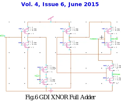
Fig.6 GDI XNOR Full Adder
VI. RESULT AND DISCUSSION
The conventional method for Wallace tree gives maximum delay and power dissipation than the modified method. The Transmission Gate Adder (TGA) gives the lowest delay which is a major requirement in the Wallace tree multiplier, but it consumes more power than the conventional one. Gate Diffusion Input (GDI) does a better trade-off between power, delay and area as shown in the table below
TABLE 1: Full Adders used in Wallace Tree Multiplier
DELAY (ns) No. of TRANSISTOR POWER DISSIPATI ON (mW)
CMOS 136.9 36 3.952
DPL 114.1 36 0.156
TGA 16.6 14 4.72
GDI 88.6 10 2.91
VII.CONCLUSION
Nowadays different types of techniques like Wallace tree is being used for fast multiplication, booth encoder reduces the number of input bits as per the required output. The most important block in Wallace tree multiplier is the adder. So by reducing the delay, area and power of an adder we can improve the overall performance of Wallace tree multiplier. From the above results it is noted that Gate Diffusion Input (GDI) is best trade-off for high speed Wallace tree multiplier. The result is from Tanner EDA 18nm technology.
REFERENCES
[1] Chepurisatish, PanemcharanArur, G.Kishore Kumar and G.Mamatha, “An Efficient High Speed Wallace Tree Multiplier”, International Journal of Emerging Trends in Electrical and Electronics (IJETEE), Vol.10, No.4, p.p.(2320-9569), May. 2014.
[2] N. Prathima and K. Hari Kishore, “Design of a low power and high performance digital multiplier using a novel 8T adder”, International Journal of Engineering Research and Applications (IJERA), Vol.3, No.1, p.p.(1832-1837), January February 2013.
[3] Soniya and Suresh Kumar, “A Review of Different Type of Multipliers and Multiplier Accumulator Unit”, International Journal of Emerging Trends & Technology in Computer Science (IJETTCS), Vol.2, No.4, p.p.(364-368), July – August 2013.
[4] E. Prakash, R. Raju and Dr.R. Varatharanjan, “Effective method for Implementation of Wallace Tree Multiplier using Fast Adders”, Journal of Innovative Research and Solutions (JIRAS), Vol.1, No.1, p.p.(88-94), July-Dec 2013.
[5] Shruti Dixit, Praveen Kumar Pandey, “FPGA Implementation of Wallace Tree Multiplier using CSLA / CLA”, International Journal of Science and Research (IJSR), Vol.2, No.12, p.p.(314-318), December 2013.
[8] Vasudev G. and RajendraHegadi, “Design and Development of 8-Bits Fast Multiplier for Low Power Applications”, IACSIT International Journal of Engineering and Technology, Vol. 4, No. 6, p.p.(774-780), December 2012.
[9] PuneetBhardwajDhammi, “Analysis and Implementation of various Adders and Multipliers with Power and Performance Perspectives”, Thapar University Patiala, July 2011.
[10] Ravi Nirlakalla, ThotaSubbaRao, TalariJayachandra Prasad, “Performance Evaluation of High SpeedCompressors for High Speed Multipliers”,Serbian Journal of Electrical Engineering, Vol.8, No.3, p.p.(293-306), November 2011.
[11] Shiv Shankar Mishra, Adarsh Kumar Agrawal and R.K. Nagaria, “A comparative performance analysis of various CMOS designtechniques for XOR and XNOR circuits”,International Journal on Emerging Technologies, Vol.1, No.1, p.p.(1-10), Feb. 2010.
![Fig.1 Wallace Tree Multiplier[6]](https://thumb-us.123doks.com/thumbv2/123dok_us/7787159.1288721/2.595.197.397.509.669/fig-wallace-tree-multiplier.webp)