ISSN (Print) : 2320 – 3765 ISSN (Online): 2278 – 8875
I
nternational
J
ournal of
A
dvanced
R
esearch in
E
lectrical,
E
lectronics and
I
nstrumentation
E
ngineering
(An ISO 3297: 2007 Certified Organization)
Vol. 5, Issue 11, November 2016
Gate Driven Coupled Bulk Driven
Hybrid Current Mirror
Premanand.B1, Sreeraj V.P2
Assistant Professor, Dept. of ECE, Government Engineering College, Idukki, Kerala, India1
PG Student [VLSI& Embedded Systems], Dept. of ECE, Government Engineering College, Idukki, Kerala, India2
ABSTRACT: A major component in these analog circuits is the current mirror, especially a high impedance current mirror in the case of biomedical applications. The project aims at the design of a cascode current mirror. The general trend followed is the lowering of the supply voltage and scaling down of the device geometry to make the device faster with minimal power consumption. The main obstacle in the supply reduction of circuits is the threshold voltage. Bulk-driven (BD), sub-threshold operation, floating gate (FG) and quasi-FG (QFG) are some of the widely used techniques to overcome the threshold voltage limitation.This paper aims to combine gate driven and bulk driven technologies in a cascode current mirror. The aim has achieved.
KEYWORDS: Current mirror, power consumption,Gate driven, paper,Bulk driven.
I. INTRODUCTION
We use current mirror to get different values of current from a single current source. This can be proved from the drain current equation of MOSFET. NMOS current mirrors have current sinking property while PMOS have current sourcing property.In the early 1980s many experts predicted the demise of analog circuits. Many functions that had been traditionally realized in analog form were now easily performed in the digital domain. But still analog designers are of great demand today. This is because there are many areas where it is very difficult or even impossible to replace analog functions with their digital counterparts regardless of advancements in technology. Digitization often requires analog blocks before digitizing. A major component in these analog circuits is the current mirror, especially a high impedance current mirror in the case of biomedical applications. The project aims at the design of a current mirror. The fundamental design of this circuit is a high-swing super-Wilson, which offers high output impedance using negative feedback. A feedback action is used to force the input and output currents to be equal. The increasing demand for efficient portable electronic equipment has pushed the industry to produce circuit designs with very low power consumption. The general trend followed is the lowering ofthe supply voltage and scaling down of the device geometry to make the device faster with minimal power consumption. The main obstacle in the supply reduction of circuits is the threshold voltage. Bulk-driven (BD), sub-threshold operation, floating gate (FG) and quasi-FG (QFG) are some of the widely used techniques to overcome the threshold voltage limitation. Unfortunately, these techniques suffer low transconductance and hence experience lower bandwidth. This paper aims to combine gate driven and bulk driven technologies in a cascode current mirror. The aim is realized.
II. EXISTING CIRCUITS
A. GATE DRIVEN CURRENT MIRROR
ISSN (Print) : 2320 – 3765 ISSN (Online): 2278 – 8875
I
nternational
J
ournal of
A
dvanced
R
esearch in
E
lectrical,
E
lectronics and
I
nstrumentation
E
ngineering
(An ISO 3297: 2007 Certified Organization)
Vol. 5, Issue 11, November 2016
The auxiliary current sources are replaced by PMOS. M2 and M4 act as a current mirror. To achieve high output impedance M1 is modified as a cascaded one; ie instead of Vgs a transistor is used. M2 and M4 samples Iout, compares it with Iin, and through M5 changes Iout and make it equal to Iin. M6 and M7 are PMOS, they act as active load and improves output impedance. PMOS is used because holes’ mobility is low and thus leakage current reduces.
The disadvantage of this circuit is, overdrive voltage is low. The transistor need VT (Threshold Voltage) to become ON. If we give a Vgs greater than VT, the excess voltage there is known as overdrive voltage. When overdrive voltage increases the conductivity of transistor will increase. Here Vgs=0; why because gate and source of PMOS are shorted. For a PMOS to be in saturation the condition is Vgs – VT≥Vds . This equation becomes –VT ≥ Vds; ie VT ≤ Vds .
Thus overdrive is not present means it is low.
B. MODIFIED GATE DRIVEN CURRENT MIRROR
Fig. 2. Modified Gate Driven current mirror
To overcome the disadvantage of previous circuit, this new circuit comes. Here the short between the gate and source of both PMOS are removed. A bias voltage is given at the gate of both PMOS. Here Vgs ≠ 0. Vgs – VT ≥ Vds is the
condition for saturation. Vgs = Vb1 – Vdd, a voltage higher than Vds is present at the gate terminal. The overdrive voltage is improved.
C. BULK DRIVEN CURRENT MIRROR
The increasing demand for efficient portable electronic equipment has pushed the industry to produce circuit designs with very low power consumption. The general trend followed is the lowering of the supply voltage and scaling down of the device geometry to make the device faster with minimal power consumption.
Fig. 3. Bulk driven current mirror
ISSN (Print) : 2320 – 3765 ISSN (Online): 2278 – 8875
I
nternational
J
ournal of
A
dvanced
R
esearch in
E
lectrical,
E
lectronics and
I
nstrumentation
E
ngineering
(An ISO 3297: 2007 Certified Organization)
Vol. 5, Issue 11, November 2016
D. BULK DRIVEN CASCODE CURRENT MIRROR
Fig. 4. Bulk Driven Cascode Current Mirror
Cascode current mirrors are used, to achieve high output resistance.If we apply signal to the bulk instead of to the gate, and keeping VGS constant then device operate as bulk-driven MOS transistor. Vbs2 = Vds2, and Vbs4 = Vds4. Q2 and
Q4 operates in linear region which forces the Q3 and Q5 to operate in linear region, therefore Iout is forces to match Iref.
CMOS transistor Iref current flows through the Q2Transistor. Iout current try to follow the Iref current.
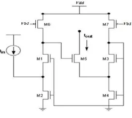
III.PROPOSED CIRCUIT
This paper aims to combine gate driven and bulk driven technologies in a cascode current mirror. Improvement in output impedence is targeted. Reduction in voltage requirement is targeted. Improvement in input current range is targeted. Here the gate driven technology and bulk driven technology are combined in a cascode current mirror. The expectations are improvement in output impedance and input current range. The power consumption has to be reduced.
Fig. 5. Block diagram of Proposed system
Improvement in matching of input and output current is achieved. For 5uA input current 4.90 A output current has got. Improvement in input current range also achieved. The current range of new proposed circuit is 5-50 A. Better than existing circuits. Output impedance has also improved. For proposed circuit it is 367.54K Ohm.
ISSN (Print) : 2320 – 3765 ISSN (Online): 2278 – 8875
I
nternational
J
ournal of
A
dvanced
R
esearch in
E
lectrical,
E
lectronics and
I
nstrumentation
E
ngineering
(An ISO 3297: 2007 Certified Organization)
Vol. 5, Issue 11, November 2016
IV. SIMULATION RESULTS
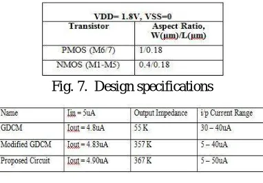
The circuits are simulated using Cadence design environment in of 180nm CMOS technology. The design specifications for Low Voltage High Swing Super Wilson Current Mirror and improved version are mentioned in Table I. The simulation results and dc analysis have been presented to demonstrate the feasibility of proposed current mirror circuit.
Fig. 7. Design specifications
Fig. 8. Comparison of different current mirrors
The Proposed Current Mirror is improved better than other current mirrors. We can understand that fact from the table.
Fig. 10. Proposed Circuit (Output Impedance)
ISSN (Print) : 2320 – 3765 ISSN (Online): 2278 – 8875
I
nternational
J
ournal of
A
dvanced
R
esearch in
E
lectrical,
E
lectronics and
I
nstrumentation
E
ngineering
(An ISO 3297: 2007 Certified Organization)
Vol. 5, Issue 11, November 2016
Fig.10 Layout of Proposed Circuit
V. CONCLUSION
The design of a new very-high output impedance current mirror using output current sampling that has low input and output voltage requirements. The circuits are simulated using Cadence design environment in of 180nm CMOS technology, simulations show that the value of the output current is main-tained within 2% of that of the input current. The proposed circuit offers very high impedance due to the presence of the PMOS at both legs since no auxiliary biasing circuit is used. Various current mirrors are studied. Basic current mirror , Wilson current mirror , Cascode current mirror , Super Wilson current mirror , Super wilson current mirror with low inputvoltage, High Swing Super Wilson Current mirror, Improved High Swing Super Wilson Current Mirror, Low voltage High impedance Current Mirror, Low Voltage High Swing Super Wilson Current Mirror, Gate driven current mirror, Bulk driven current mirror are studied. Each has its own merits and demer-its. The proposed circuit is a combination of Gate Driven and Bulk Driven technologies. The circuit is realized. Improvement in performance are got. The proposed circuit can be modified to produce very high impedance at the weak inversion region for ultra deep sub-micron technology. Since we are not using the auxiliary current source, the negative leakage current can be totally avoided at the weak inversion region, so that the noise interference can be avoided in the implantable chip.
REFERENCES
[1] B. Minch, Low-Voltage Wilson Current Mirrors in CMOS,”in IEEE ISCAS, New Orleans, LA, USA, 2007, pp. 22202223. [2] Trupti .B. Desai, Pratik .P .Shah “Simulation of Bulk Driven Circuits for Low Power Applications” IJETR, Volume-2, Issue-2, 2014.
[3] N.Raj, A.K. Singh and A.K. Gupta “Low –voltage bulk-driven self-biased cascade current mirror with bandwidth enhancement” ELECTRONIC LETTERS, Volume-50, No.1, 2014
[4] Louis-Francois Tanguay, MohamadSawan, and YvonSavaria, A Very-High Output Impedance Current Mirror for Very-Low Voltagen Biomed-ical Analog Circuits,”Circuits and Systems, 2008. APCCAS 2008 IEEE Asia Pacific Conference, 2008, pp. 642-645.
[5] Fabian KHATEB, Nabhan KHATIB, “ New Bulk-driven Class AB CCII”, Dept. of Microelectronics, Brno University of Technology, IEEE, Transaction, 2011.
[6] M.K. Priya, V.K. VanithaRugmoni, A Low Voltage Very High Impedance Current Mirror Circuit and Its Applications,”in IEEE ICCCE, 2013,pp. 511-516.
[7] BhawnaAggarwal, Maneesha Gupta ,“Low-Voltage CascodeCurrent Mirror based on Bulk-Driven MOSFET and FGMOS techniques”, Department of Electronics and Communication Engg., IEEE, Transaction, 2009.
[8 NareshLakkamraju, Ashis Kumar Mal, “A Low Voltage High Output Impedance Bulk Driven Regulated Cascode Current Mirror”, Department of ECE National Institute of Technology, IEEE, Transaction, 2011.
[9] B. Razavi, Design of Analog CMOS Integrated Circuit,” McGraw-Hill.
[10] E. Raghuvaran, A Very High Impedance Current Mirror For Bio- medical Applications, IEEE Transactions on Analog Circuits, 2011, pp 828-830.
[11] BajrangBansal, PrabhatRanjan, HimanshuKaushik Current Mirror Circuits with Improved Performance, IIJEEE, ISSN : 2231 5284, Volume-I, Issue-II, 2011.
[12] P. E. Allen and D. R. Holberg, CMOS analog circuit design, New York: Oxford University Press, 2002.