837 | P a g e
ARITHMETIC LOGIC UNIT DESIGN FOR
REVERSIBLE LOGIC CONDITION USING
REVERSIBLE LOGIC GATES
K.P.Kavipriyan
1,K.Ramya
2,M.Priyavadhana
3, Dr.T.Ravichandran
41234
ECE, SNS COLLEGE OF TECHNOLOGY, (INDIA), [email protected]
ABSTRACT
Using conventional gates like AND& OR gates the digital system is implemented which dissipates a major
amount of energy in the form of bits which gets erased during logical operation.by using reversible logic
circuits in place of conventional logic circuits the problem of energy loss can be solved in digital circuit
designing the reversibility has become the most promising technology. In today’s world ALU is one of the
very important of any system having many applications in computers, cell phones, calculators etc.In this
paper the design of one bit reversible ALU using reversible logic gate is proposed. The proposed ALU is
analysed on FPGA SPARTAN6 device. The proposed design is compared in terms of propagation delay,
quantum cost and garbage outputs. In this paper the 4-bit reversible ALU is also design on proposed 1- bit
reversible ALU architecture.
Keywords: ALU, FPGA SPARTAN6, REVERSIBLE LOGIC, QUANTUM COST, FEYNMAN
GATE.
I.
INTRODUCTION
Growth of computing machines has reached a great success in the past decade.Conventional technologies
such as MOS transistor would reach heights because of exponential growth in transistor density and
especially increasing power dissipation. Various alternatives are required to increase the computational
power of the current generation. Reversible logic gates has become a promising technology withits use in
nanotechnology, quantum computing, low power CMOS and optical computing.The reversible logic was
mainly designed to reduce the quantum cost and garbage outputs. One of the most important problems in
conventional technology is power dissipation. A computing device was designed by landauer in 1961 to
bear the degrees of liberty which will act as a heat sink for the energy required for calculation, resulting in
computing errors.. According to Landauer’s principle, the loss of one bit of information lost, will dissipate
kT*ln (2) joules of energy where, k represents the Boltzmann’s constant and value of k is 1.38x10 -23 J/K,
T is the absolute temperature in Kelvin[12]. The primal combinational logic circuits dissipate heat energy for
eachbit of information that is lost during the operation. This is so because according to second
thermodynamics, once the bit containing information gets lost then it cannot be recovered by any approach or
techniques. The number of bits which was lost during process is directly related to the power dissipate.
838 | P a g e
reduce KTln2 joules of energy dissipation. This technique is possible only if the circuit is reversible logically.
The device which is designed in the field of digital circuits to reduce the power dissipation is called
reversible logic device. The gates which are designed using the logic is called reversible logic gates. Using
instruction set architecture, inputfor execution is determined by the programmer. Based on this arithmetic
logic we should be able to generate variety of logical output. A programmer should receive opcode signals
from fixed input lines of a reversible logic circuit and output result produced from the output lines.
II. ARITHMETIC AND LOGICAL UNIT
An Arithmetic and Logic Unit (ALU) is a digital circuit used to perform arithmetic and logic operation. It is
very important part of a circuit system. It is used in mobile phones, computers, laptops, calculators
etc…Power dissipation occurring because of information loss in ALU can be reduced by reversible logic
gates.
2.1. REVERSIBLE LOGIC GATES
An important step in digital circuit design is design verification and its important thing which acts as
bottleneck in IC development, design verification is of different types, out of which functional verification
takes much effort and time verification. Equivalence checking is important &necessary is check whether the
design is performing all the operations with given curtailment. Equivalence checking has two main classes
they are format based and simulation based equivalence checking.One is equivalence checking done on
simulation based and second is the Equivalence checking done on formal based. Simulation-based
Equivalence Checking is a straight-forward checking but presents many challenges. It needs creation of test
benches for various input states. Also, a There are three basic 2x2 reversible logic gates. The Controlled-Not
gate commonly called the Feynman gate is designed to produce the following output states: P = X and Q = X
xor Y. Since fanout is expressively forbidden in reversible logic, since a fanout has one input and two
outputs, the Feynman gate can be used to duplicate a signal when Y is equal to 0. Quantum cost of Feynman
gate is 1.
Figure 2.1: Block diagram of Feynman Gate
In the reversible logic, a XOR gate can be represented as shown in Fig. 2.2, where A, B and P, Q are the
input and output vectors respectively. Here the mapping between theinputs and outputs can be represented as
P = A and Q = AB .The reconstruction of input vectors from the output vectors can be seen in table 2.1. In
the table 2.1 each output vector corresponds to a unique input vector.
839 | P a g e
R is a 3*3 reversible gate whose block diagram is shown in fig.2.3. Having inputs (X,Y,Z) and outputs
P=Xxor Y; Q= X and R=Z’ xor XY. Quantum cost of R gate is 4.
Figure.2.3. Block Diagram of R Gate
BME is a 4*4 reversible gate whose block diagram is shown in fig.2.4. Having inputs (X,Y,Z,T) and outputs
P=X ’, Q=XY xor Z , R=XT xor Z and S=X’ Y xor Z xor T . Quantum cost of BME gate is 6.
Figure2.4. Block Diagram of BME Gate
The DKG gate is a 4*4 reversible gate whose block diagram is shown in fig.2.5. Having inputs (X,Y,Z,T)
and outputs are P=Y, Q= (X’Z+XT), R= (X xor Y) (Z xor T)(Zxor ZT) and S=(Y xor Z xor T). Quantum
cost of DKG gate is 6. This gate can be used as a half adder as well as a full adder. This gate is designed from
Peres gate.
Figure 2.5: Block Diagram of DKG Gate
In present generation, quantum technology has wide scope in computing system. In addition to reversibility,
it has unique features such as quantum parallelism, quantum entanglement, quantum superposition etc… This
technology helps for solving problems more quickly than electrical computing. (When we calculate in Hilbert
space,quantum circuit is reversible before measurement and after measurement quantum circuit becomes non
reversible because probabilistic measurement cannot be reversed) Only few algorithm are known new
quantum fast Fouriertransform and Grove’s algorithm are few algorithms which is used to solve problems
840 | P a g e
fixed outputs should be considered. Takes an efficient reversible circuit should be designed based on the
analysis. The gates such as BME, FEYNMAN, DKG, MRG, HNG, R are some efficient gates.
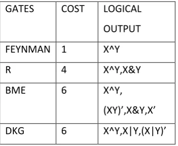
Table 2.2 Cost and Logical outputs of Reversible logic gates
GATES
COST
LOGICAL
OUTPUT
FEYNMAN 1
X^Y
R
4
X^Y,X&Y
BME
6
X^Y,
(XY)’,X&Y,X’
DKG
6
X^Y,X|Y,(X|Y)’
2.2 FAN IN
After the minimization of circuit level and mapping to the primary gates (AND or OR) with infinite fan-in
and fan-out. Minimum circuit Depth is 2 for all logic circuits in accord to this definition. Since any logic
functions can be expressed in sum of product form without any fan-in that limits all the product expressions
can be executed by AND gates and summed by one OR gate. The acute path embraces in one AND gate and
one OR gate, corresponds to circuit depth of 2. The assumption of infinite fan-in and fan-out are invalided.
2.3. FAN OUT
[3]The current from the output is sufficient to charge the load gate(s’) input capacitor(s’) and wire capacitor
within time. For OE circuits the maximum fan-out is limited by the ratio of the gate’s output. After
minimizing the circuit might require large fan-out that is beyond the maximum fan-out limits to the existing
gate. Both methods cause circuits to increase in depth. To evaluate the circuit depth increase caused by
limiting fan-out. A large gate fan-out is significant in succeeding a smaller circuit depth.
III. PROPOSED METHODOLOGY
Parallel adder is the basic part of arithmetic part of ALU. A parallel adder is built with full adders and 1 bit
and 4 bit reversible ALU’s. The reversible ALU uses DKG gates as full adder. Cin enters the fulladder as
carry input in its least important bit position and exists out as Cout . The output of the full adder is taken as
sum. Since we are using arithmetic operation the arithmetic addition is realised when one set of inputs enters
through A inputs and other set enters through B inputs and input carry is kept 0.When Cin =1 it is possible to
add 1 to the sum in Functions, if we complement all the bits of B then we will get F= (A+B). And when
CIN= 1 we will get F= (A-B). Similarly if all inputs of B is 0, we get the transfer A function. The proposed 1
and 4-bit ALUs is shown in figure 2.6. and logical outputs based on inputs opcodes are shown in Table
2.3.(a) and (b).
841 | P a g e
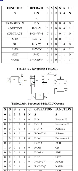
Fig. 2.6 (a). Reversible 1-bit ALUTable 2.3(b). Proposed 4-Bit ALU Opcode FUNCTION S OPERATI ON S S 0 S 1 S 2 S 3 S 4 CI N
TRANSFER X F=X 0 0 0 0 0 0
ADDITION F=X+Y 0 0 0 0 0 1
SUBTRACT F=X+Y’+1 0 0 1 0 1 0
XOR F=X Y 0 0 0 0 1 1
OR F=X^Y 1 0 0 1 0 0
AND F=X&Y 0 0 0 1 0 1
NOT F=X’ 0 0 0 1 1 0
NAND F=(X&Y)’ 0 1 0 1 1 1
S 0 S 1 S 2 S 3 S 4 Cl N OPERATION S FUNCTION S
0 0 0 0 0 0 F=X Transfer X
0 1 0 0 0 0 F=X+1 Increment X
0 0 0 0 0 1 F=X+Y Addition
0 0 1 0 1 0 F=X+Y’+1 Subtract
1 0 0 1 0 0 F=X-1 Decrement X
0 0 0 0 1 1 F=X^Y XOR
1 0 0 1 0 0 F=X|Y OR
0 0 0 1 0 1 F=X&Y AND
0 0 0 0 0 0 F=X’ NOT
0 0 1 1 1 0 F=(X^Y)’ XNOR
0 0 0 1 1 0 F=(X&Y)’ NAND
842 | P a g e
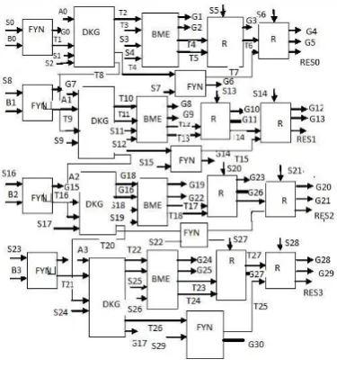
Fig. 2.6 (b). Reversible 4-bit ALUThe proposed 4-Bit ALU is higher in terms of delay, quantum cost than the proposed 1-Bit ALU. The
presented ALUs has two most important advantages. First, it produces less delay than the existing 1-Bit
logic architecture. As a result, the proposed ALU has a better quantum delay for n-bit ALUs. Second,
proposed ALU produces more arithmetic and logical operations. The proposed ALU is designed to be
flexible so that any alterations required for implementation in an instruction set architecture will be easy.
IV. SIMULATION RESULTS
The proposed 1-bit and 4-bit ALU architecture presented and explained in the previous section is synthesized
and simulated on XILINX ISE. The simulation waveforms of both 1 and 4-bit ALUs are shown in
figure.2.7(a) and (b.)
Fig 2.7 (a). Simulation waveform of Reversible 1-bit ALU
Fig. 2.7 (b). Simulation waveform of Reversible 4-bit ALU
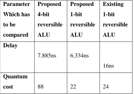
Table 2.4 show the performance comparison of the existing ALU design with the proposed reversible ALU
designs. For comparison, propagation delay, ,quantum cost and garbage output are considered as the
843 | P a g e
Table 2.4 comparison of existing ALU design
V. CONCLUSION
The proposed reversiblegate has been studied using reversible ALU. The design of new ALU is advantageous
for implementation of delays and logical output calculations. The designs which are proposed can be
integrated using n bit ALU. The existing 1 bit ALU has much delay compared to proposed 1 bit ALU. The
garbage and quantum cost is small to design n bit ALU using this proposed method. The circuits must be
garbage free but most of the design implements conventional algorithms with garbage. The ultimate aim is to
reduce logic size or number of garbage bits, using reversible gates this approach may be helpful in gaining
knowledge about fixed size circuits and design
REFERENCES
[1].Robert wille,”Introdution to Reversible Circuit Design”,Electronics Communication and Photonics
Conferences (SIECPC), 2011 Saudi International, E-ISBN:
978-1-4577-0067-5,Print-ISBN:978-1-4577-0068-2,IEEE,2011.
[2].Nagamani, A.N.; Ashwin, S.; Agrawal, V.K., "Design of optimized reversible Binary and BCD adders,"
VLSI Systems, Architecture, Technology and Applications (VLSI-SATA), 2015 International Conference
on , vol., no., pp.1,5, 8-10 Jan. 2015.
[3].Balaji G.Naveen, Pandian S. Chenthur, Rajesh D., “Fast Test Pattern Generator using ATALANTA M
2.0” Asian Journal of Research in Social Sciences and Humanities, ISSN : 2249-7315, Vol.7, Issue:2 ,
pp.721-729, Feb 2017.
[4].Khurana, S.; Grover, A.; Grover, N., "Comparative Analysis: Power Reversible Comparator Circuits 90
NmTechnology," Modelling Symposium (AMS), 2013 7th Asia, vol.,no., pp.103,107, 23-25 July 2013.
[5].Banerjee, A.; Das, D.K., "Squaring in reversible logic using iterative structure," Design & Test
Symposium (EWDTS), 2014 East-West, vol., no., pp.1,4, 26-29 Sept. 2014.
[6].Jagannatha, K.B.; Divya, D.; Reddy, K.S.; Desai, P.K.; Sevanthi,S., "ASIC design of reversible full adder
circuits," Computing, Electronics and Electrical Technologies (ICCEET), 2012 International Conference
on , vol., no., pp.734,737, 21-22 March2012.
Parameter Which has to be compared Proposed 4-bit reversible ALU Proposed 1-bit reversible ALU Existing 1-bit reversible ALU Delay
7.885ns 6.334ns
16ns
Quantum
844 | P a g e
[7].Nagamani, A.N.; Ashwin, S.; Agrawal, V.K., "Design of optimized reversible binary adder/subtractor and
BCD adder," Contemporary Computing and Informatics (IC3I), 2014 International Conference on , vol.,
no., pp.774,779, 27-29 Nov. 2014.
[8].MdHasanBabu, H.; Saleheen, N.; Jamal, L.; Sarwar, S.M.; Sasao,T., "Approach to design a compact
reversible low power binary comparator," Computers & Digital Techniques, IET , vol.8, no.3,pp.129,139,
May 2014.
[9]. P.R.Yelekar and Prof. Sujata S Chiwande. Article: Introduction toreversible logic Gates & its
Application. IJCA Proceedings on 2ndNational Conference on Information and Communication
TechnologyNCICT(8):5-9, November 2011.268.
[10].HimanshuThapliyal and A.p.Vinod, Desining Efficient Online Testable Reversible Adder with New
Reversible Adder with New Reversible Gate .IEEE-2007,1085-1088.
[11].L.M.K.VandersypenM.SteffenG.Breyta C.S. YannoniM.H.Sherwood. I.L.Chuang “Experimental
realization of Shor’s quantum factoring using nuclear magnetic resonance
“<em>Nature</em>vol.414pp.8832001.
[12].A Dixit and V.Kapse , “Arithmetic & Logic Unit (ALU) Design using Reversible Control Unit”
,International Journal of Engineering and Innovative Technology, vol. 1,pp. 55-60,2012.
[13].Morrison, M.; Ranganathan, N., "Design of a Reversible ALUBased on Novel Programmable
Reversible Logic GateStructures," VLSI (ISVLSI), 2011 IEEE Computer Society AnnualSymposium on ,
vol., no., pp.126,131, 4-6 July 2013.
[14].Sharma, S.; Singh, S.B.; Akashe, S., "Optimized powerperformance and simulation of reversible
logicmultiplexer," Emerging Research Areas and 2013 International Conference on Microelectronics,
Communications and RenewableEnergy(AICERA/ICMICR), 2013 Annual InternationalConference on ,
vol., no., pp.1,6, 4-6 June 2013.
[15].Roohi, A.; Khademolhosseini, H.; Sayedsalehi, S.; Navi, K.,"Implementation of reversible logic design
in nanoelectronics onbasis of majority gates," Computer Architecture and DigitalSystems (CADS), 2012
16th CSI International Symposium on ,vol., no., pp.1,6, 2-3 May 2012.
[16].Sayem, A.S.M.; Mitra, S.K., "Efficient approach to design lowpower reversible logic blocks for Field
Programmable GateArrays," Computer Science and Automation Engineering (CSAE),2011 IEEE
International Conference on , vol.4, no., pp.251,255,10-12 June 2011.
[17].Kaur P., Dhaliwal B.S., "Design of fault tolerant full Adder/Subtarctor using reversible gates,"
ComputerCommunication and Informatics (ICCCI), 2012 InternationalConference on , vol., no., pp.1,5,
10-12 Jan. 2012.
[18].Banerjee, A., "Reversible cryptographic hardware with optimizedquantum cost and delay," India
Conference (INDICON), 2010Annual IEEE , vol., no., pp.1,4, 17-19 Dec. 2010.
[19].Grover, A., "Design of Power Reversible Comparators withDifferent Technologies," Computational
Intelligence, Modellingand Simulation (CIMSim), 2013 Fifth International Conferenceon , vol., no.,
pp.193,196, 24-25 Sept. 2013.
[20].P. Gupta, A. Agrawal, and N. K. Jha, “An algorithm for synthesis of reversible logic circuits,” IEEE
845 | P a g e
[21].W.D. Pan; M.Nalasani,”Reversible logic “, Volume: 24,Issue: 1,IEEE Journals & Magazines Year:
2005 DOI: 10.1109/MP.2005.1405801, IEEE 200
[22].A.Khazamipour, A.KatarzynaRadecka. A New Architecture of Adiabatic Reversible Logic Gates,