MARKS, JEFFERY EARL. SOI for Frequency Synthesis in RF Integrated Circuits. (Under the direction of Dr. Wentai Liu.)
SOI for Frequency Synthesis in RF Integrated Circuits
by
Jeffery Marks
A thesis submitted to the Graduate Faculty of
North Carolina State University
in partial fulfillment of the
requirements for the Degree of
Master of Science
Department of Electrical and Computer Engineering
Raleigh
2003
Approved By
Biography
Jeff Marks was born on May 25th 1976 in Port Huron, Michigan. He received his undergraduate degree in Computer Engineering from North Carolina State University in
December of 1999. At various times during his academic career, Jeff financed his education by working as an Office Depot merchandise stocker, a bicycle mechanic, courier, computer help desk attendant, an employee of the Intel Corporation and Alcatel Network Systems, a circuits lab teaching assistant, a digital electronics teaching assistant
Acknowledgements
Most importantly I would like to acknowledge the input and mentoring provided by Dr. Kasin Vichienchom, who patiently provided the guidance that made this work possible. Kasin’s knowledge combined with his dedication, patience and humility have set in my mind, and incredibly high standard of what is expected of a scholar.
I also have to give my thanks to the other denizens of the fourth floor of EGRC. Kasin, Rajeev, Ramya, Rizwan and Mustafa have all been my technical advisors, social network, support group and most importantly my friends. These co-workers made spending the insanely long hours in room 429 fun. I don’t think I could have asked for a better work environment.
Table of Contents
List of Figures... vi
List of Tables... ix
Chapter 1 Introduction... 1
1.1 Introduction and Motivation ... 1
1.2 Scope... 2
1.3 Organization... 3
Chapter 2 Literature Review... 4
2.1 Developments In Frequency Synthesis... 4
2.2 PLL Basics ... 5
2.2.1 Integer N PLL ... 5
2.2.2 Fractional N Frequency Synthesis ... 6
2.3 Current Developments In Frequency Synthesis for RF Applications... 11
2.3.1 Developments in VCOs ... 11
Chapter 3 Development of an integrated frequency synthesizer in SOI. ... 18
3.1 Building Blocks of the PLL ... 18
3.1.1 Component: Phase Frequency Detector and Charge Pump ... 19
3.1.2 Component: Loop filter... 24
3.1.3 Component: VCO ... 25
3.1.4 Component: Divide By N ... 27
3.2 System Analysis... 28
3.3 System Design ... 30
3.3.1 Determining Design Variables... 31
3.3.2 Solving the System Equations ... 32
3.3.3 Design Results ... 34
3.4 Fabrication of the PLL ... 41
3.4.1 Testing of the PLL ... 42
3.4.2 PLL Testing Results... 46
3.5 Conclusions... 49
Chapter 4 Characterization of the Honeywell SOI devices and circuits ... 51
4.1 Individual Device Characterization ... 51
4.2 Design and Layout ... 52
4.2.1 Individual Device Testing... 54
4.2.2 Individual Device Results ... 55
4.3 Individual Device Conclusions ... 59
4.4 Oscillator Characterization ... 59
4.4.1 Oscillator Design Overview... 60
4.4.2 Oscillator Simulation and Layout ... 61
4.4.3 Oscillator Testing... 65
4.4.4 Oscillator Frequency Results ... 66
4.4.5 Implications of the Frequency Results... 69
4.5 Oscillator Timing Jitter ... 70
4.5.1 Oscillator Timing Jitter Testing... 70
4.5.2 Oscillator Timing Jitter Results ... 72
Chapter 5 Jitter Reduction in SOI Ring Oscillators ... 79
5.1 Introduction... 79
5.2 Experiment... 80
5.3 Results... 81
5.4 Conclusions... 82
Chapter 6 Conclusion ... 83
Appendix A Introduction to SOI ... 84
A.1 Devices studied in this work... 86
A.2 Modeling of SOI device operation... 89
A.2.1 Parasitic Currents of the SOI device... 90
A.2.2 Junction Diodes and Parasitic Capacitance... 92
A.3 SOI Noise and Nuances ... 93
Appendix B Individual Device Characterization Data... 96
Appendix C Oscillator Measurements ... 142
List of Figures
Figure 1.1 Frequency Synthesis Applications ... 2
Figure 2.1 Fundamental Frequency Synthesizer Architecture... 5
Figure 2.2 Demonstration of Pulse Removal... 6
Figure 2.3 Architecture Of A Dual Modulus Synthesizer ... 7
Figure 2.4 Dual Modulus Architecture ... 7
Figure 2.5 Fractional N Frequency Synthesis Operation... 8
Figure 2.6 Showing the need to reduce spurs ... 9
Figure 2.7 Noise Shaping... 9
Figure 2.8 SD modulator architecture... 10
Figure 2.9 Tally of JSSC Results... 11
Figure 2.10 Ring Inverter... 12
Figure 2.11 Examples of Delay Stages ... 12
Figure 2.12 Negative Resistance Concept ... 14
Figure 2.13 Negative gm Oscillators ... 15
Figure 2.14 Negative gm Oscillator Using Differential Amplifiers ... 16
Figure 3.1 Block Diagram of the PLL ... 18
Figure 3.2 System Representation of PLL... 19
Figure 3.3 Block Diagram of the Charge Pump and Phase Detector... 20
Figure 3.4 Charge Pump ... 20
Figure 3.5 Phase Detector Gain ... 21
Figure 3.6 Charge Pump Circuit ... 22
Figure 3.7 Phase Frequency Detector ... 23
Figure 3.8 Operation of PFD and Charge Pump... 23
Figure 3.9 Loop Filter Circuit and Block Diagram... 24
Figure 3.10 Operation of Charge Pump and Loop Filter ... 25
Figure 3.11 Block Diagram of the VCO... 25
Figure 3.12 Current Starved Voltage Controlled Oscillator ... 26
Figure 3.13 Layout of the VCO ... 27
Figure 3.14 Divide By N Circuit... 28
Figure 3.15 Phase and Magnitude Response of the PLL ... 29
Figure 3.16 Effect of Ripple Capacitor on Phase and Gain... 30
Figure 3.17 Process Design Flow ... 34
Figure 3.18 Plot of the Phase Response of the Simulated PLL ... 35
Figure 3.19 Gain of the Simulated PLL... 35
Figure 3.20 Effect of External Loop Filter Adjustment on the PLL... 37
Figure 3.21 Circuit Simulation of the PLL Achieving a Lock ... 38
Figure 3.22 Layout of the PLL on the Chip... 39
Figure 3.23 Picture of the Fabricated PLL... 41
Figure 3.24 Placement of the SOI die in the Package... 42
Figure 3.25 Noise on the Power Rail of the Output Buffer ... 43
Figure 3.26 Output Signal of the Buffer ... 44
Figure 3.27 Capacitive Coupled Buffer Noise to other Nodes of the Circuit... 45
Figure 3.28 Plots of KVCO Based on Measurements and Simulations ... 47
Figure 4.1 Layout of Devices... 52
Figure 4.2 Arrangement of Devices on the Die ... 53
Figure 4.3 Peripheral Location of Individual Devices... 54
Figure 4.4 Test Fixture... 55
Figure 4.5 Process Corners of the Fabricated Devices ... 57
Figure 4.6 Effect of Body Bias on Threshold Voltage ... 58
Figure 4.7 Structure of the Fabricated Ring Oscillators ... 59
Figure 4.8 Method for Achieving Equal Rise and Fall Time ... 62
Figure 4.9 Equal Loading of Each Stage ... 62
Figure 4.10 Layout of Ring Oscillators ... 63
Figure 4.11 Equal Interconnect Between Each Stage... 64
Figure 4.12 Accuracy of Simulations Compared to Measurements ... 68
Figure 4.13 Use of Measurements in Achieving Accuracy in Future Fabrications... 70
Figure 4.14 Two Jitter Measurements From the Same Oscillator ... 72
Figure 4.15 Layout of Low-Noise and Normal Inverter Stages ... 77
Figure 5.1 Body Biased Oscillator Layout ... 80
Figure A.1 Processing steps in Soitec Unibond process [] ... 84
Figure A.2 Side view of a fully depleted SOI device ... 85
Figure A.3 Cross Section of a partially depleted SOI device ... 85
Figure A.4 An independently body biased NMOS device ... 86
Figure A.5 A Source to Body Tied NMOS device ... 87
Figure A.6 Transistor stack exploiting SB-tied NMOS devices... 88
Figure A.7 A floating body transistor ... 89
Figure A.8 Circuit representation of SOI device ... 90
Figure A.9 Magnitude of electric field as a function of channel length. ... 91
Figure A.10 Path of Body Discharge in Source Tied and Floating Body Devices... 94
Figure A.11 Demonstration of Data Dependent Behavior of SOI... 95
Figure B.1 PMOS BT, l = 600n, w = 27.75u... 97
Figure B.2 PMOS, l = 600n, w = 13.75u, 14u ... 98
Figure B.3 PMOS, l = 600n, w = 13.75u, 14u ... 99
Figure B.4 PMOS, l = 900n, w = 18u ... 100
Figure B.5 PMOS, l = 900n, w = 18u ... 101
Figure B.6 PMOS, l = 900n, w = 27u ... 102
Figure B.7 PMOS, l = 900n, w = 27u ... 103
Figure B.8 PMOS, l = 900n, w = 18.5u ... 104
Figure B.9 PMOS, l = 900n, w = 18.5u ... 105
Figure B.10 PMOS, l = 900n, w = 18.5u ... 106
Figure B.11 PMOS, l = 900n, w = 18.5u ... 107
Figure B.12 PMOS, l = 600n, w = 13.5u, 13.5u ... 108
Figure B.13 PMOS, l = 600n, w = 13.5u, 13.5u ... 109
Figure B.14 PMOS, l = 950n, w = 19u x 4 ... 110
Figure B.15 PMOS, l = 950n, w = 19u x4 ... 111
Figure B.16 NMOS, l = 600n, w = 9.25u ... 112
Figure B.17 NMOS, l = 600n, w = 9.25u ... 113
Figure B.18 NMOS, l = 600n, w = 9.25u ... 114
Figure B.20 NMOS, l = 600n, w = 4.85u, 4.4u ... 116
Figure B.21 NMOS, l = 600n, w = 4.85u, 4.4u ... 117
Figure B.22 NMOS BT, l = 900n, w=6u ... 118
Figure B.23 NMOS, l = 900n, w = 6u ... 119
Figure B.24 NMOS, l = 900n, w = 6u ... 120
Figure B.25 NMOS, l = 900u, w = 6u ... 121
Figure B.26 NMOS, l = 900n, w = 6u ... 122
Figure B.27 NMOS, l = 900n, w = 6u ... 123
Figure B.28 NMOS, l = 600n, w = 4.4u ... 124
Figure B.29 NMOS, l = 600n, w = 4.4u ... 125
Figure B.30 NMOS, l = 600n, w = 4.4u ... 126
Figure B.31 NMOS, l = 600n, w = 9.25u ... 127
Figure B.32 NMOS, l = 600n, w = 9.25u ... 128
Figure B.33 NMOS, l = 600n, w = 9.25u ... 129
Figure B.34 PMOS, l = 500n, w = 18.5u ... 130
Figure B.35 PMOS, l = 500n, w = 18.5u ... 131
Figure B.36 PMOS, l = 900n, w - 18u... 132
Figure B.37 PMOS, l = 900n, w = 18u ... 133
Figure B.38 NMOS, l = 600n, w = 9.25u ... 135
Figure B.39 NMOS, l = 600n, w = 9.25u ... 136
Figure B.40 NMOS, l = 600n, w = 9.25u ... 137
Figure B.41 NMOS, l = 500n, w = 6u ... 138
Figure B.42 NMOS, l = 500n, w = 6u ... 139
Figure B.43 NMOS, l = 950n, w = 6u ... 140
List of Tables
Table 3.1 Fixed Design Variables for the PLL ... 32
Table 3.2 Performance Requirements for the System ... 33
Table 3.3 Final Values Chosen for Circuit Implementation ... 34
Table 3.4 Performance of Simulated PLL ... 34
Table 3.5 Pin Assignments for the PLL... 40
Table 3.6 Signal Jitter Compared to VCO Control Voltage ... 48
Table 4.1 Performance of Body Biased Devices ... 56
Table 4.2 Performance of Source Tied to Body Devices... 56
Table 4.3 List of Oscillators Fabricated... 65
Table 4.4 Frequencies of Fabricated Oscillators... 66
Table 4.5 Jitter Measurements of the Ring Oscillators... 73
Table 4.6 Jitter Results by Oscillator Group... 74
Table 5.1 Results of the Body Bias Testing... 81
Chapter 1 Introduction
1.1 Introduction and Motivation
The silicon on insulator (SOI) fabrication process is quickly becoming the answer to the technical challenges facing the integrated circuit (IC) industry. Consumer demands for more integration and high speed operation create a set of problems that SOI technology is uniquely qualified to solve. As the name implies "Silicon on Insulator" refers to the fact that the active MOSFETs are fabricated on an electrically insulating substrate. Some of the advantages (which will be examined in more detail later) include a reduction of substrate noise (allowing higher integration) and a reduction of parasitic capacitance (allowing high operating speed). Producers of high performance digital products (IBM and Intel) have invested in the development of SOI processes to be used in future products. SOI also stands to benefit the aerospace and military as well, for the benefits listed above and the availability of radiation hardening from some of the SOI fabrication facilities.
1.2 Scope
Specifically, this work explores the use of SOI for the frequency synthesis portion of the receiver. This includes a voltage controlled oscillator (VCO) and a means of synthesizing a high frequency signal through frequency multiplication of a low frequency input signal. The direction taken by me and the others working on this receiver, is to explore both a digital and analog architectures for the receiver. Each of these architectures has its own advantages and disadvantages (not to be discussed in this document) and each has distinct requirements for the frequency synthesizer. Figure 1.1 shows a block diagram of the architecture and the required frequency synthesis for each.
Analog Digital
Mixer
437 Mhz LC Oscillator
LNA S/H
172 Mhz Clock
LNA
Figure 1.1 Frequency Synthesis Applications
At the time the designs fabricated for this work the Honeywell MOI5 process was still an experimental process. The device models and circuit libraries were updated on nearly a weekly basis. There was a distinct lack of support from the foundry with respect to the device models there were no published results of the testing of circuits that had been fabricated in the MOI5 process. This environment had a great influence on the circuits and designs that were chosen for the fist and second fabrications. Instead of pursuing complex designs that would be applicable for the end product, the approach taken in this work was to fabricate circuits that involved the least amount of risk. Most of the circuits are fairly simple in design, and have a minimal amount of supporting circuitry (biasing, buffering etc). The goal of this work was to try to learn as much as possible about Honeywell SOI to lay the groundwork for future circuit designs
1.3 Organization
Chapter 2
Literature Review
2.1 Developments In Frequency Synthesis
A search for literature specifically dealing with developments in the area of RF receiver design in SOI, will produce few results. The emergence of SOI into the areas of computing and digital circuit design is still in the beginning stages. While several articles have been published regarding SOI design techniques, or the design of circuit building blocks, there has been only one paper published regarding the development of an RF receiver in SOI [1].Instead of limiting the literature search to the developments in SOI, it makes more sense to review the state of the art in general frequency synthesis for RF applications.
Research in the area of frequency synthesis techniques has developed rapidly over the past ten years. Asynchronous communication, for both board-level and RF systems require a stable clock and/or local oscillator in order to recover the transmitted data. Traditional radios used a resonating crystal to produce such an oscillating signal, but the high-frequency, low-power and small-area requirements of today’s applications require a different approach. Frequency synthesis techniques have been investigated for over 40 years [2]. A now popular topic of research in both industry and academia, the recent interest is generated by the capabilities of modern fabrication processes and the desire to integrate communication systems onto a single chip.
phased locked loop shown in Figure 2.1 below. The system uses a feedback system to turn the low frequency input signal into a high frequency output signal.
2.2 PLL Basics
The input to the system (called the reference frequency) is generated off chip, usually by a resonating crystal that also provides the base frequency of the entire system. In modern consumer and outer-space applications this frequency is usually less than 1 MHz [3]. The output of the system is an oscillating signal produced by an oscillator controlled either by current (ICO) or by voltage (VCO). The output signal φOut is divided by a factor ‘N’ to become φIn where it is compared to the reference φRef .
Compare ControlledOscillator
Transform Error into Voltage
Divide by N Reference
Oscillator
REF
φ φError
Out
φ
In
φ
Cont V
Figure 2.1 Fundamental Frequency Synthesizer Architecture
The comparator generates a signal that reflects the phase error between φIn and φRef . This phase error is then converted into a control voltage or current which is used to tune the VCO (or ICO). When fIn and fRef are equal, the output frequency can be expressed as fOut = N∗ fREF.
2.2.1 Integer N PLL
has other uses in the system and the frequency must be chosen to meet other specifications. Integer N PLLs are limited in their application to systems that require the recovery of data at multiple frequencies or channels. For the Integer N PLL to be effective the channel spacing must be an integer multiple of fRef . This again places strict requirements on the reference oscillator that might not be practical for the system as a whole.
2.2.2 Fractional N Frequency Synthesis
A solution was proposed [4] to allow the use of a ‘fractional’ N to be used in the feedback loop. A fractional N allows greater flexibility in the selection of the output frequency and an ability to receive data on channels with closer frequency spacing. A method of achieving this is based on the “pulse swallower” concept [5]. Figure 2.2 below demonstrates the procedure. An input signal with frequency fIN input to a pulse remover that removes one pulse over a period Td. The output contains a total of
1
−
IN f
Td pulses over a period of Td.
Input to the Pulse Swallower Output of the Pulse
Swallower
Td
t
Figure 2.2 Demonstration of Pulse Removal
The resulting output has a frequency which can be represented as
Td f
fOUT = IN − 1 . By altering the period Td, fOUT can be adjusted to meet the needs of a multi-channel system.
PFD LPF VCO
REF f
OUT f
N N+1
÷
Figure 2.3 Architecture Of A Dual Modulus Synthesizer
If the prescaler divides by N for A output pulses (of the VCO) and by N + 1 for B output pulses, then the equivalent divide ratio is equal to (A+B)/[A/N + B/(N+1)]. This value can vary between N and N + 1 in fine steps by proper choice of A and B. The resulting modulus is sometimes written as N.f, where N and f represent the integer and fractional parts of the modulus. An example of this process can be seen in Figure 2.4 below. If
MHz
fRef =1 and N = 5. Let us assume the presale divides by 5 for 4 reference cycles and divides by 6 for one reference cycle.. The total number of output pulses is therefore equal to 5 x 4 + 6 = 26, whereas the reference produces 5 pulses. In other words, the divide ratio is equal to 5.2 making fRef = 5.2MHz.
PFD LPF VCO
REF f
OUT f
5 6
÷
5
÷
Modulus Control
Figure 2.4 Dual Modulus Architecture
Unfortunately this characteristic has an undesired effect of adding noise to the output spectrum.
VCO Output Divider Output Reference
PD Output
1152 ns
1000 ns 960 ns
Figure 2.5 Fractional N Frequency Synthesis Operation
Filtering the Fractional Spurs
Fractional spurs are caused by the periodic accumulation of phase error in the system. It is easiest to visualize this concept when the VCO was biased at a constant voltage and disconnected from the LPF. The output frequency for this analysis is fOUT = 5.2MHz. In Figure 2.5 each of the first 6 cycles of the divided signal is slightly shorter than the reference period. This causes the phase difference between the reference and the feedback signal grows in every period of fRef , until it returns to zero when divide-by-11 occurs. This has the effect of creating a ramp waveform at the output of the LPF.
f REF f f
f REF
Randomizer
(
N +1)
/N÷
To PD From VCO
Figure 2.6 Showing the need to reduce spurs
Randomization of the modulus in a way that produces an average division factor
(
N+α)
is one approach to solving this problem. This technique in effect converts the systematic factional sidebands to random noise. The idea can be taken one step further by shaping the resulting noise spectrum such that most of its energy appears at large frequency offsets. Thus the noise in the vicinity of the divided carrier is sufficiently small and the noise at higher offset is suppressed by the low-pass filter after the feedback signal is translated to DC by the phase detector.From VCO
Randomizer and Noise Shaping
(
N+1)
/N÷
To PD
f f REF f
f REF
Figure 2.7 Noise Shaping
The noise shaping function required in the above scheme can be realized by use of a
∆ −
Σ modulator. Depicted in Figure 2.7 the modulator generates a binary stream (in the case of dual modulus divider) representing an average value accompanied by
From VCO
(
N+1)
/N÷
To PD
( )
txF fOUT
( )
t bΣ∆
Modulator
Figure 2.8 SD modulator architecture
2.3 Current Developments In Frequency Synthesis for RF
Applications
Nearly all of the recent frequency synthesizers developed for wireless applications rely on one of the techniques described in the section above. Over the past two years 14 articles have appeared in the Journal of Solid State Circuits that focus on the application of a frequency synthesis system to an RF front end design. Figure 2.9 below shows a tally of the frequency synthesis methods used in these applications. These papers usually demonstrate the ability of a frequency synthesizer to be implemented with some new encoding scheme (GFSK, GMSK) or some RF communication standard (DCS, CDMA) [31-35]. Other papers explore the abilities of advanced processes in creating improved circuits.
6
1
Integer N Fractional N
Σ∆ Digital
Figure 2.9 Tally of JSSC Results
2.3.1 Developments in VCOs
voltage controlled oscillators. Research in this area can be more intuitively identified as either analog or digital.
Digital
Digital oscillators are usually based in some form inverter chain as seen in Figure 2.10.
Figure 2.10 Ring Inverter
A simple example of the construction of such an oscillator employs the single stage inverter delay cell as seen in Figure 2.11.a. In order to oscillate, a total phase shift of 360 degrees around the loop at a frequency where the small-signal loop gain is above 0db. In an N-stage ring, each stage contributes a (negative) phase shift of 180/N for a total of 180 degrees.
In -In +
Out + Out
-A A
B
B
A A
(a) (b) (c)
Figure 2.11 Examples of Delay Stages
by swapping two feedback lines in a differential architecture an using an even number of inverting stages. Figure 2.11.b shows the differential version of the ring oscillator introduced explained in previous literature [8,9]. The differential or ECL design shown in Figure 2.11.b offers lower susceptibility to supply noise and easy access to outputs with quadrature phase (for RF communication). The largest disadvantage of this approach is that output amplitude is not full-swing and is dependent on the operating frequency (or bias levels). As the P and N devices are biased to starve the inverter of current, the amplitude of the output waveform will decrease. In digital implementations, additional circuitry is needed to bring the outputs to full-swing, increasing the complexity and power consumption of the circuit. Additionally, as power supply voltages are reduced, the stack-up of the devices poses a problem in the ability to bias the devices into the correct operating region. Figure 2.11.c shows the next step in the evolution of the inversion stage design [10][11]. By cross coupling the PMOS load devices, much like in a differential amplifier, the output voltage swing of the circuit is increased. This design scales easier with process advancement and avoids the complex buffer designs required for the "ECL-like" designs. Nearly all modern frequency synthesis applications use some form of the differential delay stage in the VCO. The superior rejection of noise, and the accessibility to the quadrature outputs makes it more suited to the most common applications [12] [13]. The choice of full-swing or partial-swing must be made with the end application in mind. Partial swing designs are easier to test in high-frequency designs, as a full-swing circuit requires a larger buffer to drive the probe/bonding pad. No one design is superior to the other, and the application and test environment should help to determine the best approach.
Analog
applications (1.8 GHz and above) it is necessary to take an analog approach to the design of the oscillator.
Traditional analog approaches rely on the concept of a 'negative resistance' in order to meet Barkhausen's criteria that the loop gain of a feedback system is unity and that the total phase shift around the loop must be equal to zero (or 180 if the dc feedback is negative). The traditional system used to produce these criteria relies on the properties of an LC tank. Figure 2.12 below shows how producing a 'negative' resistance to cancel the parasitic resistance that co-exists with any passive component. By creating a resistance that is equal and opposite to the parasitic resistance a nearly ideal LC tank circuit can be
created that oscillates at ω =
( )
LC −1.Iin Cp Lp Rp
Iin Cp Lp Rp -Rp Iin Cp Lp
=
LC Tank With Parallel Resistor
LC Tank With Parallel Resistance Cancelled
Figure 2.12 Negative Resistance Concept
Figure 2.13 below shows two implementations of this negative resistance concept. Figure 2.13.a is a single ended configuration while Figure 2.13.b is a cross-coupled dual output configuration. In each case, the transistors are sized so that the resistance seen by the LC tank and the associated parasitic resistance (Rp) is -1/gm. This circuit can be viewed as either a feedback system or a negative resistance in parallel with a lossy tank as long as
the condition:
gm
Vb Vout
(a)
Cp Rp
Lp
Out + Out
-(b)
Cp/2
2Lp
2Rp
-2/gm
Figure 2.13 Negative gm Oscillators
This approach by far is the most common and straight-forward of the different methods of creating an oscillator. Recent research into VCO design has focused on integrating this fundamental design into new technologies and altering the architecture slightly to meet specific application criteria [14-15]. Other recent works have focused on understanding the effects of the individual circuit components on the phase noise of the oscillator and methods of eliminating this noise [16-17]. Such research is important in the development of VCO's for system implementation, however such considerations were not necessary for this initial work.
(a)
R
C1 C2
gm
-gm R
C1 C2
(b)
Figure 2.14 Negative gm Oscillator Using Differential Amplifiers
Figure 2.14 above shows the implementation of the cross coupled differential amplifier used as an oscillator. Figure 2.14.a shows a simplified version of the oscillator, while Figure 2.14.b shows the a more accurate representation of the actual circuit. The active load seen at the output of each of the amplifier stages in Figure 2.14.b is inductive and inserts a pole into the transfer function. This pole is necessary to create a unity gain at finite frequencies that allow the circuit to oscillate.
Chapter 3
Development of an integrated frequency synthesizer
in SOI.
As stated in the introduction, the end goal of the NASA SOI project is a fully integrated radio receiver, which includes the frequency synthesizer. The frequency synthesizer is by necessity one of the most area-hungry blocks of a receiver design. The integrated passive components, the VCO and the divide-by-N circuitry consume a large amount of die space. In the first SOI fabrication, the available die space was divided among three students, and as a result there was room for only one attempt at a frequency synthesizer.
The frequency synthesizer chosen for the first SOI fabrication was an integer N PLL that is to supplement the all-digital receiver architecture. A block diagram of the PLL is shown in Figure 3.1 below.
PFD CHP VCO
5.375 Mhz
Loop Filter
Divide by 32
Output = 172 Mhz
Figure 3.1 Block Diagram of the PLL
3.1 Building Blocks of the PLL
the Jet Propulsion Laboratory [22]. 2) A 5 MHz signal is easy to obtain with the available signal generators. An integer-N architecture was chosen simply because of its relative simplicity compared to any of the fractional N architectures. The integer N design presented the least risk.
Each of the individual blocks of the PLL are best represented in the frequency domain so that the behavior of the system as a whole can be designed intelligently and simulated. The system as a whole can be represented as a feed-back system. Figure 3.2 below shows the block diagram.
−
+
In G(s) Out
N
÷
Figure 3.2 System Representation of PLL
The simple transfer function is
N s G
s G In
Out s
H
) ( 1
) ( )
(
+ = =
Each of the individual blocks of the design must be represented in the final equation.
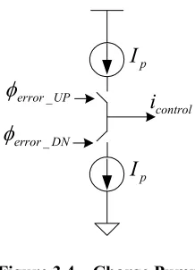
3.1.1 Component: Phase Frequency Detector and Charge Pump
Charge Pump f Re φ In φ control i f / φ Detector UP error_ φ DN error_ φ
Figure 3.3 Block Diagram of the Charge Pump and Phase Detector
Two signals enter the phase/frequency detector one generated by the off-chip reference crystal φRef and one generated by the divide-by-N block φIn. The phase detector detects the phase difference between the two signals and generates two output signals φerror_UP and φerror_DN. These signals indicate whether the phase of the clock should be advanced or delayed in order to be synchronized with the reference signal [23]. The relationship in general can be expressed as:
In f error =Φ −Φ
Φ Re .
This error or 'phase difference' signal is then input to the charge pump circuit.
The charge pump circuit can be visualized as two current switches (Figure 3.4) controlled by the phase-error input signals.
control i UP error_ φ DN error_ φ p I p I
Figure 3.4 Charge Pump
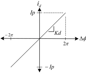
f Re
φ and φIna quantity that was expressed above as φerror. A relationship can be established between the phase error and the output current per cycle
π τ φ 2 ) )( ( p error d
I i =
or the current per period
π φ 2
) )( ( p error d
I
i = .
d
i is the average current per period, it would also be the average current over many periods, or over time t. The relation between output current and phase error then becomes
Kd I s s i p error
d = =
π φ 2 ) ( ) ( ) (
Where Kd is known as the gain of the phase detector, and can be graphically interpreted as the slope of the relation between the average current idand the phase difference ∆φ
(Figure 3.5). d i π 2 − π 2 ∆φ Ip
Ip
−
Kd
Figure 3.5 Phase Detector Gain
3.1.1.1
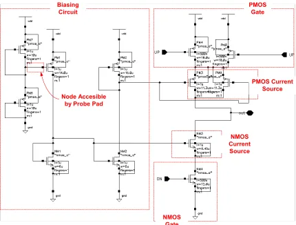
Implementation of the CP and PD
Figure 3.6 and Figure 3.7 show the circuit representation of the phase detector and charge pump respectively.
Biasing Circuit
PMOS Gate
NMOS Gate
NMOS Current Source
PMOS Current Source Node Accesible
by Probe Pad
U p
D o w n R e f e r e n c e
C lo c k
I n p u t S ig n a l
Figure 3.7 Phase Frequency Detector
Figure 3.8 shows the operation of the charge pump. The top wave form shows the two signals: the reference clock and the divided output of the VCO. In the bottom wave form the operation of the charge pump is seen. When the pulse is 'low' the charge pump is activated and the voltage on the loop filter rises.
3.1.2 Component: Loop filter
F(s)
) (s
icontrol vcontrol(s)
control
i
control
v
Cp
Rp C2
(a) (b)
Figure 3.9 Loop Filter Circuit and Block Diagram
control i UP error_ φ DN error_ φ p I p I Cp (b) Rp control i UP error_ φ DN error_ φ p I p I Cp (a)
Figure 3.10 Operation of Charge Pump and Loop Filter
The shunt-capacitor 'Cp' provides the charge storage that allows the current icontrol to become a voltage which controls the VCO.
3.1.3 Component: VCO
The voltage controlled oscillator (VCO) provides an oscillating signal ωout, the frequency of which is governed by the control voltage vcontrol. Figure 3.11 shows the block diagram representation of the VCO.
control
v
VCO ωout
Figure 3.11 Block Diagram of the VCO
An ideal VCO generates a periodic output whose frequency is a linear function of a control voltage vcontrol
control FR
out =ω +KvcoV
ω
) cos(
)
(
∫
∞ − +
= A FRt Kvco tvcontroldt t
y ω
The 'excess' phase can be represented as:
∫
= Kvco v dt
t control out( )
φ
Which yields the transfer function
s Kvco s
V s
control out =
Φ
) (
) (
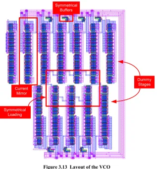
Dummy Stages Current
Mirror
Symmetrical Loading
Symmetrical Buffers
Figure 3.13 Layout of the VCO
The layout of the VCO is employs the basic practices that are standard to reliable analog circuit design. On each side, dummy stages are laid out but not connected. These dummy stages prevent any 'edge effects' from changing the characteristics of one of the stages therefore causing an imbalance.
Another step taken was to make sure that each stage was equally loaded with loading capacitance. To achieve this, equal interconnect between each stage is required, along with the use of 'dummy' buffers, which are not actually connected to any output.
3.1.4 Component: Divide By N
Reset VCO Out
Input to Phase Detector
Figure 3.14 Divide By N Circuit
3.2 System Analysis
The contribution of the phase-detector, loop filter, VCO and divide by N circuit is represented as:
N Kvco s F
Kd ( ) 1
Substituting from the previous equations
N s Kvco s C Ip p 1 1
2π ⋅ ⋅ ⋅
The system equation is now:
Cp Kvco Ip s Cp Kvco Ip s H π π 2 2 ) ( 2+ =
This means, however, that the closed-loop system contains two imaginary poles at
Cp IpKvco s π 2 2 , 1 =±
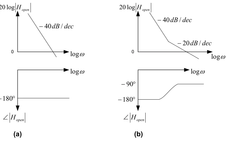
ω log 0 open H log 20 ω log open H ∠ ω log 0 open H log 20 ω log open H ∠ ° −180 dec dB/ 40
− −40dB/dec
dec dB/ 20 − ° −180 ° −90 (a) (b)
Figure 3.15 Phase and Magnitude Response of the PLL
In order to solve this stability problem, it is necessary to introduce a pole into the system. This can be accomplished by adding a resistor in series with the capacitor (Figure 3.15.b). The system equation now becomes
Kvco Cp Ip s KvcoRp Ip s s RpCp Cp IpKvco s H π π π 2 2 ) 1 ( 2 ) (
2+ +
+ =
Which is the open loop system equation. The natural frequency ωn and damping factor ζ can also be found:
Cp IpKvco n π ω 2 = π ζ 2 2 IpCpKvco Rp =
2 2 1 C Cp CpC Rp p + = ω
The effect of this additional pole can be seen in the gain and phase plots in Figure 3.16.
ω log open H ∠ ° −180 ° −90 ω log 0 open H log 20 dec dB/ 40 − dec dB/ 20 −
Figure 3.16 Effect of Ripple Capacitor on Phase and Gain
3.3 System Design
The design of the PLL relies on an understanding of the contributions of the individual functional blocks to the system functionality as a whole. The phase detector gain Kd the gain of the voltage controlled oscillator Kvcothe transfer function of the loop filter
) (s
F and the feedback 1/N can be combined to form a system transfer function.
N Kvco Cp Ip s Rp N Kvco Ip s s RpCp CpN IpKvco s H π π π 2 2 ) 1 ( 2 ) (
2 + +
+ =
0 , 2 1 p = p ω ω , 2 2 1 3 C Cp CpC Rp p + = ω
One zero is also generated by the loop filter.
RpCp z
1
=
ω
The natural frequency ωn and damping factor ζ are also important to the system performance and are given below.
N Cp IpKvco n π ω 2 = N IpCpKvco Rp π ζ 2 2 =
And the loop bandwidth Kloopcan be represented as
N RpKdKvco Kloop=2ζωn =
3.3.1 Determining Design Variables
A circuit designer has control over the following variables in the design process. Kd
Kvco N C Cp
Rp, , 2, , ,
Table 3.1 Fixed Design Variables for the PLL
32
=
N The specification of this PLL called for an output frequency of 172 MHz from a 5.73 MHz clock, this implies that N is fixed at 32 v
MHz
Kvco=119.9 / The low-risk approach of this PLL utilized a ring oscillator composed of single ended inverters. In this case the oscillator is designed to have an output frequency range that is centered at the desired output frequency which is in this case 172 MHz. After designing a VCO to such a specification, the gainKvcois fixed, in this case at 111.9 MHz/v.
pF
C2≅10 Since the loop-filter will be implemented off-chip, there is likely to be significant parasitic capacitance in the i/o pad, the bond-pad and the package lead. Such parasitic capacitance was calculated to be approximately 10pF. Such large parasitic capacitance will most likely make the ripple capacitor unnecessary.
With these values set, it is easier to solve for the remaining variables, a process which employs the use of rules-of-thumb and common-sense to establish the relationship between the system parameters.
3.3.2 Solving the System Equations
It is recommended that the natural frequency be 10 times the input frequency.
in
n ω
ω =10
This relation allows us to solve for the value of Cp. Also setting the damping factor ζ can be assumed to be .8 to preserve stability of the system.
8 .
=
ζ
device capabilities, and is reasonable for the power consumption requirements. In this work, the value of 200µA was chosen as a "first try".
After all the variables have been found, it is necessary to evaluate the system for its stability and performance. It is most efficient to use MATLAB or some other mathematics software package to solve the equations. In this work, MATLAB was used to solve for the system stability and performance using the "control-systems' toolbox. It is not difficult to write a MATLAB program that evaluates the gain-response and response of the feedback system. Through this tool, performance metrics such as phase-margin, and system 'peaking' can easily be measured. The simulation of a PLL at the circuit level is resource intensive, requiring several hours of simulation time to simulate only a few micro-seconds of actual run time. It is therefore necessary to be fairly certain of the system performance before beginning circuit simulations. MATLAB is best used to iteratively change the parameters of the design and view the results. During this iterative process it is necessary to keep in mind several rules of thumb that provide for better system performance and stability.
Table 3.2 Performance Requirements for the System
7 .
>
ζ ωn >10ωin
z
Kloop >4ω ωp >4Kloop
° >65 argin PhaseM
Determine the fixed design variables
Solve for Cs, Cp and Rp
Use MATLAB to calculate the performance metrics
Simulate at the circuit level Meets Performance Criteria Make adjustment Does not meet
performance Criteria Compare with
rules-of-thumb and common sense
Figure 3.17 Process Design Flow
3.3.3 Design Results
MATLAB was used to calculate the gain, phase-margin and stability of the system. After several iterations, the following values were chosen as the most satisfactory for meeting the system requirements.
Table 3.3 Final Values Chosen for Circuit Implementation
Ω =1200
Rp Cp =3nF
F p
C2=10 Ip =250uA
32
=
N Kvco=119.9MHz/v
µ 39
=
Kd
Some of the important system characteristics are shown in Error! Reference source not found.. All the criteria listed in Error! Reference source not found. have been met.
Table 3.4 Performance of Simulated PLL
s rad M
Kloop =1.049 / ωp =83.3Mrad/s
s rad k
z =277.8 /
ω ωn =539.8krad/s
9717 .
=
Figure 3.18 shows the closed loop phase and gain plots while Figure 3.19 displays the open loop gain plots. These graphs, combined with the information in Error! Reference source not found. provides much insight into the performance of the PLL.
103 104 105 106 107 108 109
10-5 100 105
Freq(Hz)
dB
103 104 105 106 107 108 109
-180 -160 -140 -120 -100 -80
Freq(Hz)
De
gr
e
e
s
° =68.85 argin M Phase
Figure 3.18 Plot of the Phase Response of the Simulated PLL
Peaking = 5.26 dB
With a phase margin of 68° the system should be quite stable. A damping factor of .9 also means that there will be no oscillations from a step input to the system, although such a large damping factor means that the system will be a bit slow to respond. One important thing that should be noted from this analysis is the dependence of the circuit performance on the actual value of C2. C2 is responsible for the placement of the third pole. Since at the time of simulation, it was unclear (based on the fact that an off-chip loop-filter was used) what the actual value of C2 would be. A rough calculation yields a value close to 10pF, the value that was used in this simulation. This is a fairly large value for the ripple-capacitor, which places the third pole at a fairly low value. In order to achieve the correct spacing of the loop-bandwidth, natural-frequency and the position of the zero, it is necessary to use a large R*Cp value to place the zero at a fairly low frequency. This in turn causes the damping factor to be large, which results in a stable, but slow-locking phase locked loop.
103 104 105 106 107 108 109 10-5
100 105
Freq(Hz)
dB
103 104 105 106 107 108 109
-180 -160 -140 -120 -100 -80
Freq(Hz)
Deg
re
e
s
C2,Rp Cp,Rp
Rp,Kd
1
2
3
Figure 3.20 Effect of External Loop Filter Adjustment on the PLL
Figure 3.20 shows three vectors 1,2 and 3 that represent the effect of changing the parameters of the PLL. This graph should also give some insight into the benefits of using the off-chip loop-filter to tune the circuit. For example, if the C2 turns out to be much smaller than anticipated, Cp could be reduced and Kd could be increased in order to achieve the best locking-time and stability for the PLL. Likewise, if C2 turns out to be much larger than anticipated, then Cp could be made larger and Rp made smaller in order to preserve a good phase margin.
frequency of the PLL is exactly 32x the input frequency. Figure 3.21 depicts the output voltage at the loop-filter and shows the process by which the loop
Figure 3.21 Circuit Simulation of the PLL Achieving a Lock
self adjusted the control voltage at the loop-filter in order to set the VCO to the desired frequency.
to accommodate process variation. Time was also spent simulating the effects of "powering-up" the circuit, and the effects of varying initial conditions.
After these circuit level simulations were complete, a silicon layout of the chip was completed. Figure 3.22 shows the layout of the PLL with the major blocks identified.
VC0
Phase Detector
Buffer Divide By
N
Charge Pump VCO
GND
PFD Charge
Pump VDD
Clock In
Divide N
PFD GND
Buffer
VDD BufferGND
Filter Output Buffer
Out
VCO VDD
Figure 3.22 Layout of the PLL on the Chip
Table 3.5 Pin Assignments for the PLL
VCO
Phase Detector & Charge Pump Divide By 32
+ 3.3 Volts DC
Buffer
Phase Detector & Charge Pump & Divide by N Buffer
0 Volts DC
VCO Clock In Buffer Out Input and Output Signals
Loop Filter
There were a couple issues that took priority over the layout process. First, it was important to isolate the VCO from the other functional blocks. The VCO is operating at a much higher frequency than the other components and as a result generates 'switching' noise caused by the constant switching of states by the ring oscillator. This is a significant source of noise, and it is important that the other elements of the circuit not be exposed to this. It is also important that the VCO is isolated from the other sources of noise as well. For example, if the VCO were to share a power rail with the divide-by-N circuit you would see a significant voltage ripple on the supply line every 32 cycles when all 8 of the D-Flip Flops switched at the same time. This periodic ripple would actually modulate the frequency of the VCO and would cause a spurious tone to appear at the output of the VCO.
amplitude of the ringing can be large. Large oscillations on either the power or ground rails could prevent the VCO from oscillating and it could reset the values of the flip-flops in the divide-by-N circuit. Isolating the buffer from the other components is commonplace in modern circuit design.
3.4 Fabrication of the PLL
The PLL was one of the designs submitted to Honeywell for fabrication in the MOI5 fabrication in May 2002. The chip was fabricated and returned to NCSU in October of 2002. A package was chosen that accommodated the number of I/O for the chip as a whole, which was then bonded to the die by the technicians at the Jet Propulsion Laboratory. The chips were returned to NC State University in November 2002 to be tested. Figure 3.23 below shows a picture taken at NCSU of the die. One problem that was introduced into this stage was the difficulty in accommodating the large number of I/O pins on the chip. 64 total pins were required, which meant that a package with a large cavity was necessary.
1.02 mm 0.745 mm
Figure 3.23 Picture of the Fabricated PLL
Figure 3.24 Placement of the SOI die in the Package
This large cavity to chip size ratio, necessitates the use of very long bond wires in order to connect the die to the package. These bond wires add series inductance and provide a way for noise to couple to the circuit. The effect of these bond wires on the circuit performance can be observed in the results of the testing.
3.4.1 Testing of the PLL
Several factors greatly complicated the task of verifying the functionality of the PLL. First and foremost was the large series inductance that was introduced by the bond wires and packaging. This series inductance, caused a significant amount of resonance on the power and ground rails of all of the PLL blocks.
-3.5 -3 -2.5 -2 -1.5 -1 -0.5 0 0.5 1 x 10⁻⁸ -1
-0.5 0 0.5 1
vo
lt
age
time
Figure 3.25 Noise on the Power Rail of the Output Buffer
0.9 1 1.1 1.2 1.3 1.4 1.5 1.6 x 10⁻⁷ -2
-1 0 1 2 3 4
volt
age
time
Figure 3.26 Output Signal of the Buffer
Notice that the amplitude of the signal rises and falls above and below the 3.3 voltage limit supplied by the power supply. Also, it is easy to see how the actual pulses vary in their width and shape, indicating that a resonance is taking place that alters the shape of this waveform. Through testing, it was found that the output buffer actually self resonates at frequencies between 120MHz and 135MHz. At self resonance the output waveform became aperiodic and the oscilloscope was unable to track and measure the frequency. This observation is insightful, in that it allows us to make some assumption about the inductive and capacitive elements in the circuit. Using the relation
LC 1
=
ω
We know that for a resonance frequency of 135MHz implies an LC product of
18 3899 .
1 E− . This is a very large number, which implies that either the value of
means that the series inductance of the package and bond wires would be anywhere from 1uH to 69nH. The inductance of a bond wire should be no more than 1nH per millimeter, which means that the series inductance of the bond wires used in this case should be no more than 3nH which means an package and socket inductance of at leas 66nH. This is an unrealistically large number, which implies that there is some parasitic capacitances unaccounted for on the die. Given the highly resistive substrate of SOI, calculating the parasitic capacitances of the metal layers is an exercise in futility. The capacitance
coefficents are so small, that the difference between worst case and best case scenario is a few femto Farads. This leads me to believe that the parasitic capacitance is produced by the packaging and construction of the test fixture.
Figure 3.27 below demonstrated the second problem that complicated the testing process. The signal (between 40mV and 60mV amplitude) is the result of the signal from the output buffer coupling to the other areas of the die. Specifically, Figure 3.27 shows the signal probed at the loop filter, when all the blocks (including the charge pump) are turned on.
-20 -15 -10 -5 0 5
x 10-7
-0.03 -0.025 -0.02 -0.015 -0.01 -0.005 0 0.005 0.01 0.015 0.02
volt
age
time
Figure 3.27 Capacitive Coupled Buffer Noise to other Nodes of the Circuit
relationship implies that the large amplitude and fast rise time of the signal at the output buffer couples capacitively to the substrate and to other areas of the chip.
This capacitively coupled signal prohibits the correct operation of the PLL. The signal in Figure 3.27 comes from the loop filter, probed on-chip. This large amplitude signal overcomes the ability of the charge pump to correctly control the VCO. Instead, the coupled signal at the loop filter causes the VCO to oscillate around 195MHz (as expected since 195MHz implies a control voltage of 0v). This coupling prohibits the PLL from functioning, regardless of the input signal applied. For example, during normal operation, holding the input signal at Vdd (instead of providing the reference clock) should cause the voltage on the loop filter to rise causing the VCO to cease oscillation. Likewise holding the input signal to 0 volts should have the opposite effect. In the presence of the 'coupling noise' holding the input at either Vdd or Gnd had no noticeable effect on either the signal observed at the charge pump, or the frequency observed at the output of the buffer. Such behavior implies that either the charge pump is unable to overcome the effects of the coupled noise, or the coupled noise is so significant that it disrupts the operation of the phase detector or divide-by-N circuits.
These problems dictated the manner in which the PLL was tested. Since the PLL was unable to function correctly as a whole, it was necessary to validate the individual blocks or a combination of those blocks. For example, in order to observe any oscillation from the VCO it was also necessary to activate the output buffer as there were no internal nodes which could be used to observe the output of the VCO. On the other hand, in order to observe the functionality of the charge-pump, phase-detector and loop filter it was necessary to de-activate the output buffer for reasons listed above, and infer the correct oscillation frequency by observing the signal at an internal node of the loop filter.
3.4.2 PLL Testing Results
order to prevent the coupling noise from affecting other areas of the design. Since no output frequency was observable in this configuration, it was
0 0 . 5 1 1 . 5 2 2 . 5 3
0 0 . 2 0 . 4 0 . 6 0 . 8 1 1 . 2 1 . 4 1 . 6 1 . 8
2x 1 0
8
V C O O n ly F u ll P L L S im u la t e d
Figure 3.28 Plots of KVCO Based on Measurements and Simulations
Figure 3.29 Jitter Measurement of the PLL
Error! Reference source not found. shows the results of the VCO jitter measurements. The data indicates that the RMS jitter increases as signal frequency decreases. This is to be expected for a couple of reasons. One, the jitter as a percentage of the period of the signal remains very close.
Table 3.6 Signal Jitter Compared to VCO Control Voltage
Control Voltage
Jitter (ps) Frequency Control Voltage
Jitter (ps) Frequency
0 73.05 200 MHz 1.2 186.6 140 MHz
0.2 96.81 196 MHz 1.4 595.9 120 MHz
0.4 121 190 MHz 1.6 736.8 60 MHz
0.6 165.9 188 MHz 1.8 1046 40 MHz
0.8 132 172 MHz 2.0 1776 20 MHz
With a control voltage of zero, and jitter of 73ps, the jitter is approximately 1.8% of the signal period. A control voltage of 2.2 Volts results in a jitter of 7ns which is
approximately 3% of the signal period, not a large difference over the large tuning range of the VCO. Secondly, as signal frequency is reduced the sampling oscilloscope has a difficult time triggering on the signal, hence making the signal appear somewhat aperiodic. This causes significant deviations in the period of the signal displayed which the scope interprets as timing jitter.
3.5 Conclusions
The goal of this design was to investigate whether or not a frequency synthesizer could be fabricated in the Honeywell SOI process. The results obtained from the testing of the fabricated PLL indicate that this experiment successfully met that goal. A working PLL that was able synthesize the desired frequency (172 MHz) from a low frequency clock (~5MHz) was demonstrated. The charge pump, phase detector, VCO and loop filter functioned much as they did in simulation.
Several new techniques (besides the implementation in SOI) were investigated in this fabrication. The use of an off-chip loop filter, separate power and ground pins for each of the different blocks and an off chip signal driver were new techniques for this research group. The results are mixed.
The use of an off-chip loop filter turned out be functional, but not desirable. The fact that a large series inductance was placed in series with the RC elements of the loop filter resulted in a larger amount of jitter than originally anticipated. Since the fabrication of this chip, more confidence has been gained in the fabrication of passive circuit elements in the SOI process. While accessibility of the loop filter allowed greater insight into the functionality of the PLL, in the future it would be better to trade better performance for accessibility.
PLL made this fabrication worth the money spent. Future designs of frequency synthesizers will most definitely include separate power and ground pins
Bringing the output of the VCO off chip through a large buffer turned out to be a mistake. The amplification of a high frequency signal with large buffers that draw current through highly inductive power and ground lines turned out to cause many more problems then it solved. It would have been a much wiser choice to simply include a probe pad at the output of the VCO so that a high impedance probe could be used to verify its functionality without requiring the noisy buffering that was employed in this design. In the future, any output buffers that are used will employ very, very large decoupling capacitors on-chip on the power and ground rails. Also, any off chip signals will use a reduced swing buffer that will allow the tester to reduce the voltage swing of the output signal to reduce the resonance and signal-coupling problems that were observed in this work.
Chapter 4
Characterization of the Honeywell SOI devices and
circuits
As explained in the introduction, one of the main purposes of the first SOI fabrication was to verify the functionality of the devices and circuits that will be used in the later versions of the frequency synthesizer. To this end, various single MOS devices and ring oscillators were fabricated. The results were collected and analyzed provided insight into the abilities of SOI to be used in RF frequency synthesis. One of the primary goals of this characterization of devices and circuits was to determine the effects of device layout technique on the characteristics of the device and the circuits that utilize them. Device layout technique (explained in Appendix 1) is not modeled for in the device libraries, which adds risk to the fabrication of a chip. It is important to find out before fabrication of the final SOI receiver if (for example) one layout technique is more reliable than another or if one layout technique is more sensitive to process variations or has a large un-modeled parasitic capacitance. These factors will greatly affect the matching or performance of the device. The devices and oscillators that were fabricated for this purpose were not randomly chosen. Each oscillator was designed for a possible implementation in a future RF frequency synthesizer. Different device sizing and layout techniques were used for each oscillator to test different concepts. The size and layout technique of the individual devices was also carefully to resemble the devices that were used in the oscillators.
4.1 Individual Device Characterization
4.2 Design and Layout
For the purpose of characterization, it was necessary to fabricate devices with body tied-to-source (SB) and body independently biased (BT) layout techniques. Figure 4.1 shows examples of the layout of each of these devices.
Body Tied to Source
Body Biased Independently Gate
Drain
Drain Source
Source
Pwell
Pwell P+
P+ Body
Contact
Figure 4.1 Layout of Devices
Pads Drain Drain
Common Source
Common
gate body biasCommon Gate Input Drain 1 Drain 2 Drain 3 Drain 4
Figure 4.2 Arrangement of Devices on the Die
Single Devices
Figure 4.3 Peripheral Location of Individual Devices
The top side of the chip is populated by the SB devices and the right-hand side of the chip is populated with BT devices. Appendix B features a list of the individual devices that were tested.
4.2.1 Individual Device Testing
Figure 4.4 Test Fixture
4.2.2 Individual Device Results
Table 4.1 Performance of Body Biased Devices
Device Type Length Width Performance
PMOS bt 600n 27.75u slow
PMOS bt 600n 13.75u,14u typical>x>slow PMOS bt 900n 18u typical>x>slow PMOS bt 900n 27u slow
PMOS bt 900n 18.5u typical>x>slow PMOS bt 900n 18.5u typical>x>slow PMOS bt 600n 13.5u, 13.5u typical>x>slow NMOS bt 600n 4.4u,4.85u >> fast
NMOS bt 600n 9.25u fast NMOS bt 600n 4.85u,4.4u >> fast NMOS bt 900n 6u >> fast NMOS bt 900n 6u
NMOS bt 900n 6u >> fast NMOS bt 600n 9.25u fast
Table 4.2 Performance of Source Tied to Body Devices
PMOS sb 950n 19u x 4 << slow PMOS sb 600n 27u << slow PMOS sb 900n 18.5u << slow PMOS sb 600n 27.75u slow PMOS sb 900n 18u << slow NMOS sb 600n 9.25u fast>x>typical NMOS sb 900n 6u >> fast
NMOS sb 600n 9.25u typical NMOS sb 900n 6u fast NMOS sb 950n,6u,m=5 fast
Process Corners Revealed
process corner. Figure 4.5 gives a more insightful presentation of that data. On the top the average process corner of the body biased devices appears and on the bottom the average corner of the source - body tied devices are shown.
It was interesting to find that the process variation between the two layout techniques on the same die. While the mean difference between the NMOS and PMOS devices are the same for either of the layout techniques, The 'average' process corner of the body biased devices would be slightly above 'typical' while the average for the source tied devices would be slightly below typical. This wouldn't have too much of an effect on the circuit designer unless they were to 'mix' different layout styles in the same circuit. In which case the circuit would necessarily have to deal with extreme process variation.
Body Biased NMOS Body Biased
PMOS
Source Tied PMOS
Source Tied NMOS TYPICAL FAST SLOW
Figure 4.5 Process Corners of the Fabricated Devices
The ratio of βn to βpwas expected to be between 2.4 and 3 according to the library parameters and simulation. The actual value turned out to be 6 due to a smaller NMOS threshold voltage and a larger PMOS threshold voltage. If circuits were to be mixed with devices of the source tied and body biased layouts, it is possible for a Beta ratio as high as 10. This would be much greater than anticipated by the library and would make oscillator, or any threshold dependent circuits operate poorly.
Variable Threshold Verified
measurement Figure 4.6 shows the results.
0 0.5 1 1.5 2 2.5 3 3.5
10-11 10-10 10-9 10-8 10-7 10-6 10-5 10-4 10-3 10-2
NMOS, l=600n, w=9.25u, A1 2 C2 C2
Gate Voltage D rai n C ur re nt VB=0 VB=.16 VB=.32 VB=.48 VB=6.4 VB=.8
Figure 4.6 Effect of Body Bias on Threshold Voltage
In this experiment, the bias voltage of the body was increased incrementally from 0 to .8 volts. From the graph, it can be seen that the threshold voltage is reduced from a value slightly less than .6 volts to a value of about .3 volts. The subthreshold current slope remains fairly constant throughout this voltage shift, meaning that the device 'off' current is minimized.
Other Observations
one case, the results are consistent across the four chips measured. For the other device, the results vary among the different chips. Such results reinforce the need for process independent layout
4.3 Individual Device Conclusions
The results gathered from the individual devices was useful in several ways. Most importantly, it was verified that the devices are indeed functional and perform more or less close to what was predicted by the models. Secondly, the functionality of the independent body bias for reducing the threshold voltage was verified. Lastly, insight was gained into what can be expected in the actual fabrication environment. Circuits fabricated in this SOI process can not be sensitive to process corners, or on chip process variation. Knowing this information will allow future versions of the frequency synthesizer to be fabricated much more reliably.
4.4 Oscillator Characterization
The ring oscillator serves as the basic building block of the voltage controlled oscillator that would be used in the digital receiver architecture. In this work, the ring oscillators characterized were simple inverter-chain oscillators, configured as shown in Figure 4.7. The oscillator operates on the principle that that a total phase shift of 360 degrees is established around the loop by each stage contributing a phase shift of (negative)
N
/
180° . Additionally, a DC phase shift of 180° is provided by each stage, requiring an odd number of stages in order for the system to be unstable (and therefore oscillate).