ABSTRACT
KIM, HOON SEOK. Advanced Multi Mode Interconnect. (Under the direction of professor Paul D. Franzon.)
Maintaining signal integrity at the dense parallel links and maximizing pin utilization
are the major challenges of interconnect design as the circuit density and computing speed
continually increase. Crosstalk, the noise from the adjacent line, and inter-symbol
interference (ISI), the gain reduction at a high frequency, are the major sources causing
signal integrity problems. Multi-conductor transmission line (MTL) theory provides an
encoding and decoding scheme for cancelling crosstalk at the multi-link channel, and is used
to implement multi-mode interconnect (MMI) that maintains the maximum link-per-pin
efficiency. By using MMI, multiple links can be placed closer together, which saves board
area and lowers the cost. However, MMI induces switching noise because of encoding,
constrains coding, and reduces the flexibility of I/O circuits because it requires
channel-dependent coding at both sides of the transceiver design. In addition, its code sensitivity does
not allow conventional pre-emphasis for reducing ISI and its decoder implementation with
current summing consumes huge power. Therefore, this thesis introduces three circuit
techniques for mitigating the disadvantages of MMI, and also introduces a theory for
improving the flexibility of MMI. The first circuit realizes fractional multi-level
pre-emphasis that reduces the ISI of MMI without breaking its coding scheme. The second
circuit is a digital encoder that reduces the switching noise of MMI drivers. The third circuit
techniques has been implemented in IBM CMOS processes. In addition, a new MMI theory
is mathematically derived for eliminating the decoding requirement so that MMI no longer
powerfully limits the design of receiver-side circuits. This theory is then further simplified so
the theory can be readily implemented as circuits. Finally, a complete transceiver based on
© Copyright 2011 by Hoon Seok Kim
Advanced Multi-Mode Interconnect
by Hoon Seok Kim
A dissertation submitted to the Graduate Faculty of North Carolina State University
in partial fulfillment of the requirements for the Degree of
Doctor of Philosophy
Electrical Engineering
Raleigh, North Carolina
2011
APPROVED BY:
_______________________________ _______________________________ Professor Griff Bilbro Professor W. Rhett Davis
_______________________________ _______________________________ Professor David Schurig Professor J. Michael Doster
DEDICATION
To all the people who have prayed for me since I was born
BIOGRAPHY
I was born in Cheong-ju, Korea, in a family of five, including my parents and two
sisters. My grandfather gave my name to me. My father is a professor at Chung-buk National
University. He has great enthusiasm for education, so I felt the necessity to learn early. My
father is also conservative and strict, so I grew up learning his values. After graduating from
Han-Il, a top high school in Korea, I was admitted to A-jou University with a full scholarship.
I also finished military service as a KATUSA (Korean augmentation troops to the United
States Army), and graduated from A-jou University and Illinois Institute of Technology (IIT)
in a dual degree undergraduate program.
I have been good at math since I was an elementary school student and was the only
student that won the silver badge twice at the math Olympiad. I was also outstanding at
physics and computer science when I was a high school student, so I chose Electrical
Engineering when I advanced to college. I was different from most other high school
students who were only concerned about their school grades. I participated in sports and
earned a black belt in Tae-Gwon-Do. I am still interested in literature and playing guitar. I
have written poems and novels. My GPA reflects my wide-ranging interests. I became more
mature while I lived away from my family in high school, and realized my talent for studying.
I learned teamwork and leadership while I worked in the military as a NCOIC
(Non-commissioned Officer in Charge) at the PAC (Personnel Administration Center) office. Also,
I have a great enthusiasm for learning and researching. The Rotary Club awarded me a
ACKNOWLEDGMENTS
First of all, I would like to extend my sincere thanks to my advisor, Paul D. Franzon,
not only for his endless academic support but also for his unconditional consideration in
person for me throughout the duration of my entire graduate program. This thesis and my Ph.
D program couldn’t have been completed without his incredible inspiration and intuition. It is
my sincere honor that I have studied with him and learned under his care.
I am also thankful to Professor Griff Bilbro, W. Rhett Davis, and David Schurig for
their advisement in the shaping of my research and serving on the committee of my final
defense and preliminary exam.
I am grateful to my co-researcher, Chanyoun, and senior researcher, Yougjin, as well.
They have always been good supporters and friends, and made me enjoy my Ph. D
experience.
I especially acknowledge Dr. Steve Lipa for his instruction in wire bonding and also
for helping me use the lab instruments safely. In addition, I want to take a chance to thank Dr.
Dale for doing FIB service many times without any concern for failures.
I wish the best of luck to all of my lab friends and faculty members who have shared
time with me. The relationships I shared with them will be unforgettable to me for the rest of
my life.
TABLE OF CONTENTS
LIST OF TABLES ... vii
LIST OF FIGURES ... viii
Chapter 1
Introduction ...1
1.1 Interconnect ... 2
1.2 Challenges in High-frequency Interconnect ... 4
Chapter 2
Signal Integrity and Pin Utilization of Off-Chip Interconnect....7
2.1 The Model for Multi-Transmission Lines ... 9
2.2 Inter-Symbol Interference and Equalization ... 11
2.2.1 Inter-Symbol Interference ... 12
2.2.2 Traditional Equalization Methods ... 13
2.3 Crosstalk and MTL theory ... 19
2.3.1 Inductance and Capacitance Model for Multi Lines ... 20
2.3.2 Multi Conductor Lines Theory ... 22
2.3.3 True Matching Termination ... 27
2.4 Pin Utilization of MMI ... 29
Chapter 3
Pre-emphasis Technique for the MMI ... 33
3.1 Channel Model and Coding Coefficients ... 35
3.2 Pre-emphasis Circuit Architecture ... 37
3.2.1 Main Driver ... 39
3.2.2 Digital Encoder ... 40
3.2.3 Fractional Multi-Level Pre-Emphasis ... 42
3.3 Simulation Results ... 44
3.3.1 Switching Noise of Multi-Mode Interconnect ... 44
3.3.2 Switching Noise Reduction of Digital Encoder for Multi-Mode Interconnector ... 46
3.3.3 Signal Integrity Improvement with Pre-emphasis ... 48
3.4 Chip Fabrication and Measurements ... 52
3.4.1 Prototype Implementation ... 52
3.4.2 Measurements ... 53
Chapter 4
Low-Power Advanced MMI ... 56
4.1 Channel Model and Coding Coefficients ... 57
4.2 Advanced Pre-emphasis for MMI ... 58
4.2.1 Circuit Architecture ... 60
4.2.2 Simulation Results ... 61
4.3 Low-power Decoding Receiver ... 65
4.3.1 Circuit Architecture ... 66
4.3.2 Simulation Results. ... 69
4.4 Chapter Conclusion ... 72
Chapter 5
Transmitter-Encoding MMI Theory ... 73
5.1 Transmitter Encoding Multi-Mode Interconnect Theory ... 74
5.1.1 Conceptual Representation ... 75
5.1.2 Mathematical Representation ... 77
5.2 Block Level Implementation ... 81
5.3 Channel Model ... 85
5.3.1 Channel Response ... 86
5.3.2 Lumped Model of Channel and Termination ... 87
5.4 Voltage Mode Simulation with Ideal Source ... 89
5.4.1 Conventional Single-ended Interconnect Case ... 90
5.4.2 Multi-Mode Interconnect Case ... 91
5.4.3 Transmitter Encoding Multi Mode Interconnect Case ... 93
5.5 Current Mode Transmitter Encoding Multi-Mode Interconnect Implementation and Simulation ... 96
5.5.1 Delay Control Circuit ... 97
5.5.2 Driver Circuits ... 99
5.5.3 Termination ... 101
5.5.4 Jitter and Power Supply Noise Immunity Analysis ... 103
5.6 Chapter Summary ... 105
Chapter 6
Contribution and Future Tasks ... 107
6.1 Contribution ... 107
6.2 Future Tasks ... 109
REFERENCES ... 111
APPENDICES ... 114
Appendix A: Matlab Code for Codes and Termination Impedances ... 115
Appendix B: Pre-emphasis Circuit ... 116
LIST OF TABLES
Table 2-1: Performance comparison of various interconnects. ... 32
Table 3-1: The characteristics of equalizing techniques. ... 34
Table 3-2: Signal integrity improvement of proposed pre-emphasis ... 51
Table 4-1: Numerical data of signal integrity comparison. ... 64
Table 5-1: Weightings and 16 assigned inputs for each driver. ... 84
Table 5-2: Required delay setup for all input ports. ... 93
Table 5-3: Input setup for voltage drivers. ... 93
Table 5-4: Jitter analysis for timing error. ... 95
LIST OF FIGURES
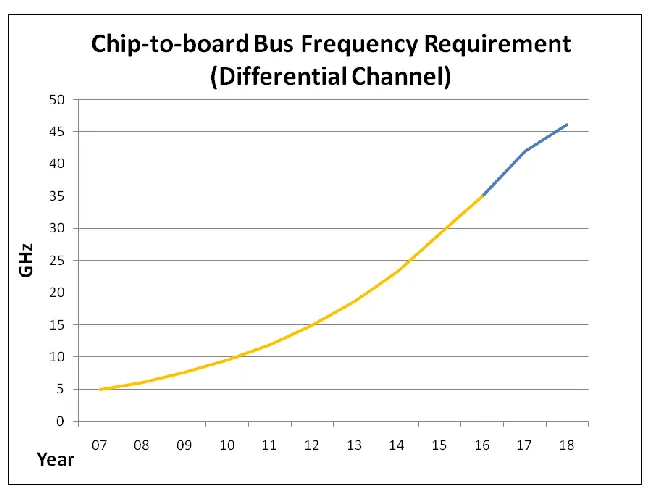
Figure 1.1: Off-chip bandwidth requirement graph. ... 4
Figure 2.1: Basic interconnect diagram. ... 7
Figure 2.2: (a) Lumped model for the transmission line (b) Lumped model for double lines. ... 9
Figure 2.3 : Frequency responses for four embedded striplines. ... 11
Figure 2.4: Transient response of channel showing ISI. ... 12
Figure 2.5: Flattening frequency response of a channel by the equalizer. ... 13
Figure 2.6: Three-tap pre-emphasis circuit diagram. ... 14
Figure 2.7: Receiver side FIR filter. ... 15
Figure 2.8: Rx Continuous time equalizer. ... 16
Figure 2.9: Decision feedback equalizer. ... 17
Figure 2.10: Four conductor transmission lines model. ... 20
Figure 2.11: Block diagram of MMI. ... 26
Figure 2.12: True matching termination for MMI. ... 28
Figure 2.13: (a) Increasing ratio of CPU internal clock speed and number of cores and (b) On-chip frequency × number of total cores... 29
Figure 2.14: Number of total package pins. ... 30
Figure 3.1: Cross-sectional dimensions and S-parameter response of channel bundle. ... 35
Figure 3.2: Block diagram for Tx-side. ... 37
Figure 3.3: Tx design for generating 5 levels. ... 39
Figure 3.4: Encoding demonstration ... 40
Figure 3.5: Encoder logic and the truth tables for each level. ... 41
Figure 3.6: (a) Pre-emphasis controller (b) Pre-emphasis drivers. ... 42
Figure 3.7: Data jitter comparison between single-ended mode and MMI due to switching ... 45
Figure 3.8: Reduced data jitter at the far-end transmission line by using a digital encoder at 2 Gsymbol/s. ... 46
Figure 3.9: Data jitter analysis for digital encoder. ... 47
Figure 3.10: Multi-level eye diagrams and data jitter analysis at the receiver side. .... 48
Figure 3.11: Eye diagram and jitter analysis of ideally restored signals on Rx-side. .. 49
Figure 3.12: Graphical summary of pre-emphasis performance. ... 50
Figure 3.13: Pre-emphasis design layout and test board. ... 52
Figure 4.1: Cross-sectional dimensions and S-parameter response of channel bundles.
... 57
Figure 4.2: Entire circuit map for previously designed pre-emphasis. ... 59
Figure 4.3: Pre-emphasis block diagram and circuit. ... 60
Figure 4.4: Jitter for normal single-ended mode. ... 61
Figure 4.5: Signal Integrity of MMI without pre-emphasis. ... 62
Figure 4.6: Signal Integrity of MMI with pre-emphasis. ... 63
Figure 4.7: Current summing decoder. ... 66
Figure 4.8: Three-stage decoding concept. ... 67
Figure 4.9: Differential source follower-decoder and differential to single-end converter. ... 67
Figure 4.10: Decoding procedure. ... 68
Figure 4.11: Signals at each stage of decoder ... 69
Figure 4.12: Jitter of MMI Transceiver ... 70
Figure 4.13: Layout for low-power MMI. ... 71
Figure 4.14: Advanced MMI design overview. ... 72
Figure 5.1: Block diagram for Tx part of Tx encoding MMI. ... 83
Figure 5.2: (a) Cross sections and port assignments of the channel bundle; (b) frequency responses ... 86
Figure 5.3: Pi-model resistor termination tree. ... 88
Figure 5.4: Single-ended case eye diagram and jitter (a) with 50 Ω termination and (b) with pi-model termination at the far end transmission line. ... 90
Figure 5.5: Eye diagram and jitter of the MMI ... 91
Figure 5.6: Phase differences of each line. ... 92
Figure 5.7: Voltage mode simulation setup. ... 94
Figure 5.8: Eye diagram and jitter of Tx encoding MMI. ... 95
Figure 5.9: Block diagram for circuit implementation. ... 97
Figure 5.10: Multi-level driver for one link. ... 99
Figure 5.11: (a) Signal and noise swing when Vdd2 is 1.2 V (b) SNR ratio caused by the unbalanced switching time by Vdd2. ... 100
Figure 5.12: Approximated termination impedance for the MMI. ... 101
Figure 5.13: (a) Reflection with 50 Ω termination and (b) reflection ratio by termination impedance. ... 102
Figure 5.14: Data jitter and noise generator. ... 103
Figure 5.15: Data jitter of circuit level Tx-encoding MMI (a) without data jitter (b) with data jitter and supply voltage noise ... 104
Chapter 1
Introduction
The development of computers was a revolutionary event in our society. The
computer has continuously improved its computing speed since it was developed. Now,
computers solve extremely complex problems, saving humans the effort, and store huge
amounts of data without filling an entire building with paper boxes. The decrease in
manufacturing costs of silicon chips introduced the era of personal computers, and now
people cannot imagine living without one.
In recent times, people prefer faster and more functional computers, so the
chip-to-chip data transferring speed requirement has already reached terabits per second [13] while
the chip size has continually decreased. Also, a low-power circuit design is required due to
the high demands of portable electronic devices using batteries for their power supply.
Therefore, the modern I/O circuit design has to satisfy the requirements of wide bandwidth
up to high frequency while using a small number of pins and consuming small power.
Because of these requirements, I/O circuit design has become very complex and requires
1.1 Interconnect
Interconnect is an I/O circuit design for transmitting and receiving data over wired
lines. For example, it can be used for cables, PCB traces and metal layers inside a chip. It is
also known as the transceiver design, which means transmitter and receiver design. Its
applications are everywhere between circuits in any system due to the fact that data
communication is necessary for all systems. Hence, if the system speed increases, the amount
of data transferred between systems also increases.
There are two ways to increase the data rate of systems. One way is to increase the
transferring bit-speed over the line, and another is to make more parallel links. However,
high-frequency links have several factors causing bit errors, and the parallelization is also
limited by the reduction of chip size, limited area and pin count. Therefore, wider bandwidth
and more parallelization are the simultaneous requirements of an interconnect scheme.
One of the most important factors to consider in the high-frequency and parallel
interconnect design is signal integrity. Low signal quality carries a higher risk for errors even
though some errors can be corrected by error detecting and correcting algorithms.
There are two major factors that degrade signal quality. One is inter-symbol
interference (ISI), which is noise coming from the subsequent bits on a single wire. It is due
to the frequency-dependent loss of the imperfect conductor. Another is crosstalk, which is
noise coming from adjacent links. These two issues significantly degrade the signal quality
by narrowing the unit interval (UI) and reducing the swing of the signal in multi-giga or
severe at dense links [2]. If the UI or swing of a signal gets too narrow or small due to noise,
1.2 Challenges in High-frequency Interconnect
The bandwidth requirement for the interconnect design has continually increased.
Figure 1.1 shows the rising increments of bandwidth requirement for off-chip data
communication by year [3]. This requirement cannot be solved even with cutting-edge serial
interconnect schemes. The blue line indicates the unachievable bandwidth with current
differential mode interconnect design technology [3]. Hence, a wide bandwidth interconnect
design in multi-giga range with more parallelization is inevitable for future interconnect
designs.
The major challenges of future interconnect designs are reducing crosstalk and ISI
noise in order to achieve higher speed and more parallel signaling while maintaining the
power and pin-per-link efficiencies. By eliminating crosstalk noise and ISI, data jitter and
signal swing uncertainty can be reduced. In addition, the broad usages of portable devices
strongly require low-power designs for the entire electrical system including interconnect.
The multi-mode interconnect (MMI) design concept is selected in this thesis to
completely cancel crosstalk at high frequencies on multi-link channels [1]. The MMI design
is chip-to-chip and multi-link interconnect implementation based on the multi-conductor
lines (MTL) theory [4]. Encoding and decoding is the suggested solution for the crosstalk
cancellation. It theoretically guarantees perfect crosstalk cancellation at uniform transmission
lines and maximum link-per-pin (link / pin) efficiency. However, the coding sensitivity for
cancelling crosstalk limits the design flexibility. The equalizer design for reducing ISI
becomes especially complicated.
Therefore, three advanced design concepts are presented for enhancing the previous
MMI. The first design concept is a fractional pre-emphasis and a digital encoder. These two
designs reduce the ISI and switching noise, respectively, by equipping them on the
transmitter-side of MMI. The second design concept is a low-power design concept for MMI.
The previous MMI design wastes a lot of power especially on the receiver-side, so the source
follower decoding receiver (Rx) is proposed for reducing power on the Rx-side. The third
design concept is an advanced MMI design based on modified crosstalk cancellation theory
requirement of the precious MMI so it increases the design flexibility of the Rx-side circuit
for employing equalization circuits and amplifiers.
As data rates increase up to multi-gigabits-per-second, data jitter becomes the critical
noise source. Research shows that crosstalk noise is the dominant data jitter source at dense
links, and crosstalk reduction is necessary to improve signal integrity. Also, the crosstalk
cancellation and maximum link / pin efficiency of MMI allows saving board area and the
required number of pins, and thus the costs associated with them. Furthermore, ISI and
switching noise mitigation techniques are introduced for suppressing data jitter at
high-frequency signaling. The power efficiency of interconnect considering the limited battery life
Chapter 2
Signal Integrity and Pin Utilization
of Off-Chip Interconnect
The main goal of chip-to-chip interconnect is successful digital data transmitting and
receiving through wired channels. The signal integrity is the signal quality estimation of
received signals. The various noise and mismatched time-synchronization in circuits disturb
the desired signals and reduce the signal quality. Signal integrity is commonly estimated by
data jitter and voltage swing of the eye-diagram or bit error rate (BER) measurement.
Basic interconnect design is composed of Tx, channel and Rx. It is shown as a
diagram in Figure 2.1. The Tx generates signals and drives the channel, and various
modulation techniques can be applied on the Tx-side. In the case of MMI modulation, the
encoding is necessary, so it can cause additional switching noise while conducting encoding.
If the channel is a multi-link and mismatched timing synchronizations are induced among
links on the Tx-side, significant data jitter can be presented while the signals go through the
channel. The conventional channel is composed of copper lines that are partially or entirely
surrounded by dielectric materials. This channel is lossy and has frequency-dependent
response since the conductor is non-ideal. ISI is due to this frequency-dependent response
which acts like a low-pass filter. Crosstalk noise will be added if the channel is a dense
multi-link, and the data rate is multi-giga or higher bits-per-second (bps). The final stage is the Rx
which detects the signals and restores the transmitted signals by demodulating or isolating
signals from various noises. The ideal interconnect having high signal integrity guarantees
the perfect match between initial digital data and restored digital data.
Typically, the transceiver is designed to have low BER, a wide and tall eye-diagram
or small data jitter on the given channel. Therefore, the analysis of channel characteristics is
an important portion of interconnect design. Otherwise, the interconnect cannot be designed
efficiently to overcome the disadvantages of a given channel. This chapter describes the
channel characteristics of a multi-link, associated techniques and MTL theory to compensate
2.1 The Model for Multi-Transmission Lines
PCB traces used for the multi-giga bps and chip-to-chip interconnect are treated as
transmission lines because the parasitic components of wires cannot be ignored. The
transmission line is conventionally considered as the lumped RLGC model shown in Figure
2.2(a), so it has low gain at high frequencies because of its L and C components [5]. The
well-known telegrapher’s equation explains the propagating relations between the signals at
each end of the transmission line, and defines the characteristic impedance, , by the ratio of
the voltage and current through the line.
R
L
G
C
(a)
L
L
Lm
Cm
C
C
R, L, G, and C are the resistance per unit length, inductance per unit length,
conductance of the dielectric per unit length and capacitance per unit length, respectively.
The lumped RLGC transmission model can be duplicated identically for multiple
transmission lines. However, if multiple transmission lines are placed closely to each other,
the lumped models have to include not only the frequency-dependent gain but also the
crosstalk relations between neighboring lines for accurate channel response analysis. The
crosstalk relation is conventionally explained as mutual inductance and mutual capacitance
for the given distance between transmission lines due to its frequency-dependent
characteristic coming from the magnetic and electric fields between lines [6]. The model for
two-coupled transmission lines is shown in Figure 2.2(b). Lm and Cm indicate mutual
2.2 Inter-Symbol Interference and Equalization
Frequency-dependent gain of the transmission line is mostly due to the skin effect and
dielectric loss [7]. The skin effect is a phenomenon where high-frequency currents tend to
flow only through the surface of the conductor. Thereby, it increases the effective impedance
at a high frequency and the self-inductance impedance of the conductor as well. It tends to
increase proportionally to the square root of the frequency. Dielectric loss is due to the
energy loss through the dielectric material, and it increases proportionally to the frequency.
This frequency-dependent gain is also shown on multi-line channels. The overall
frequency responses from 1 kHz to 20 GHz of five-centimeter-long four embedded striplines
are plotted in Figure 2.3. It shows the ratio of delivered energy over transmitted energy for all
four lines. It indicates that the amount of delivered energy proportionally decreases by
frequency in dB scale, and the loss graphs are identical for all four lines because they are all
2.2.1 Inter-Symbol Interference
Due to the low channel gain at a high frequency, the high speed signal is disturbed by
the previous signals. This noise is called ISI. This phenomenon is also observed from the
transient channel response in Figure 2.4. Embedded striplines illustrated in Figure 2.3 were
used for the simulation.
Figure 2.4: Transient response of channel showing ISI.
The sharp signal edges spread out while the signal propagates through the conductor
line. The signal edges contain the highest frequency components, so their slopes decrease
2.2.2 Traditional Equalization Methods
The equalizer is a specialized circuit scheme to reduce the ISI. The equalizer flattens
the frequency response of a channel for increasing the achievable data rate. The conceptual
graph in frequency domain is shown in Figure 2.5. The conventional equalizer reduces the
low frequency gain and adds the high-frequency gain to flatten the frequency response [9].
Figure 2.5: Flattening frequency response of a channel by the equalizer.
The Equalizer can be implemented either on the Tx-side or Rx-side. It is also
implemented on the both sides for further signal integrity improvement [10]. The
equalization on the Tx-side is typically a finite impulse response (FIR) filter using
equalization tap coefficients. Taps reshape transmitting signals to attenuate low-frequency
portions and to emphasis high-frequency portions according to the determined coefficients.
This method pre-distorts the transmitting signal so ISI and pre-distorted components can be
canceled out through the channel. Due to this, it is referred to as pre-emphasis circuits and
The coefficients are determined based on the estimated ISI of a channel. Increasing
the number of taps can eliminate more ISI but increases the power and reduces voltage swing.
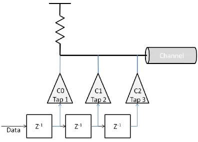
Figure 2.6 shows the diagram for a three-tap pre-emphasis circuit. Data delay between
adjacent taps is one unit interval (UI). The first tap is a main driver which generates the
voltage or current level along with the digital values of data. The other two taps reshape the
signal driven by the first tap so it compensates with ISI through the channel [11][12].
The conventional pre-emphasis is uncomplicated to design even at a high frequency
since it is easy to control the delays of the digital signals. Its major advantage is that it does
not amplify or feed noise back to the signal. However, it reduces the low-frequency gain, so
this method may not suitable for equalizing encoded signals.
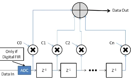
In a manner similar to FFE on the Tx-side, the Rx-side equalizer can be implemented
as a FIR filter in either analog or digital way (Figure 2.7). The analog Rx FIR filter is
required to design an analog signal delay cells which are difficult to achieve tap precision
[14]. On the other hand, the digital Rx FIR filter is required to use the analog to digital
converter (ADC) for digitizing the input. The resolution of an ADC determines the
performance of the equalizer. High-resolution ADCs make tap coefficients precise. However,
an ADC with high-resolution and speed consumes a lot of power. In addition, it has the
potential risk of amplifying and feeding back other noises.
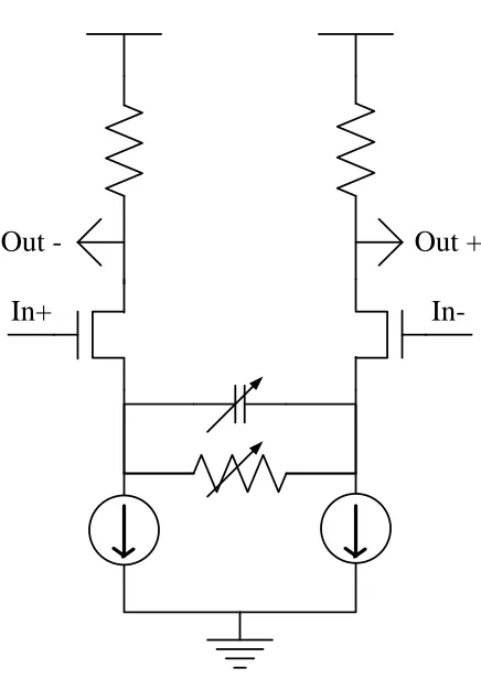
An Rx-side equalizer commonly implemented as a continuous time active filter is
shown in Figure 2.8 [15][16]. This filter has passive components to produce the
high-frequency gain. The major constraint of on-chip passive components is the adaptability
according to the limited space. Achievable compensation gains are strongly limited by the
space. This technique is usually used at the first stage of a receiver which is generally a
common source amplifier with frequency-dependent source degeneration.
In+
In-Out - Out +
A decision feedback equalizer (DFE) is another Rx-equalization technique [17][18].
It is a nonlinear equalizer illustrated in Figure 2.9. The DFE digitizes input signals and
amplifies only signals so it is broadly used in high-speed interconnect. It decides the amount
of ISI to remove from referencing the past decision. However, if the slicer makes a wrong
decision, it can keep cascading detection errors. Additionally, a clock and data recovery
(CDR) circuit is required prior to the DFE functions.
The traditional equalizers reviewed so far consider only ISI. However, crosstalk noise
becomes severe when the data rate and the parallelization increase. Therefore, new
techniques are needed which are compatible with crosstalk-canceling techniques. In the next
section, crosstalk and the method for canceling it will be introduced prior to exploring the
2.3 Crosstalk and MTL theory
Crosstalk is the noise originating from the intercommunication between neighboring
signals at high frequencies when the signaling lines are placed in close proximity to each
other. Electric and magnetic fields are generated while the signal propagates throughout
transmission lines, and these fields affect adjacent conductor lines. These relations between
coupled transmission lines are typically illustrated as mutual capacitance and inductance
2.3.1 Inductance and Capacitance Model for Multi Lines
The lumped model for single and double transmission lines were shown in Figure 2.2.
In a manner similar to them, the lumped model for more lines can be expanded by
considering the mutual capacitances and inductances among all of the other lines. Figure 2.10
shows the lumped RLGC model for four lines.
L33
3
4
G
L44 L111
2
L22 Cm12G
8
7
6
5
Lm12 Lm23 Lm34 Lm13 Lm24 Lm14 Cm23 Cm34 Cm13 Cm14 Cm24 C44 C33 C22 C11Figure 2.10: Four conductor transmission lines model.
All Lm and Cm components indicate the mutual inductance and capacitance
components of multi-transmission lines, respectively. These mutual factors can be modeled
as a matrix form by combining them with the self-inductances and self-capacitances of the
Diagonal components represent self-inductance and self-capacitance of each line, and
non-diagonal components represent mutual inductances and mutual capacitances between
lines. Then, the current and voltage relations of n coupled-lines can be also defined, as a
matrix forms from the and matrices by Lenz’s law.
2.3.2 Multi Conductor Lines Theory
The telegrapher’s equation defines the relation between the near-end voltage and
current of the transmission line, and the far-end voltage and current of the transmission line
by solving the wave equation. This can be expanded to multi-transmission lines. Let R, L, G,
and C be defined as n × n matrices containing mutual inductances and capacitances between
n coupled-lines.
For solving this differential equation, (2.1) and (2.2) need to be differentiated with
respect to line distance, x.
And then, substitutes
of (2.3) with (2.2) and of (2.4) with (2.1),
respectively:
In the steady-state state, can be substituted with [29]:
Let be defined as a n × n square matrix of , and as a n × n square matrix
of , then the MTL equations are defined as [19],
where and are an n × 1 column vectors for the voltages and current, respectively, of n
conductor lines. If the transmission lines are lossless or have ignorable loss, these
second-order differential equations can be rewritten as substituting R and G with constant zero.
There are two important notices in these equations. Unless and are diagonal,
all the signals at the far-end transmission lines are related to each other by mutual
inductances and capacitances between transmission lines. Although the mutual inductance
and capacitance values are determined, each signal at the end of the channel bundle depends
on not only one input but also all the other neighboring inputs.
Therefore, the complicated relations between the inputs and outputs of multi-link
channels can be explained as modes, which is the harmony between input combinations and
channel characteristics. MTL theory illustrates this complex multi-line signaling as the
combination of fundamental modes of each line [4][19]. Multi-mode interconnect is the
modal signaling scheme that uses these fundamental modes for isolating each line from the
adjacent lines.
In essence, the characteristic of n-line channel signaling can be explained with n
fundamental modes. The relations between inputs and outputs are complicated because these
fundamental modes are combined according to a certain rule by the input combinations and
the characteristics of the channel bundle. Thus, MTL theory suggests the modal
decomposition method for canceling crosstalk, which transforms the n × n and matrices
to a diagonal matrix of n eigenvectors. It means that each transmission line propagates the
signal as a fundamental mode without any of the effects of mutual inductance and
capacitance from the adjacent signals.
For eliminating crosstalk-related terms of or from the equations (2.5) and (2.6),
the modal decomposition method is used, which multiplies a converting matrix, either or
Then, natural voltage and natural current are transformed as ,
and . If the MTL theory is correct, fundamental mode signaling can be achieved
by adapting an inverse modal combination throughout the entire signal sequence through the
channel.
Since and are constant matrices
If and are invertible, the left-hand side of equations can be simplified as
Where and are referred to as modal voltage and modal current when and
become diagonal by and , respectively, with LDU decomposition formula.
and are the physically transmitted natural voltages for the voltage mode circuit
and transmitted currents for the current mode circuit respectively in circuits. The relation of
and is defined as = .
The diagonal matrices, and are noted as and , and
the eigenvector, is the propagation constant of transmission lines.
When this MTL theory is implemented as a circuit called MMI, the encoder performs
on the Tx-side and the decoder performs on the Rx-side. Figure 2.11 shows the
block diagram of MMI.
2.3.3 True Matching Termination
If the transmission lines are considered as lossless or their losses are negligible, the
characteristic impedances for n lines are calculated by the ratio of the self-inductance and the
self-capacitance of each line. They have the same ratio as the traveling voltage and current on
each conductor line.
However, this termination is not ideal for multi-coupled transmission lines since it
has mutual inductances and capacitances between each line. The cross-coupled voltage and
current relations make the single signal-to-ground termination flawed. Therefore, the true
matching termination for multi-coupled transmission lines is defined as an n × n matrix
according to the MTL theory [20].
This matrix form can be represented as a pi-model or T-model resistor tree. Pi-model
Figure 2.12: True matching termination for MMI.
The physical resistance values for the pi-model are calculated by the equation below
[20]:
By using the true matching termination, most of reflection can be theoretically
2.4 Pin Utilization of MMI
Although crosstalk and ISI can be mitigated on high-speed interconnect by the MTL
theory and equalization technique, there is still another constraint for interconnect design. It
is the lack of the number of input and output (I/O) pins. Figure 2.13(a) shows the increasing
ratio of the internal clock speeds of central processing units (CPUs) and the number of cores.
Figure 2.13(b) shows effective data computing frequency which is a multiplication of
on-chip frequency and the number of total cores [3]. The increase in the number of cores boosts
the computing speed dramatically and produces the demand for a huge amount of off-chip
data transfer. For example, PlayStation 3 has a multi-core system with a 3.2 GHz internal
clock frequency and it requires a 25.6 Giga-byte-per-second off-chip data transfer from the
CPU to memory [30]. This amount will increase linearly by the number of CPU multiplied
by the internal clock frequency if the multi-core controlling algorithm can maximize the
performance of multi-core system.
However, the number of total package pins increases only by 7.5% each year, even
though the pin size is being reduced to increase the number of pins (Figure 2.14) [3].
Figure 2.14: Number of total package pins.
Hence, link / pin efficiency should be considered for the future of interconnect.
Several crosstalk-canceling or noise-reducing multi-link interconnects having improved link /
pin efficiency have been introduced so far. Most designs were not able to cancel the crosstalk
completely, but only to reduce or partially cancel it while they improved link / pin efficiency.
Hae-kang Jung showed the data jitter reduction scheme by adjusting the delay of
transmitting data, which mitigates the major propagation delay differences between each line
of the channel bundle [21].
Kwang-Il Oh suggested an alternate data-transmitting scheme between the closest
lines for minimizing the risk of crosstalk so that if one signal makes the transition on a link,
the crosstalk-induced signal can mostly affect the middle of the bit period for neighboring
Kyungho Lee proposed a crosstalk reduction scheme by adjusting the capacitance
value of the middle transmission line among three lines. Intentional curves are added to the
middle trace for adjusting the related capacitances with the middle trace, so crosstalk-related
or of channel bundle can be close to a diagonal matrix [23].
Youngsik Hur presented the near-end crosstalk-cancelling method for four-level pulse
amplitude modulation (PAM) signals. It detects the near-end crosstalk from the neighboring
line and equalizes this noise with an equalizer on the Tx-side [24].
Sotirios Zogopoulous’s design did not contribute to cancelling crosstalk, but
exhibited a three-level differential coding scheme for reducing ISI and switching noise and
increasing the pin utilization of differential signaling from an 0.5 link / pin to an 0.75 link /
pin. It used three levels instead of two levels for differential signaling and kept the same
average voltage of four lines so the interconnect could have a robust DC bias level. However,
there was no specified scheme to reduce or cancel the crosstalk [25].
A crosstalk amplitude-cancelling method using code division multiple access (CDMA)
was suggested by Tzu-Chien Hsueh, as well [26]. It could reach up to 0.75 link / pin for a
four-pin channel by multiplying orthogonal codes to the data, but this method required the
extra bandwidth for coding. The baud rate had to be twice the frequency of the data rate
because of the required frequency for mixing codes to the signals. In addition, if each line has
significant propagation-delay difference with others, the orthogonal coding method will be
flawed since the CDMA coding technique is only for signal merging and not for eliminating
the propagation delay differences between lines. Table 2-1 shows a summary of these
Table 2-1: Performance comparison of various interconnects.
This table illustrates that the MMI is only interconnect scheme promising complete
Chapter 3
Pre-emphasis Technique for the MMI
Although the MTL theory is a promising theory for crosstalk cancellation at high
frequencies, ISI reduction is not considered at all. Nevertheless, the previous MMI did not
include any circuit schemes to reduce the ISI. It is hard to adapt conventional equalizing
techniques because of the coding constraint and extremely noisy signals at the Rx-side.
The MMI needs to have multi-level signaling because of the encoding, and each level
must be protected for efficient crosstalk cancellation because MMI relies solely on encoding
and decoding accuracy for crosstalk cancellation. However, the conventional Tx-side
equalizer breaks the encoding codes, and the Rx equalizer amplifies or feeds back the
crosstalk noise. The types of conventional equalizers are summarized, and the considerable
characteristics of each type of equalizer are illustrated as well in Table 3-1.
The Rx FIR equalizer risks amplifying the input signals without filtering all other
noises except for ISI. It can be a critical risk for MMI since it can amplify the crosstalk
before the decoding occurs. In addition, the signals on the Rx-side are quite noisy and
multi-level, so the risk increases.
DFE is also hard to equip to MMI because of requirements of symbol-to-symbol
propagation delay with other lines, and DFE consumes a lot of power in the case of using
high speed ADC. In addition, DFE has to be equipped after decoding since it is hard to
estimate the multi-level signals at the end of lines before the decoding occurs.
A Tx FIR filter carries risk as well because it causes level distortions of signals for
compensating ISI. However, the level-distortion can be negligible by the proposed
pre-emphasis scheme called fractional and level selective pre-pre-emphasis. The new pre-pre-emphasis
design basically protects the signal levels of MMI for preserving crosstalk-free conditions
while increasing the high-frequency gain and reducing the switching frequency of
transmitting signals for better signal quality.
3.1 Channel Model and Coding Coefficients
A proposed pre-emphasis circuit is adaptable for four conductor-lines, having
identical mutual distance from the center of the channel bundle to each conductor. The
dimensions of the transmission line model used for the simulations and R, L, G and C
matrices for transmission lines extracted by the Hspice field solver are shown in Figure 3.1.
A thirty-centimeter-long RLGC model was used for the simulation. The embedded striplines
with light crosstalk were used so the multi-level protection could be observed clearly at the
Rx-side without adapting decoding.
3 2 4 1 GND GND 1.4mil 1.4mil 5mil 1.4mil 5mil 1.4mil 5mil 5mil 5mil 5mil Reference plane Reference plane Signal wire(Cu) Signal wire(Cu) 16.4mil
εr = 4.25, tanδ = 0.016
The encoding and decoding matrices, and , for this channel bundle were
calculated based on the MTL theory which was introduced in the previous chapter. Matrices
can be multiplied or divided with any constants, since it doesn’t affect the decomposition of
the or matrix.
The termination-impedance matrix, was calculated from equation (2.7) as well.
50 Ω, single line-to-ground terminations (≈ 52.87 Ω) were used for this simulation
since the diagonal impedance terms were dominant and non-diagonal impedance factors were
insignificant. Matlab was used for finding encoding and decoding coefficients, and
termination values from the extracted L and C matrices. The Matlab script is attached in
3.2 Pre-emphasis Circuit Architecture
The major circuits for the proposed Tx-side of MMI are the digital encoder, fractional
multi-level pre-emphasis circuit, and driver. The digital encoder re-orders the encoding
matrix so that the switching frequency can be minimized. If the initial input combinations
result in the same level after encoding, the outputs of the digital encoder maintain its bit
status in order to prevent the unnecessary switching of drivers. The pre-emphasis circuit
fractionally generates inverse energy against ISI for suppressing ISI and protecting the
encoding coefficients simultaneously. The driver handles the channel bundle so that each line
can have five different levels. The multiplication of the encoding matrix and binary signal
vector makes five different levels for each line of a given channel bundle. Figure 3.2 shows
the block diagram of the entire Tx-side design. All circuits were designed in IBM 0.13 µm
The digital encoder encodes 4-bit binary inputs to 4 pairs of 4-bit binary outputs. All
outputs are duplicated once so there are two identical output sets for the digital encoder. One
set becomes the inputs of the pre-emphasis weighting and timing controller. The outputs of
the pre-emphasis weighting and timing controller make 4-bit low-to-high pulses and 4-bit
high-to-low pulses per link depending on its input switching direction. These pulses operate
the pre-emphasis drivers for enhancing the switching speed of the main driver so that it can
overcome the ISI. The other set is connected to the gates of the NFET-driver. The input set
for the main driver is delayed as much as the propagation delays of the pre-emphasis
controller so that the driver and pre-emphasis drivers can be synchronized. All of the circuit
3.2.1 Main Driver
Single-ended saturation-NFET current mode drivers were used for driving the
channel bundle on the Tx-side. The five required current levels were generated by turning on
or off four pulling-down sub-drivers. Figure 3.3 shows the schematics of the driver for one
link. The same drivers are used for all other links.
VDD
TL
Encoded inputs 5 levels
3.2.2 Digital Encoder
The previous encoding scheme of MMI was just routing from initial non-return zero
(NRZ) binary data and inverted data to sub-drivers that were weighted by encoding
coefficients [1]. This method followed the matrix calculation steps exactly, as will be
demonstrated in Figure 3.4.
Therefore, there is always one switching sub-driver per link whenever one input
changes, even though multiple input changes result in the same driving strength on a line. In
the case of Figure 3.4, the signal on the 4th line maintains the same level when the input
vector changes from to , but three sub-drivers connected to the 4th line will be
switched by this input change.
The proposed digital encoder prevents the unnecessary driver switches. All
sub-drivers will not switch if the input combinations induce the same level after encoding. The
detailed logic of the digital encoder and its truth table for T of equation (3.1) are shown in
Figure 3.5. The same digital encoder circuit is used for all four links. However, input orders
3.2.3 Fractional Multi-Level Pre-Emphasis
Pre-emphasis circuit is divided into two parts: controllers and pre-emphasis drivers.
The controller part detects input changes of each sub-driver and generates adequate pulses to
control the emphasis drivers to reshape transmitting signals against ISI. The
pre-emphasis drivers are composed of 16 PFETs and 16 NFETs. There is one PFET and one
NFET for each current mode sub-driver. NFET-pre-emphasis enhances pulling-down
currents when the current mode sub-drivers are turning on, and PFET-pre-emphasis disturbs
the current flows from channel to driver. The controller and pre-emphasis drivers for one link
are shown in Figure 3.6(a, b).
previous current GND VDD clkb clk_delay PU PD Pullup pulse Pulldown pulse ≈80ps clkb_delay clk GND VDD clk clk_delay
Pullup pulse: When bit changes 1 to 0 Pulldown pulse: When bit changes 0 to 1
TL
PU1 PU2 PU3 PU4
PD1 PD2 PD3 PD4
(a) (b)
Z-1
previous current
The current bit is a non-delayed bit from the digital encoder and the previous bit is a
one-cycle delayed bit by a flip-flop. The controller detects the level changes of all of digital
encoder outputs by comparing previous bits and current bits. The numbers of bit differences
per link between previous and current bits determine the weight of pre-emphasis for each line,
and switching direction decides whether or not to enhance pulling-down or disturb current
flow through the channel. The delay between clk and clkb_delay, and clkb and clk_delay
determines the time duration of the fractional pre-emphasis. These delays limit the width of
pulse signals which are the outputs of the controller. The delay is controlled by the number of
inverters, and 80 ps was the most appropriate time duration for this design.
The pre-emphasis controller generates 2 different pulses. The top logic of the
controller generates the pull-up pulses to turn on the PFET type of pre-emphasis sub-drivers,
and the bottom logic generates the pull-down pulses to turn on the NFET type of
pre-emphasis sub-drivers. The NFET type of pre-pre-emphasis sub-drivers will be enabled when the
driver inputs change from low to high, and the PFET type of pre-emphasis sub-drivers will
be enabled when the driver inputs change from high to low. This pull-up and pull-down pulse
generation scheme depending on input switching direction allows for the achievement of the
3.3 Simulation Results
The performances of the proposed digital encoder and the pre-emphasis design were
analyzed by the results obtained from Hspice simulation. Power consumption of this design
was 33.45 mW on 40 cm channel at 3.5 Gbps.
3.3.1 Switching Noise of Multi-Mode Interconnect
Unnecessary switching can cause extra data jitter since the time durations between the
turning on and off period are not the same. Therefore, the peak-to-peak data jitter of MMI is
larger than the peak-to-peak data jitter of the single-ended mode on the Rx-side when the
driver inputs have full swing voltages. A thirty centimeter four-stripline channel was used for
the results. The dimensions of the channel are the same as in Figure 3.1, but a mutual
distance of two inches between conductors minimizes the crosstalk effect.
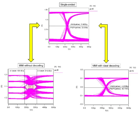
Figure 3.7 presents the data jitter measurements on the Rx-side for single-ended mode
and MMI mode. The operation frequency was 2 GHz. The peak-to-peak jitter for multi-level
signals of MMI was 134 ps, which was much larger than the 33 ps of single-ended mode.
The data jitter of MMI was still larger than that of single-ended mode even after ideal
decoding. This indicates that MMI is more hazardous concerning switching noise than
single-ended mode. Furthermore, the imperfection of decoding will add extra jitter to the
3.3.2 Switching Noise Reduction of Digital Encoder
for Multi-Mode Interconnector
Peak-to-peak data jitter was analyzed for showing the switching noise reduction
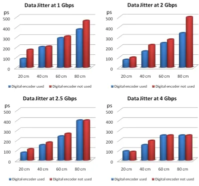
efficiency of a digital encoder. Figure 3.8 shows the reduced data jitter of multi-level signals
at the far-end transmission lines when the digital encoder was used. Time notes represent
peak-to-peak data jitter of multi-level signals. The data jitter was reduced from 215 ps to 157
ps on a 40 cm channel at 2 Gbps. The amount of reduction is not solely from the use of a
proposed encoder since the jitter includes all kinds of noises from the channel. However, it is
clear that the proposed encoder contributes to the reduction of data jitter on MMI mode.
The data jitter reductions were also measured on various length channels at different
frequencies. The graphs in Figure 3.9 show the measurement results of peak-to-peak data
jitter on the channel length from 20 cm to 80 cm at different frequencies.
3.3.3 Signal Integrity Improvement with Pre-emphasis
The performance of a pre-emphasis circuit is typically estimated by an eye-diagram.
The multi-level eye-diagrams were plotted for three cases at the far-end transmission line at
3.5 Gbps before multiplying the decoding matrix: 1) without pre-emphasis, 2) with suitable
pre-emphasis and 3) with over-weighted pre-emphasis. Peak-to-peak data jitters were
compared for all three cases instead of comparing eye-width and height because it is difficult
to define them with a multi-level eye diagram. Figure 3.10 shows the results for all three
cases. It illustrates that appropriate fractional pre-emphasis reduces the data jitter but
over-weighted pre-emphasis causes the ambiguities between levels.
Multi-level eye diagrams include crosstalk noise, so it is hard to conclude the
pre-emphasis efficiency. Hence, the multi-level signals are multiplied by the decoding matrix for
restoring the initial NRZ binary data without crosstalk. The eye diagrams for restored binary
signals are shown in Figure 3.11. It illustrates peak-to-peak jitter and RMS jitter differences
for three different cases. Approximately 50% RMS jitter reduction was achieved by
pre-emphasis.
The overall eye-diagram and data jitter results for each case is graphically
summarized in Figure 3.12.
The numerical data jitter results of restored signals on the Rx-side are summarized in
Table 3-2. The frequency range was from 1 GHz to 3.5 GHz and the channel length was from
20 cm to 40 cm. It illustrates the efficiency of pre-emphasis for reducing the ISI in terms of
data jitter.
3.4 Chip Fabrication and Measurements
3.4.1 Prototype Implementation
The entire circuit had been designed and simulated in 0.13 µm. However, the
proposed design was fabricated in the IBM 0.18 µm process. The layout and test board are
shown in Figure 3.13. In the layout, source voltage and ground for the pre-emphasis part
were separated from the main voltage source and ground to enable and disable the
pre-emphasis function. Four 10 inches, 50 Ω embedded striplines, each with a line width of 5
mils, was manufactured on a FR4 board. The space between lines was scaled as 5 mils.
3.4.2 Measurements
As shown in Figure 3.14(a), the reflection noise and power supply noise reduced the
signal integrity significantly. Figure 3.14(a) shows 1 GHz 5-level signals on the Rx-side.
Data jitters of multi-level signals on the Rx-side for two cases are shown in Figure 3.14(b, c);
Case (b) shows peak-to-peak jitter when the pre-emphasis was disabled, and case (c) shows
the peak-to-peak jitter when the pre-emphasis was enabled. Even though the jitter was
reduced by about 40 ps by enabling the pre-emphasis circuit, the other noises caused
approximately 410 ps of data jitter at 1 Gbps. Supply voltage was 1.8 V. Overall power
consumption was 106.2 mW, and the pre-emphasis portion consumed 27.9 mW at 1 Gbps
operation.
3.4.3 Chip Failure Analysis and Summary
This chapter introduced the new Tx design of MMI for reducing ISI with
pre-emphasis and presented its efficiency with Hspice simulation. However, it was hard to show
the signal integrity improvement from the chip measurement. In the chip fabrication, there
were significant noises which were not expected. The major noise sources were concluded to
be reflection, clock distribution and routing error, and the power and ground noise.
The main reason for reflection was off-chip termination. Off-chip termination has
much more reflection than on-chip termination [27]. However, on-chip termination resistors
were not equipped in this chip. This caused huge waves of multi-level signals and extra data
jitter as shown in Figure 3.14.
An inaccurate clock distribution and routing caused the most of data jitter and slowed
down the operating frequency as shown in Figure 3.14. The pre-emphasis circuit used a total
of 16 clocks and 16 inverse-clocks to generate fractional pulses for controlling pre-emphasis
drivers, and it used 32 flip-flops for making precise one-cycle delays of all digital encoder
outputs to synchronize the inputs of pre-emphasis inputs with the inputs of the main driver.
Therefore, the clock routes for each flip-flop and each pre-emphasis circuit could not
be controlled precisely enough for demonstrating the best performance. In addition, the chip
was fabricated with a different process than the initial circuit design process. The entire
circuit was designed with a 0.13 μm process, but the layout was conducted with a 0.18 μm
process. Insufficient time allowance for the switching process caused poor clock distribution
Finally, the fabricated chip did not include enough decoupling capacitors between the
power supply and ground rails for suppressing the power supply noise. All sub-drivers in this
chip were composed of only NFETs, so the pull-down strength and duty cycle of turning on
and off time for the driver varied significantly if there were large power supply and ground
noises. This also caused the large waves of multi-level signals as shown in Figure 3.14.
Better measurement results are expected by replacing off-chip termination to on-chip
termination, adding sufficient capacitors between the power supply rail to ground rail, and
Chapter 4
Low-Power Advanced MMI
The popularity of portable electrical devices has increased noticeably since the
lap-top computer has been developed. The emergence of the smart phone boosted popularity
dramatically. However, portable and multi-functional devices such as smart phones and
tablet PCs consume much more power than mono-functional devices such as MP3 players
and voice recorders, and they have more interconnects inside of their systems as well.
However, the battery size must be reduced since it is limited by the size of the portable
device. If the portable device must become larger than a back-pack, it will lose its merit as a
portable device, and thus, a low-power interconnect design is preferable for portable
electrical devices.
Unfortunately, the previous MMI design [1] consumed too much power for decoding
since the design did not consider the power efficiency. In this chapter, low-power MMI is
presented, and a more crosstalk-inducing channel is used for presenting the efficiency of
4.1 Channel Model and Coding Coefficients
Two channels were used for the simulations. The first channel was comprised of
embedded four-conductor striplines. The second channel was comprised of double-side
coplanar waveguides without conductor planes on the top and bottom. The modified channels
had identical mutual distances from the center of the channel bundle to each conductor as
well. The dimensions of the transmission line models used for the simulations and their
S-parameter responses are shown in Figure 4.1. Coding coefficients were the same as (3.1) and
(3.2). In a manner similar to Chapter 3, single line-to-ground terminations were used. 42 Ω
and 68 Ω were used for the embedded striplines and double-side coplanar channels,
4.2 Advanced Pre-emphasis for MMI
In Chapter 3, the fractional and multi-level pre-emphasis scheme was proposed for
reducing ISI of MMI without breaking encoding coefficients. However, time synchronization
between pre-emphasis and the main driver suffered due to clock jitter. The entire design was
too sensitive in response to clock synchronization. Each pre-emphasis block required two
negative flip-flops for detecting the difference between a one-cycle delayed bit and a current
bit. It also required 2 clocks and 2 inverted clocks for generating fractional pulses to control a
pre-emphasis sub-driver.
In addition, unnecessary usage of flip-flops wasted extra power to operate flip-flops
and source clock signals. Figure 4.2 represents the entire circuit map for the previously
designed pre-emphasis. For synchronizing pre-emphasis inputs and main driver inputs easily
Digital Encoder x3 x4 u1 x2 x1f(x1...xn) In1 In4 In2 In3 Digital Encoder x3 x4 u1 x2 x1f(x1...xn) Digital Encoder x3 x4 u1 x2 x1f(x1...xn) Digital Encoder x3 x4 u1 x2 x1f(x1...xn) 4 4 4 4 CLK u1 x1 Neg/FF CLK u1 x1 Neg/FF CLK u1 x1 Neg/FF CLK u1 x1 Neg/FF CLK u1 x1 Pos/FF CLK u1 x1 Pos/FF CLK u1 x1 Pos/FF CLK u1 x1 Pos/FF CLK u1 x1 Neg/FF CLK u1 x1 Neg/FF CLK u1 x1 Neg/FF CLK u1 x1 Neg/FF 4GHz 4GHz 4GHz 4GHz 30cm TL
5 Level Driver
TL input T x i n p u ts 4 Driver
Generating code for modal conversion Output patterns
Level 0 Level 1 Level 2 Level 3 Level 4
L L L L H
L L L H H
L L H H H
L H H H H
out4 out3 out2 out1 Pre-em Enabler Coming bits Previous bits Pull up Pull down Transition detector Pre-em Enabler Coming bits Previous bits Pull up Pull down Transition detector Pre-em Enabler Coming bits Previous bits Pull up Pull down Transition detector Pre-em Enabler Coming bits Previous bits Pull up Pull down Transition detector 4 Z Z Z Z a1 1 a2 2 3 a3 4 a4 RX 4 Pre-emphasis 4 4 Pre-emphasis 4 4 Pre-emphasis 4 4 Pre-emphasis
Pull Up pre-emphasis
Pull down pre-emphasis Enable Pull-up TL TL TL TL TL Enable Puu-down TL VDD
Delay constraint 1
Clk to Q delay of flip-flop and Clk to pull up or down pulse delay of pre-emphasis enabler has to be
almost same
Delay constraint 2
Delay from coming bit to PU or PD has be smaller than half clk period
previous current GND VDD clkb clk_delay PU PD Pullup pulse Pulldown pulse ≈80 ps clkb_delay clk clk clk_delay
Pullup pulse: When bit changes 1 to 0 Pulldown pulse: When bit changes 0 to 1
4.2.1 Circuit Architecture
The function of new pre-emphasis is the same as the previous design. However, there
is no clock input. The controller generates pulling-up and pulling-down pulses for
pre-emphasis drivers only with the outputs of digital encoders. It compares delayed data and
current data for detecting the switches. A delay between Data and Delayed Data is generated
by three-stage buffers which have a variable voltage source at the middle stage for
controlling the delay. If the data switches, the controller generates pulses for operating
pre-emphasis drivers in a manner similar to a previous design. Figure 4.3 shows its block
diagram and circuits. This design is solely operated by data inputs. Hence, flip-flops and
clock sources are not needed anymore. The entire circuit was designed with an IBM 0.13 µm
process. Data Delayed Data PUin PDin Data Pre-emphasis Controller ×4
Data Delayed Data Vdd2 GND VDD TL PU4 PU3 PU2
PD2 PD3 PD4 Multi-Level
Pre-emphasis Driver
PU1
PD1