RF CIRCUIT DESIGN INTEGRATED WITH MICROSTRIP DGS
X. Q. Chen, L. H. Weng, Y. C. Guo, andX. W. Shi
National Key Laboratory of Antenna and Microwave Technology Xidian University
Xi’an 710071,P. R. China
Abstract—This paper presents microstrip transmission lines for designing a microstrip open loop resonator bandpass filter and a novel dual band transmitter. Microstrip open loop resonator bandpass filter with the dumbbell DGS under feed lines enhances the harmonic suppressed at the center frequency of 2.44 GHz. An asymmetric dumbbell DGS-integrated microstrip line is applied to the dual band transmitter which performs as a frequency doubler at 6.8 GHz or a power amplifier at 2.4 GHz. For the proposed bandpass filter,it has a wide stopband characteristic with attenuation −25 dB up to 8 GHz and has an −1.25 dB insertion loss by using two dumbbell DGS. Measurements of the dual band transmitter show that in frequency double mode,fundamental suppression and maximum output are
−41 dBc and 7.8 dBm. And in amplifier mode,second harmonic suppression,P1 dB and gain achieve−52.6 dBc,13.7 dBm and 16.5 dB, respectively.
1. INTRODUCTION
which have been developed to suppress the harmonics and realize the compact physical dimensions of RF circuits [4,5].
In this paper,open loop resonator bandpass filter and the dual band transmitter design techniques for wireless LAN transmitter are presented. For the proposed DGS,its equivalent circuit and the stop band characteristics of the microstrip DGS are analyzed and simulated. By changing the dimensions of dumbbell-shape DGS,a improved open loop resonator bandpass filter for WLAN is proposed which provides much larger suppression in the rejection area including the image signal and in-band signal harmonic than the convention one. This filter is characterized with two transmission zeros,low insert loss,and high out-of-band rejection. And the dual band transmitter works as a power amplifier which satisfies the 802.11 b/g frequency band of wireless LAN standard,and it also performs as a frequency doubler with the stop band characteristics of DGS according to the input frequency and bias. Compared with a conventional dual band wireless LAN transmitter,the proposed dual band module operates as an amplifier for the 802.11 b/g signal and as a frequency doubler according to signal frequency which shows well performance in experiment results.
2. RF DEVICES DESIGN WITH DGS
2.1. Bandpass Filter Design
dielectric constant. So,the slow-wave factor increases with inclusion of DGS,which enhances the coupling between lines [12]. As a result, we achieve better passband performance.
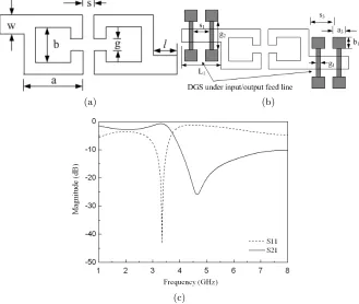
Fig. 1(b) shows the proposed two DGS under both input and output feed lines. The two dumbbell-shape DGS are separated by a distance s1 = 8 mm,and the distance between the second
dumbbell-shape and the loop iss3 = 14 mm. DGS cell consists of two rectangular
slots of length a1 = 6 mm and width b1 = 4 mm which are connected
by a thin transverse rectangular slot of widthg1 = 1.5 mm and length g2= 11.1 mm symmetrically under 50 Ohm microstrip lines with width w= 2.82 mm and length L1 = 30 mm. Fig. 1(c) shows the input and
output DGS transmission lines which behave as a lowpass filter with cut off frequency 3.66 GHz. So they allow the fundamental frequency at 2.44 GHz to pass but attenuate other harmonics at 4.88 GHz and 7.32 GHz.
(a) (b)
(c)
2.2. Dual BandTransmitter Design
In active circuits,harmonic components could be generated from nonlinear semiconductor devices such as Schottky-barrier diodes, varactor diodes,step-recovery diodes (SRDs),and transistors. For active frequency doubler and amplifier,controlling the conduction angle of the signal carrier by the input dc-bias voltage is the main source of harmonic signal generation [13]. As active devices,especially for dual band transmitter the frequency doubler operating at the second harmonic and the power amplifier at the fundamental frequency, the optimum impedances for the maximum powers at both bands and are different. Several factors such as harmonic suppression, impedances matching,bandwidth and insertion loss should be taken into consideration.
Figure 2. The proposed dual band transmitter with DGS block diagram.
The dual band transmitter using microstrip line DGS which works at 2.4 GHz and 6.8 GHz wireless LAN applications is shown in Fig. 2. It consists of a filter,power gain controller (PGC),voltage controlled oscillator (VCO) operating from 2.4 GHz to 3.4 GHz and the amplifier/ frequency doubler module for dual band transmitter. As most conventional dual band transmitter of the wireless LAN system used two separate RF modules for both bands,it requires a power amplifier at each band [13]. Those structures usually require different a voltage controlled oscillator (VCO) for each band. And the VCO should work in very broad bandwidth.
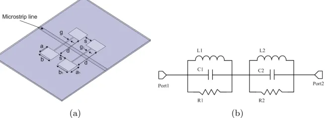
the harmonics suppression and reduce size due to its slow wave effect [16]. Third,its insertion loss is much lower. Extremely small insertion loss values for implementation of RF circuits can be realized. The validity of the modeling method for the proposed DGS unit section and the design method is verified by experiments [17–21]. The DGS applied to a microstrip line causes a resonant character of the structure transmission with a resonant frequency controllable by changing the shape and size of the slot. Figs. 3(a) and (b) show the proposed DGS structure and its equivalent circuit.
(a) (b)
Figure 3. (a) Proposed DGS on the ground plane,(a) Equivalent circuit models of DGS.
In this paper,an asymmetric dumbbell module was proposed. The dimensions of the dumbbell are the following: a= 3.8 mm,b= 5 mm,
s = 4 mm, d = 9 mm, g = 0.3 mm, a1 = 3.9 mm, b1 = 5.2 mm
and g1 = 0.28 mm. The equivalent circuit model with two
LCR-network resonators for the proposed DGS model is shown in Fig. 3(b). The resonant characteristics are modeled by a LC-resonator,and the radiation effect and loss are considered by including resistor,R. Based on the transmission line theory and the spectral domain approach, the equivalent circuit parameters can be expressed using the following equations:
R(ω) = 2Z0
1
|S11(ω)|2 −
2Z0
ωC − 1
ωL
2 −1
(1)
C = ωc
2Z0
ω02−ω2
c
(2)
L = 1
4(πf0)2C
whereZ0 is the 50 Ω characteristic impedance of the transmission line, f0 is the resonant frequency,and ∆f is the −3 dB bandwidth of S21.
The stopband characteristic of DGS with different distance d
which is the length between two rectangular lattices was shown in Fig. 4. Whenddecreases from 10 mm to 8 mm,the attenuation poles move to higher frequency from 3.2 GHz to 3.6 GHz. Usually,the DGS is fabricated to have a wide stopband bandwidth. Here the proposed DGS is designed to achieve the stopband bandwidth which could satisfy the demands of the dual band transmitter from 3.4 GHz to 4.8 GHz.
Figure 4. Comparison of stopband characteristic of DGS with differentd.
The proposed power amplifier works at 2.4 GHz for 802.11 b/g is the other mode of the dual transmitter. The designed dual band circuit based on small signal has been analyzed by large signal with tuning of broadband matching circuits in order to accomplish power gain, linearity and maximum power [20,21]. So when the module operates as the amplifier,the second and third harmonic to the fundamental power at input frequency of 2.4 GHz are suppressed by the stopband characteristics of DGS. The input matching circuit is constructed to transmit the input frequency of 2.4 GHz to 3.4 GHz,and to suppress 3.4 GHz signal which back from output of the amplifier by a LPF structure in Fig. 5. Also output matching circuit is designed to amplify 2.4 GHz and 6.8 GHz output combined with the microstrip DGS.
Figure 5. The proposed power amplifier with matching network.
(a) (b)
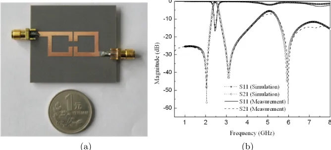
Figure 6. View of convention BPF: (a) Photograph of the fabricated filter,(b) Comparison between the measured and simulated results.
3. RESULTS AND DISCUSSIONS
3.1. Bandpass Filter
The layout of the filter fabricated on a TLX substrate with thickness of 1 mm and dielectric constant of 2.55. The conventional and proposed bandpass filters were simulated with HFSS commercial software and the scattering parameters were experimentally measured using Agilent make Vector network analyzer of model N5230A. We observe the passband center frequency at 2.44 GHz and the 3-dB rejection bandwidth of 200 MHz as shown in Fig. 6. We measure the
and obtained small differences in insertion loss and bandwidth due to fabrication tolerance. It shows higher harmonics centered at 4.88 GHz and 7.32 GHz.
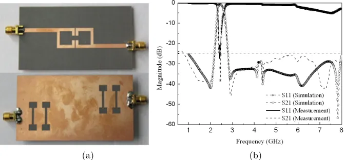
As mentioned above,the photograph of the filter by using DGS under the both feed lines to improve performance is shown in Fig. 7(a). It has been distinctly observed in Fig. 7(b) that the filter has a wide stopband characteristic with attenuation −25 dB up to 8 GHz using two dumbbell-shape DGSs. Due to finite insertion loss of lowpass filter characteristic of DGS transmission lines,the insert loss of the filter is
−1.25 dB which is a little larger than the conventional one.
(a) (b)
Figure 7. Top view and bottom view of BPF: (a) Schematic top and bottom view of BPF,(b) Comparison between the measured and simulated results.
3.2. Dual BandTransmitter
The proposed dual band transmitter was fabricated by using mi-crostrip circuit with HITTITE HMC313 GaAs InGaP Heterojunc-tion broadband MMIC. The substrate parameters are εr = 3.48,and tanδ = 0.002. The photograph of 2.4 GHz and 6.8 GHz transmitter is shown in Fig. 8.
(a) (b)
Figure 8. Photograph of the dualband transmitter (a) Schematic top-view,(b) Schematic ground-view.
Figure 9. Simulated and measured results of the proposed DGS.
loss at 2.4 GHz is about −0.132 dB by simulating while the measured results is about−0.152 dB at 2.4 GHz.
(a) (b)
Figure 10. Measured results (a) Output spectrum measured at 6.8 GHz in frequency doubler mode,(b) Output spectrum measured at 2.4 GHz in power amplifier mode.
4. CONCLUSIONS
This paper demonstrates that a DGS-integrated multifunctional microstrip lines could be successfully used to improve circuit performance in a simple way. The improved the open loop square resonators passband filter with a pair of transmission zeros achieves better bandwidth and low insertion loss. Two pairs of DGS structures are etched under input and output feed line. The proposed filter with DGS has an −1.25 dB insertion loss and which affects very little on passband performances and reduces the spurious frequencies successfully with attenuation −25 dB up to 8 GHz. The measured results agree well with the EM simulated results. These DGS-loaded microstrip lines were applied into designing a dual band transmitter and bandpass filter. By the stopband characteristics of proposed DGS from 3.4 GHz to 4.8 GHz,the second harmonic of the amplifier and fundamental power of the frequency doubler were suppressed. the P1 dB and gain achieve 13.7 dBm and 16.5 dB,respectively. In the frequency double mode,fundamental suppression and maximum output are−41 dBc and 7.8 dBm at 6.8 GHz. The implementation and performance measurement shows that the proposed DGS will be useful in the development of microstrip circuit design.
ACKNOWLEDGMENT
REFERENCES
1. Jeon,J. H.,J. H. Choi,S. M. Kang,T. Y. Kim,W. Choi,and K. H. Koo,“A novel dual band transmitter for WLAN 802.11 a/g applications,” IEEE MTT S Int. Microwave Symp. Dig.,Vol. 2, 1285–1288,2004.
2. Zhang,P.,L. Der,D. Guo,I. Sever,T. Bourdi,C. Lam, A. Zolfaghari,J. Chen,D. Gambetta,B. Cheng,S. Gowder, S. Hart,L. Huynh,T. Nguyen,and B. Razavi,“A single-chip dual-band direct-conversion IEEE 802.11 a/b/g WLAN transceiver in 0.18-µm CMOS,” IEEE J Solid State Circuits,Vol. 40,No. 8, 1932–1937,2005.
3. Chang,C.-F. and S.-J. Chung,“Bandpass filter of serial configuration with two finite transmission zeros using LTCC technology,”IEEE Trans. Microwave Theory Tech.,Vol. 53,No. 7, 2383–2388,2005.
4. Chung,Y.,S.-S. Jeon,S. Kim,D. Ahn,J.-I. Choi,and T. Itoh, “Multifunctional microstrip transmission lines integrated with defected ground structure for RF front-end application,” IEEE
Trans. Microwave Theory Tech,Vol. 52,No. 5,1425–1432,2004.
5. Xiao,J.-K.,S.-W. Ma,S. Zhang,and Y. Li,“Novel compact split ring stepped-impedance resonators (SIR) bandpass filters with transmission zero,”J. of Electromagnetic Waves and Applications, Vol. 21,No. 3,329–339,2007.
6. Zhang,J. and X.-W. Sun,“Harmonic suppression of branch-line and rat-race coupler using complementary spilt ring resonators (CSRR) cell,” Progress In Electromagnetics Research Letters, Vol. 2,73–79,2008.
7. Fan,J.-W.,C.-H. Liang,and Y.-J. Wu,“Compact dual-band and tri-band filters with loaded open-loop resonators,”Journal of
Electromagnetic Waves and Applications,Vol. 21,No. 15,2371–
2378,2007.
8. Parui,S. K. and S. Das,“Performance enhancement of microstrip open loop resonator band pass filter by defected ground structures,” Conf. Proc. IEEE Int. Workshop Antenna Technol.
Small Smart Antennas Metamater. Applic.,483–486,2007.
9. Zhang,F. J. W. and J. S. Zhang,“Wideband cavity-backed patch antenna for pcs/imt2000/2.4 GHz WLAN,” Progress In
Electromagnatics Research,PIER 74,39–46,2007.
137–148,2007.
11. Chen,X. Q.,X. W. S.,Y. C. Guo,et al.,“A novel dual band transmitter using microstrip defected ground structure,”Progress
In Electromagnatics Research,PIER 83,1–11,2008.
12. Hong,J.-S. and M. J. Lancaster,“Theory and experiment of novel microstrip slow-wave open-loop resonator filters,” IEEE Trans Microwave Theory Tech.,Vol. 45,No. 12,Part 2,2358–2365,1997. 13. Park,Y.,R. Melville,R. C. Frye,M. Chen,and J. S. Kenney,
“Dual-band transmitters using digitally predistorted frequency multipliers for software defined radios,” IEEE MTT S Int.
Microwave Symp. Dig.,Vol. 2,547–550,2004.
14. Xiao,J.-K.,“Novel microstrip dual-mode bandpass filter using isoscelles triangular patch resonator with fractal-shaped structure,” Journal of Electromagnetic Waves and Applications, Vol. 21,No. 10,1341–1351,2007.
15. El-Tokhy,M. A. and H. K. Mansour,“A 2.3-MW 16.7-MHz analog matched filter circuit for DS-CDMA wireless applications,” Progress In Electromagnetics Research B,Vol. 5,253–264,2008. 16. Choi,H.-J.,J.-S. Lim,and Y.-C. Jeong,“A new design of Doherty
amplifiers using defected ground structure,” IEEE Microwave Compon. Lett.,Vol. 16,687–689,2006.
17. Zainud-Deen,S. H.,M. E. S. Badr,E. El-Deen,K. H. Awadalla, and H. A. Sharshar,“Microstrip antenna with defected ground plane structure as a sensor for landmines detection,”Progress In Electromagnatics Research B,Vol. 4,27–39,2008.
18. Naghshvarian-Jahromi,M. and M. Tayarani,“Miniature planar uwb bandpass filters with circular slots in ground,” Progress In Electromagnatics Research Letters,Vol. 3,87–93,2008.
19. Oskouei,H. D.,K. Forooraghi,and M. Hakkak,“Guided and leaky wave characteristics of periodic defected ground structures,” Progress In Electromagnatics Research,PIER 73,15–27,2007. 20. Park,Y.,R. Melville,R. C. Frye,M. Chen,nad J. S. Kenney,
“Dual-band transmitters using digitally predistorted frequency multipliers for reconfigurable radios,” IEEE Trans. Microwave Theory Tech.,Vol. 53,115–122,2005.
21. Choi,H.-J.,J.-S. Lim,and Y.-C. Jeong,“A new design of Doherty amplifiers using defected ground structure,” IEEE Microwave