IJEDR1402258
International Journal of Engineering Development and Research (www.ijedr.org)2908
Studying impact of transistor aging and process
parameter variation on the performance of analog
circuits
1
Hemant Madan Khadilkar
1Bangalore, India
________________________________________________________________________________________________________
Abstract— NBTI and HCI emerged as a major reliability concern for deep-submicron CMOS technology. For 65nm technology, process parameter variation is also creating problems for reliable design. We report simulation study for NBTI mechanism for PMOS and HCI for NMOS. Comparator circuit is used to study the impact of NBTI on offset voltage. The process parameter variation is also studied. Offset voltage is modeled in terms of process parameters and effect and sensitivity for these process parameters has been studied.
Index Terms— NBTI, reliability, process parameter variation, Design of Experiment (DOE)
________________________________________________________________________________________________________
I.INTRODUCTION
Aggressive scaling of CMOS process technology has introduced serious challenges on the lifetime reliability of Integrated Circuits (IC‘s). The reliability of integrated circuits has thus become a focus of concern due to extreme scaling of device sizes. The degradation of transistors based on their working time, also called aging, causes significant changes in certain device characteristics that has adverse effects on the performance of critical circuit parameters. Transistor aging reduces the reliability of digital and analog circuits [1], [2]. Reliability degradation in MOSFET‘s can be due to different physical mechanisms like Negative Bias Temperature Instability (NBTI), Hot Carrier Degradation (HCI). Process variability is another issue in deep sub-micron CMOS technology which has a significant impact on the performance of the devices. Process variability causes device parameters to change randomly, producing statistical spread on circuit performance parameters. This leads to smaller circuit yield after the production. Transistors having feature size of 65nm and smaller are impacted by process related variations of threshold voltage, oxide thickness, mobility and other process related parameters. Process variation exists for fresh devices, but becomes worse for aged ones. Due to increasing electric fields and high power dissipation in IC‘s (leading to increased working temperature of devices) in sub-nanometer CMOS technologies, integrated circuits become more and more susceptible to transistor aging effects. Recent studies show that the aging of transistors is not just a function of bias voltages but it also has a strong dependence on temperature, as well as process parameters of individual devices [3]. The transistor degradation effects (NBTI and HCI) causes a shift of transistor parameters (example: threshold voltage for NBTI and threshold voltage and mobility for HCI), possibly causing circuit malfunction. Combined with process variability, the yield of an IC can therefore reduce significantly within its lifetime.
The focus of this paper is to study the impact of aging and process variability on the performance of analog circuits. For aging, only the Negative Bias Temperature Instability mechanism is considered. The simulation is done with the ELDO simulator. The impact of aging and process variation for different temperatures has also been included. This paper is organized as follows: Section II explains aging mechanisms (NBTI and HCI) theoretically. Section III demonstrates the aging and process variability effect on the comparator circuit. Finally conclusion is given in section IV.
Abbreviations and Acronyms
NBTI: Negative Bias Temperature Instability HCI: Hot Carrier Injection
CMOS: Complementary Metal-Oxide-Semiconductor
PMOS/NMOS: Positive channel/Negative channel Metal-Oxide-Semiconductor IC: Integrated Circuits
MOSFET: Metal-Oxide-Semiconductor Field Effect Transistor VTH: Threshold Voltage
ID: Drain Current
ADC: Analog-Digital Converter DOE: Design of Experiment RMSE: Root Mean Square Error
IJEDR1402258
International Journal of Engineering Development and Research (www.ijedr.org)2909
II.AGING MECHANISMThe electrical operation of a chip may lead to degradation of its performance over time. The Negative Bias Temperature Instability and Hot Carrier effects have raised concerns in deep-submicron CMOS technology and have to be considered at design time. The devices on a chip will have different degradation rates and levels during chip‘s lifetime depending on their individual operating conditions. An accurate modeling of aging degradation needs analysis of each device‘s usage in a circuit in order to study the sensitivity to the aging effects. After we have this degraded data over certain lifetime period, it is then possible to run the simulations with degraded data to check if the circuit performances are met with the designed values. The important point to note here is that the impact of aging on performances varies greatly with each circuit. The reliability of integrated circuits is calculated from degradation of certain electrical characteristics of transistor based on time. Transistor aging accelerates with scaling because of the increased electric fields. The objective of aging and reliability simulation is to be able to model the gradual damage, which occurs to the devices in a certain design, causing degradation in the performance of that design. It is required to evaluate the amount of degradation occurring in a certain period of operation and examine the circuit performance after this period. The modeled damage could follow one or more several damage mechanisms, which show gradual degradation in device performance. The amount of damage each transistor suffers depends on bias conditions applied on specific transistor and the time duration through which this bias was applied. Hence it is important to study the impact of aging on each transistor in a circuit and find out the critical devices for the circuit performance and circuit reliability. Once these critical devices are recognized, further steps can be taken in circuit design to reduce the effect of aging on the circuit. In this section two aging mechanism namely NBTI and HCI are explained theoretically.
Negative Bias Temperature Instability (NBTI)
Negative Bias Temperature Instability (NBTI) is one of the most critical reliability issues in deep-submicron CMOS technology. It occurs at high temperature (around 800C to 1500C) under high gate voltage (VGS=-VDD) and affects mostly p-channel MOSFET‘s. It is ascribed to breaking of Si-H bonds which are formed during passivation process at the interface of bulk (Silicon) – oxide (Silicon-dioxide) interface. The bonds break when subjected to large negative gate bias for long time. This effect gets worse at high temperatures [4],[5]. Interface trap creation is not the only reason behind the degradation but hole trapping also occurs. Hole trapping is the main reason why NBTI has recovery effect, which makes accurate measurement of degradation difficult [6]. NBTI causes increase in absolute value of threshold voltage, degradation of mobility, drain current and trans-conductance of PMOS. The aspects found to lead to increasing susceptibility to NBTI are- 1) Higher oxide electric fields due to oxide scaling, 2) Higher temperatures due to higher power dissipation, 3) Incorporation of Nitrogen. Figure 1(a) shows the degradation of VTH for PMOS due to NBTI as a function of temperature. It can be seen that the degradation increases as the temperature increases. Fig. 1(on Right) shows the % degradation of VTH for PMOS due to NBTI for different corner processes.
Hot Carrier Degradation (HCI)
Hot carrier degradation is another important degradation mechanism for MOSFET‘s. Major source of the hot carriers is the electric field inside the channel of the transistor. The energetic carriers or the carriers generated during impact ionization can produce parametric degradation. This means shift in device characteristics. Hot carrier degradation occur when there is high Drain-Source voltage (VDS) and optimum Gate-Source voltage (VGS). In deep saturation region of MOS transistor, applied Drain-Source voltage drops linearly across the channel, starting from the Drain-Source end till the pinch-off point. The remaining VDS drop across small pinch-off region. This creates a spike in lateral electric field in this region. When the carriers pass through this region, they get more energy than that can be dissipated in the crystal lattice structure through non-destructive energy transfer. These carriers are not in thermal equilibrium with the surrounding and are ‗hotter‘. This additional energy possessed by these hot carriers can cause bond breakage at bulk-oxide interface through impact ionization. This damage starts at the Drain end and slowly progresses towards the Source end with the time. These carriers can be injected into the gate dielectric, where they can be trapped or can induce interface traps. This might lead to threshold voltage shift, degradation of Drain current. Hot carrier Degradation is found to have a relation with the gate length as against found in NBTI. HCI degradation can be reduced by increasing channel length. HCI is found to have significant impact on NMOS as against PMOS. It is because of the fact that the mobility of electrons is about three times to that of holes because of which electrons gets hotter than holes. Higher Drain current degrades HCI reliability since it generates more carriers by impact ionization.
Fig.1 shows VTH degradation for PMOS due to NBTI as a function of temperature. It can be seen that the effect of NBTI gets worse with increase in temperature. Fig. 2 shows the degradation of ID and VTH for NMOS with HCI, simulated with ELDO at T=270C for two different Gate-Source Voltages. As explained in earlier part that HCI occurs for VDS=VDD and for optimal values of VGS. As VGS value is varied from 0.6 Volts to 0.9 Volts, an eventual increase in Drain current (ID) accelerates HCI degradation. That means for higher value of ID, degradation in both VTH and ID is higher.
III.SIMULATION RESULTS
A dynamic comparator is chosen as a test structure to study the effect of aging and process parameter variation. Comparator is one of the main building blocks of an ADC. Dynamic latched comparators have gained importance because of their high power efficiency. The general design considerations of the comparator are offset, noise and meta-stability. There are mainly two types of offset voltages in comparator: 1) offset voltages from the mismatch in transistor threshold voltages due to process variation, 2) offset voltages from the mismatch in parasitic capacitors.
IJEDR1402258
International Journal of Engineering Development and Research (www.ijedr.org)2910
Figure 1: VTH degradation for PMOS due to NBTI as a function of temperature (Left), VTH (%) degradation for PMOS due toNBTI for different corner processes (Right)
Figure 2: VTH (%) degradation for NMOS with HCI (Left), ID (%) degradation for NMOS with HCI (Right), both simulated with ELDO at T=270C
IJEDR1402258
International Journal of Engineering Development and Research (www.ijedr.org)2911
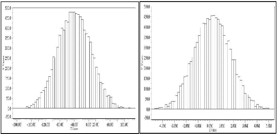
Figure 4: Offset spread for fresh and aged circuit with process variationasymmetrical comparator circuit. NBTI is chosen to be the main aging mechanism. The simulations are done with ELDO at 800C and 1500C. The degradation of each PMOS transistor in a circuit is noted (See Table 1) and critical transistors are recognized for circuit performance parameters. It is seen that transistor pair M7-M8 are critical as against the pair M9-M10. The degradation levels of VTH are same for M9-M10 but for M7-M8 pair, the degradation level for VTH is different. The relative degradation of M7-M8 pair is the main reason behind the variation in offset of comparator for the aged circuit. Table 1 shows the input offset and measured offset and degradation of M7, M8, M9 and M10 transistors for T=800C and T=1500C.
Table 1: Input and measured offset voltages for comparator circuit along with NBTI degradation for transistors at T=800C and T=1500C
Input Offset
Measured Offset (Age=20 yrs)
Error in Offset
Degradation in VTH for Different Transistors
Relative VTH Shift for pair M7-M8
M7 M8 M9 M10
0 0.8333mV 0.8333mV 0.2mV 3.6mV 7.1mV 7.1mV 3.4mV
T=800C
10mV -8.958mV 1.042mV 0.2mV 4.5mV 7.1mV 7.1mV 4.3mV
-10mV 9.7778mV 0.2222mV 4.1mV 3.6mV 7.1mV 7.1mV 0.5mV
0 1.4421mV 1.4421mV 0.1mV 5.2mV 10.2mV 10.2mV 5.1mV
T=1500C
10mV -8.191mV 1.8091mV 0.1mV 6.5mV 10.2mV 10.2mV 6.4mV
-10mV 9.701mV 0.2987mV 5.9mV 5.2mV 10.2mV 10.2mV 0.7mV
It can be seen that the polarity of asymmetry introduced has a significant effect on degradation of VTH for M7-M8 pair and eventually on the offset error. To study the effect of process parameter variation, we consider the comparator circuit without any asymmetry. In such a condition, offset voltage shows some error because of aging as can be seen from Table 1. In process variation analysis, we intend to know how much this offset (Fresh and Aged) varies because of process parameter variation. Only global variations are considered for this study. In order to limit the number of parameters to be declared for each device, some global parameters have been grouped together according to the main device performance. Here psvtlp and nsvtlp are used as one parameter for specific variations of (Standard VT Low Power) SVTLP PMOS and NMOS respectively. The specific number of sigma impacts the variations of VTH, mobility, access resistance, junction capacitance for all devices used in the circuit. Pre-analysis is done first in order to detect important global parameters, which affects the selected circuit performance. This helps to reduce the number of simulations during analysis step. Next Design of Experiment (DOE) is done with these selected important parameters. The selected circuit performance is expressed in terms of process parameters with a linear polynomial equation. Both fresh and aged offset polynomials are given by equations 1 and 2. The circuit performance model is defined as an analytical polynomial expression of the parameters. The polynomial expression can be linear or quadratic, with and without interactions.
Offset(Fresh)=A0+A1*poly_cd+A2*active_cd+A3*lp_dtox+A4*nsvtlp+A5*psvtlp (1) Offset(Aged)=A0+A1*poly_cd+A2*active_cd+A3*lp_dtox+A4*nsvtlp+A5*psvtlp (2)
IJEDR1402258
International Journal of Engineering Development and Research (www.ijedr.org)2912
traditional normalized spread of simulated (YS) and measured (YM evaluated using polynomial expression) circuit performance values at all scenarios of the DOE.R-squared = 1- SUM ((YM-YS) (YM-YS)) / SUM ((YM-Ŷ) (YM- Ŷ))
where Ŷ is the mean of simulated circuit performance model. Expressed as a percentage, regression coefficient statistic indicates that the performance model fitted explains a certain rate of variability of the circuit performance.
Table 2: Important process parameters affecting offset (Fresh and Aged) along with their respective sensitivities Fresh (Sensitivity) Aged (Sensitivity)
A0 2.84825e-6 8.19905e-4
A1 -9.49417e-7 (20%) -1.76583e-6 (0%)
A2 (active_cd) -9.49417e-7 (20%) -6.9675e-4 (46.51%) A3 (lp_dtox) -9.49417e-7 (20%) 7.46258e-4 (53.36%)
A4 9.49417e-7 (20%) 3.29617e-5 (0.1%)
A5 -9.49417e-7 (20%) 1.61408e-5 (0.02%)
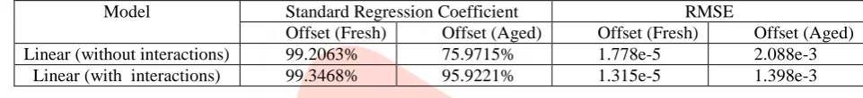
Table 3 below shows the standard regression coefficient and Root Mean Square Error for linear model (with and without interaction between process parameters) for fresh and aged offset.
Table 3: Standard Regression Coefficient and RMSE for Linear model (with and without interactions between process parameters) for fresh and aged offset
Model Standard Regression Coefficient RMSE
Offset (Fresh) Offset (Aged) Offset (Fresh) Offset (Aged)
Linear (without interactions) 99.2063% 75.9715% 1.778e-5 2.088e-3
Linear (with interactions) 99.3468% 95.9221% 1.315e-5 1.398e-3
IV.CONCLUSION
In this work, we have talked about the theoretical explanation behind NBTI and HCI mechanisms. Next, the impact of NBTI and HCI on PMOS and NMOS transistors has been studied. It can be seen that NBTI degradation increases with temperature while HCI degradation becomes worse for higher Drain currents. Comparator offset shows some variations with NBTI aging. The offset voltage has been modeled with linear polynomial expression showing the impact and sensitivity of different process parameters for both fresh and aged circuit. Finally the standard regression coefficient and RMSE for linear model is calculated.
V.ACKNOWLEDGMENT
I would like to thank Professor Lirida Naviner and Professor Herve Petit (Telecom ParisTech) for giving me the opportunity to work with them and guiding me throughout my tenure in Telecom ParisTech. I would also like to thank all my co-researchers in Telecom ParisTech for motivating me during the difficult times. Finally, I would like to thank my parents, my sisters and my lovely wife Supriya for motivating and being with me through the difficult times.
REFERENCES
[1] W. Wang, S. Yang, S. Bhardwaj, S .Vrudhula, F .Liu and Y. Cao. ―The Impact of NBTI Effect on Combinational Circuit: Modeling, Simulation, and Analysis‖, IEEE transactions on very large scale integration (VLSI) systems, Vol. 18, number 2, February 2010.
[2] L. L. Lewyn, ―Physical Design and Reliability Issues in Nanoscale Analog CMOS Technologies‖, NORCHIP 2009, pages 1-10.
[3] D. K. Schroder, ―Negative bias temperature instability: What do we understand?‖, Microelectronics Reliability 47 (2007), pages 841-852.
[4] H. Kufluouglu and M. A. Alam, ―Theory of Interface-Trap-Induced NBTI Degradation for Reduced Cross Section MOSFET‘s‖, IEEE transactions on electron devices, volume 53, number 5, May 2006.\
[5] G. Cellere, M. G. Valentini and A. Paccagnella, ―Effect of channel width, length, and latent damage on NBTI‖, IEEE International Conference on Integrated Circuit Design and Technology,2004.