Modelling and Evaluation of Electrical Resonance Eddy Current
for Submillimeter Defect Detection
Yew L. Hor1, *, Vinod K. Sivaraja2, Yu Zhong1, Bui V. Phuong1, and Christopher Lane2
Abstract—Eddy current (EC) inspection is used extensively in non-destructive testing (NDT) to detect surface-breaking defects of engineering components. However, the sensitivity of conventional eddy current inspection has plateaued in recent years. The ability to detect submillimetre defects before it becomes critical would allow engineering components to remain in-service safely for longer. Typically, it is required that higher frequency EC is employed to achieve a suitable sensitivity for detection of such submillimetre defects. However, that would lead to significant electromagnetic noise affecting the sensitivity of the inspection. To overcome this issue, the electrical-resonance based eddy current method has been proposed, where the electrical enhanced resonance signal increases the contrast between signal and noise, thus improving the sensitivity of the defect detection. This work aims to investigate the electrical-resonance system via simulation technology using combination of fast numerical-based simulation and circuit approach. Leveraging on this model, the detection system can be optimized by performing parameters tuning. Investigation of both experiment and simulation develops a precise calibration model for submillimeter defects detection.
1. INTRODUCTION
Many NDT methods have been developed for structural health monitoring in various industry verticals such as aerospace, construction, oil & gas, transportation, and power plant. Among all, eddy current method is a well developed method implying induced current to detect breaking surface due to its low cost and simple equipment setup. However, the inspection sensitivity of conventional eddy current inspection has deteriorated over small submillimeter (sub-mm) defects [1–4]. Typically, such sub-mm defects often require higher frequency in order to achieve sufficient sensitivity as shallow skin-depth creates stronger interaction between the eddy current and defect [5]. For example, submillimetre defect inspection of aerospace material such as titanium alloy, Ti6Al-4V, would ideally be operated between 5 and 10 MHz. However, using such a high frequency, the detection system would suffer from higher electromagnetic noise [6]. It should be noted that using probe operating at low frequency is limited to larger defect size and shape [7, 8]. Besides making use of advanced signal/image processing techniques to improve the signal-to-noise ratio (SNR) for small cracks, there are techniques developed to further enhance the limitation in detection capability of conventional eddy current inspections such as pulsed eddy current (PEC) [9–11] and near electrical resonance signal enhancement (NERSE) [12, 13]. In this technique, the eddy current probe is driven by current source sweeping through multiple frequencies close to its electrical resonance peak, where the response signals can be significantly boosted above the threshold of (electrical) background noise, thus enhance the resolution of the detected defect. It has been seen that the optimization process of EC probe is usually needed in order to attain best performance for the inspection system, but it is time consuming and costly to conduct such process through practical
Received 29 October 2018, Accepted 11 December 2018, Scheduled 27 December 2018
* Corresponding author: Yew Li Hor ([email protected]).
1 Institute of High Performance Computing, 1 Fusionopolis Way, 16-16 Connexis, Singapore 138632, Singapore. 2 Advanced
trials. Hence, there is an opportunity to use high-fidelity computer models to simulate eddy current inspections for optimizing equipment design, testing parameters and signal processing to further enhance the detection sensitivity. On the other hand, in order to properly conduct the inspection as well as for an adequate interpretation of the results, certain parameters and physical process must be well defined and understood. This may vary from one case to another, and mostly depend on the structure of the material and characteristic associated with the defects being analyzed. Numerical simulation is an appropriate tool for studying different phenomena that take place during an inspection, thus aiding in the efficiency evaluation of the inspection method and the optimization of the inspection equipment.
However, there is still a challenge to have an efficient model that would be able to quickly and accurately simulate the response of eddy current probe to submillimeter crack in alloy, which is well known for its microstructural background noise due to different crystallographic orientations of the grains. One reason behind the limitation in detection sensitivity is the lack of high-fidelity computer models available to simulate eddy current inspections, and the optimization process has to be performed through practical trials, which are costly and highly time consuming. Many eddy current models employing electromagnetic modeling techniques, such as Finite Element Method (FEM) or Integral Equation (IE), have been developed over the years for emulating NDT inspections [14–16]. In addition, there is growing interest in adopting model-based inversion technique for quantifying the depth information of cracks, making fast and efficient eddy current models more and more attractive [17, 18].
In this paper, attempt has been made to develop a fast model to simulate the response of eddy current probes to detect small cracks (especially closed fatigue crack with bridge connection) in multi-layered conducting structure, with the ultimate aim for its application in inversion-based NDT. The contribution of this work is in the development of a more stable IE-based model to evaluate the impedance variation due to cracks within the layered structure, and to provide a flexible interface for coupling with circuit analysis to perform the NERSE simulation to accurately emulate the electrical resonance detection system. The obtained simulated result is in good agreement with experimental data.
2. MODELING METHODOLOGY 2.1. Electromagnetic Modeling
The electromagnetic (EM) model of ferrite-core current coil above a layered electrically conducting structure has been developed to simulate the response of eddy current due to the existence of cracks within the structure [19]. The impedance variation due to crack within such conductive media can be calculated by the reciprocal theorem, as:
ΔZ =−1 I
coil
Δ ¯E(¯r)·J¯(¯r)dr¯=−1 I
crack
¯
Einc(¯r)·J¯ind(¯r)d¯r, (1)
where ¯E is the total electric field; ¯J is the current density of the coil withI the current carrying on each turn of the coil; ¯Einc is the incident electric fields on the crack from the coil and ferrite; and ¯Jind is the
induced electric current on the crack due to the change of the material within the conductive media [6]. Equation (1) can be solved using integral equation, where the computational complexity and the stability of the algorithm are mainly addressed in the computation of the incident fields that involves the solution of the integral Equation (2) describing the field behavior within ferrite structure:
¯
H(¯r) = ¯Hinc(¯r) + (−iω0)
D ¯ ¯
Gr,¯ r¯M¯ r¯dr¯, (2)
where ¯G¯(¯r,r¯) is the dyadic Green’s function for the background layered media [20, 21]; D is the ferrite domain; ¯r and ¯r are the computation points within D; ¯H is the magnetic field; ¯Hinc is
the incident magnetic fields from direct incidence from the coil and reflected incidences from the layered media; M¯ is the induced magnetic sources within the ferrite structure; 0 and μ0 are the
permittivity and permeability, respectively. The relation between the magnetization and magnetic field ¯
(MoM) with Galerkin’s scheme to find ¯M, with which the total incident electric fields from the coil and ferrite structure within the conductive layered media can be obtained. The calculation can be further accelerated to address the issue of a fully dense matrix due to the interactions between the induced secondary magnetic sources within the ferrite structure based on the fast multipole method, which could drastically reduce the costs from O(N2) to O(NlogN) where N is the matrix size. In the proposed model, the reflected waves from the layered media were constructed by using the phase matching scheme in the boundary conditions, accomplished by an iterative solver such as conjugate gradient method result in a stable solution.
2.2. EM Circuit Co-Simulation-Based EREC
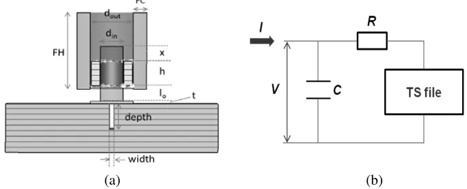
The behavior of the coil sensor structure is accurately described using full-wave simulation, in which the full range of Maxwell’s equation is solved for all effects without approximations. Enhanced response of eddy current signal via resonance can be achieved by incorporating the EM model into an equivalent lumped electric circuit, which can be solved in SPICE-like circuit simulators to perform the system-level simulation of the eddy current NDT system [22, 23]. Here, the equivalent circuit of the 3D EM structure is a 1-port network with its parameter represented by the impedance found by solving the EM problem in the previous part. This can be imported to the circuit simulator via an ASCII text file. The effect of the coaxial cable, which connects the current source to the eddy current probe, was taken into account by its characteristic capacitance C. The equivalent circuit model is shown in Fig. 1, and the Touchstone (TS) file (Fig. 2(b)) accounts for the response of EM model; and the resistance R is the internal resistance value of the coil.
When the sensor is placed in free space, it can be simply demonstrated as a parallel inductor-capacitor circuit model as shown in Fig. 1(a). The resonance frequency in free space is ω0 = πf0 =
1/√L0C0. When the coil is brought closely to electrically conducting material, the equivalent circuit
(a) (b)
Figure 1. Equivalent circuit model of the sensing system (a) when the probe is on free space, (b) when the probe is on top of a conductive material.
(a) (b)
is extended to the coupling model forming a transformer circuit diagram as shown in Fig. 1(b). The coupling model consists of passive series inductor and resistance with coupling coefficient expressed as
k2= 2
1−(ω0/
ω)2
(3)
where ω0 is the resonance frequency in free space, and ω is the resonance frequency due to coupling
effect. The resonance frequency is simplified as
ω = 1
C0L0
1−k2+k4
4 (4)
The impedance of the circuit model in free space is expressed by Kirchhoff’s law as
Z1= R1
+jωL1
1 + jωR1C−ω2L1C
(5)
And the impedance for the coupling model is expressed as
Z2=R1+jωL1
1−k2+ ωL1R2k
2
R2−ω2L22
(ωL2−jR2) (6)
2.3. Modeling and Simulation of EREC System
The modelling of the detecting system was performed using 3D electromagnetic simulation with integration of the circuit co-simulator. Fig. 2(a) shows the diagram of the eddy current probe. The probe was driven by a current source of 50 mA and placed on top of the testing material. The simulation is performed by sweeping frequency from 1 MHz to 6 MHz, with detailed probe parameters and detection system listed in Table 1. To emulate the inspection conditions, a layer of Teflon tapes is placed in between the coil and conductive material. The thickness of Teflon (t) layer is corresponding to the lift-off of the probe, which is approximately 0.08 mm. The capacitance of 184.8 pF contributed from coaxial cable that connected to the probe and oscilloscope was included in circuit simulation. And the effective resistance of the system used in our simulation is 25 ohms. This value was used to model the system level performance of the device. The equivalent circuit model of the system used in circuit co-simulation is simplified as in Fig. 2(b), where the touchstone file comprises the information obtain from 3D EM simulation, which is the obtained impedance profile versus increasing frequencies.
Table 1. Probe and system specifications.
Parameters (unit) Value Coil:
inner diameter,din (mm) 0.972 outer diameter,dout (mm) 1.592
height, h (mm) 1.006
liftoff,t(mm) 0.08
number of turns 64
Ferrite:
Height,FH 4.26
wall thickness,FC 0.551 core-length, x+h+lo (mm) 1.675
3. EXPERIMENTAL SETUP OF EREC DETECTION SYSTEM
(a) (b)
Figure 3. (a) Schematic diagram of data collection system and (b) CT scan image of the probe and its measured parameters in unit of millimeter.
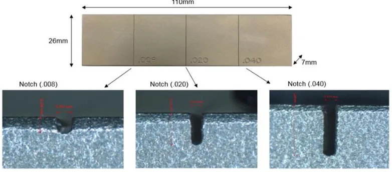
Figure 4. Images of Ti-6Al-4V calibration block notches.
the eddy current probe via the current source which converts the input voltage into a drive current and enables the input and output voltages across the probe to be measured. The current source is connected to the digital oscilloscope that displays the input signal and the eddy current response data received from the probe. The CT scanning image of the eddy current probe is shown in Fig. 3(b). The trigger output from function generator is connected to the oscilloscope to synchronize the data collection. The systems is controlled from a laptop using LabView software to automate the data collection process. The tested specimen is placed on the X-Y stage which is manipulated via the laptop connected to the stage controller. The probe holder houses the EC single coil probe in position while the test specimen moves under it in a raster scan motion.
We used the probe to detect the notches in various depths varying from 0.2 to 1 mm. The specimen tested here is a Titanium alloy (Ti-6Al-4V or Ti 6-4) calibration piece, which measures approximately 110 mm(L)×26 mm(W)×7 mm(H) in size with conductivity of 5.8×10⁵Sm−1. The width, depth and profile details of the respective notches are listed in Fig. 4 and Table 2, respectively.
4. RESULTS VALIDATION
Table 2. Data measured from TI 6AL4V calibration block.
Specifications Notch (0.008) Notch (0.020) Notch (0.040)
Width (mm) 0.181 0.175 0.173
Depth (mm) 0.206 0.522 1.034
Average RA (3 points) 0.598µm
Measured Conductivity 5.8001×10⁵ [S/m]
with the presence of defects on the inspection surface, which is caused by the reduction in the coupling coefficient from that of the eddy current system coupled to an undamaged surface. This will result in a shift in the resonant frequency of the response signal.
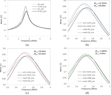
Figure 5(a) shows the comparison results of both experimental testing and simulation with and without the present of the structure under test. The resonance frequencies of air are 2.670 MHz and 2.657 MHz, while the resonance frequencies of Ti-6Al-4V are 2.727 MHz and 2.707 MHz for simulation and experiment, respectively. The results agree with each other with the percentage of error less than 0.7%. It should be noted that the resistance only causes the change of amplitude of the resonance and
(c) (d) (a) (b)
has no effect on the shifting frequency. Hence, the detection mechanism remains valid as long as the signal is boosted above the noise level.
Figures 5(b)–(d) show the notch testing results for both measurement and simulation that show a good agreement. The frequencies shifting in simulation result are 0.0295 MHz, 0.0225 MHz and 0.014 MHz for notch 04, notch 02 and notch 008, respectively, compared to the experimental result: 0.01232 MHz for notch 04, 0.0105 MHz for notch 02, and 0.00168 MHz for notch 008. The large percentage of error encounter from experiment and simulation result especially from result of notch 008 is due to several reasons. The electrical resonance frequency of the sensor can be affected by various factors including circuit components capacitance and resistance of the cable connector, liftoff, and tilt of the probe when performing the scanning. They will affect the accuracy of experiment result, while in simulation, the error could be reduced if smaller frequency step size is used. It should be noted that the electrical resonance frequency of the sensor can also be affected by other factors such as temperature and degree of surface roughness, which currently could not be taken into consideration in our simulation model.
5. STUDY OF PROBE PARAMETERS
Operating at frequency close to resonance leads to a greater sensitivity since the noise issue is eliminated. In order to enhance the resolution in submillimeter detection, we had performed optimization for the probe in various parameters studies includes coil and core parameters as well as the capacitance from the cable that connects to the probe. Fig. 6(a) shows the impedance enhanced and resonance shifting with changing of capacitance value. The reduction of capacitance leads to the shift of resonance frequency toward higher frequency band, while the impedance is exponentially increased. The external capacitance and resistance, due to the coaxial cable in the testing system, are modelled using circuit model simulation. In experiment, the capacitance is analogue to the length of the cable, thus the capacitance is easily manipulated by adjusting the length of the coaxial cable. The cable used here is 1.8 m RS232 coaxial cable with capacitance of 101 pF per meter. Fig. 6(b) shows the result for different resistances, which only have effect on the magnitude of the impedance but not the resonance shifting.
(a) (b)
Figure 6. (a) The impedance enhanced and resonance shifting of the various capacitance value, (b) result for different resistances.
Figure 7. Result in differentm and nof coil parameter.
(a) (b) (c)
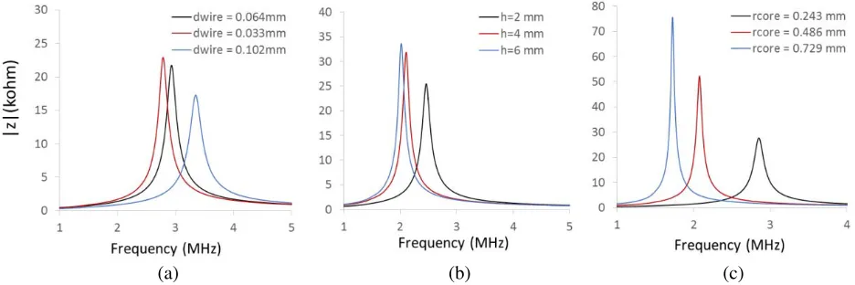
Figure 8. Parameters in investigation (a) wire diameter of the coil loop, (b) the height of ferrite shielding and ferrite core and (c) radius of ferrite core.
higher Q-factor than the other. But the drawback is that the frequency moves to lower value in these configurations.
Figure 8(a) shows different wire diameter parameters used for wire loop of the coil. The diameter that we use here is available in the market for probe fabrication. The result shows that the thicker wire has moved the resonance frequency to larger band. However, the Q-factor of such a diameter value is decreased. Fig. 8(b) shows that the height of ferrite core and shielding varies from 2 to 6 mm which is investigated. The result shows that the resonance frequency shifts to lower band with higher h value, and it will lead to saturation for higher height. Fig. 8(c) shows various ferrite core diameters under investigation. The resonance frequency shifts to lower band with Q-factor increase when the larger diameter of core is used. The magnetic fields generated by the coil concentrate inside the core due to the ferrite’s ability to attract magnetic flux for noise countermeasures. The ability of noise countermeasure increases with larger diameter of core.
6. CONCLUSIONS
of EC probe, which complements, rather than competes with, testing and measurement, will not only reduce the prototypes cost, but also offer more physical insight into the behavior of the inspection system. Enhanced detection sensitivity via resonant peak (up to ∼ 300%) and frequency shifting (∼0.02 MHz) for electrical discharge machining (EDM) notch can be captured in the simulation model via an EM circuit co-simulation. The modeling and experimental results of electrical resonance eddy current testing for the detection of surface-breaking in titanium alloys are compared in good agreement with each other. Investigation of both experiment and modeling is desirable to develop a precise calibrated model for simulation that could provide the compensation factors for different types of eddy current probe. However, it should be noted that the sensitivity of the probe may be affected by a number of environmental factors such as temperature, humidity and nature of tested material such as degree of surface roughness. At this point, such issues could not be taken into consideration in our simulation model and will be addressed by using Probability of Detection (PoD) approach. Such implementation could lead to substantial improvement of the inspection procedures in NDT.
REFERENCES
1. Blitz, J., Electrical and Magnetic Methods of Non-destructive Testing, 2nd Edition, Springer-Science+Business Media Dordrecht, 1997.
2. Bowler J. R., S. J. Norton, and D. J. Harrison, “Eddy-current interaction with an ideal crack I. The forward problem,”J. of Appl. Phys., Vol. 75, 8138–8144, 1994.
3. Sophian, A., G. Y. Tian, D. Taylor, and J. Rudlin, “Design of a pulsed eddy current sensor for detection of defects in aircraft lap-joints,” Sensors and Actuators A: Physical, Vol. 101, Nos. 1–2, 92–98, 2002.
4. Ball, D. L., “The role of nondestructive testing in aircraft damage tolerance,” Materials Evaluation, Vol. 61, No. 7, 814–818, 2003.
5. Hashizume, H., Y. Yamada, K. Miya, S. Toda, K. Morimoto, Y. Araki, K. Satake, and N. Shimizu, “Numerical and experimental analysis of eddy current testing for a tube with cracks,”IEEE Trans. Magn., Vol. 28, 1469–1472, 1992.
6. Thollon, F., B. Lebrun, N. Burais, and Y. Jayet, “Numerical and experimental study of eddy current probes in NDT of structures with deep flaws,”NDT & E Int., Vol. 28, 97–102, 1995. 7. Perrusson, G., P. Vafeas, and D. Lesselier, “Low–frequency dipolar excitation of a perfect ellipsoidal
conductor,”Quarterly of Applied Mathematics, Vol. 68, 513–536, 2010.
8. Vafeas, P., P. K. Papadopoulos, and D. Lesselier, “Electromagnetic low–frequency dipolar excitation of two metal spheres in a conductive medium,” Journal of Applied Mathematics, Vol. 2012, 1–37, 2012.
9. Bernieri, A., G. Betta, L. Ferrigno, and M. Laracca, “Crack depth estimation by using a multi-frequency ECT method,” IEEE Trans. on Instrumentation and Measurement, Vol. 62, 3, 2013. 10. Chady, T. and R. Sikora, “Optimization of eddy-current sensor for multifrequency systems,”IEEE
Trans. Magn., Vol. 39, 1313–1316, 2003.
11. Yin, W., P. J. Withers, U. Sharma, and A. J. Peyton, “Non-contact characterisation of carbon-fibre-reinforced plastic using multi-frequency eddy-current sensors,” IEEE Trans. on Instrumentation and Measurement, Vol. 62, 3, 2007.
12. Hughes, R. and S. Dixon, “Developments in near electrical resonance signal enhancement (NERSE) eddy-current methods,”Progress in Quantitative NDE, Vol. 1650, 345–352l, 2015.
13. Hughes, R., Y. Fan, and S. Dixon, “Near electrical resonance signal enhancement (NERSE) in eddy-current crack detection,” NDT &E International, Vol. 66, 82–89, 2014.
14. Kincaid, T. G. and M. V. K. Chari, “The application of finite element method analysis to eddy current NDE,” Proceedings of the ARPA/AFML Review of Progress in Quantitative NDE, July 1977–June 1978.
16. Bui, V. P., C. Lane, Y. L. Hor, Z. Yu, and C. E. Png, “Model-assisted NDT for sub-mm surface-breaking crack detection in alloys,” 2017 XXXIInd URSI GASS, 1–4, 2017.
17. Burke, S. K., “Eddy-current inversion in the thin-skin limit: Determination of depth and opening for a long crack,” J. of Appl. Phys., Vol. 75, 3072–3080, 1994.
18. Aldrin, J. C., et al., “Model-based inverse methods for sizing cracks of varying shape and location in bolt-hole eddy current (BHEC) inspections,” AIP Conference Proceedings, Vol. 1706, 090020, 2016.
19. Vafeas, P., A. Skarlatos, T. Theodoulidis, and D. Lesselier, “Semi-analytical method for the identification of inclusions by air-cored coil interaction in ferro-magnetic media,” Mathematical Methods in the Applied Sciences, Vol. 41, 6422–6442, 2018.
20. Chew, W. C., “Waves and fields in inhomogeneous media,”IEEE Press Series in Electromagnetic Waves, IEEE Press, 1995.
21. Cheney, W. and D. Kincaid, Numerical Mathematics and Computing, 4th Edition, 138–141, Brooks/Cole, 1999.
22. Hor, Y. L., Y. Zhong, V. P. Bui, and C. E. Png, “Electrical resonance eddy current sensor for submillimeter defect detection,” Proc. SPIE, Nondestructive Characterization and Monitoring of Advanced Materials, Aerospace, and Civil Infrastructure, 2017.