High Performance ADDLL using DDFF Based
Frequency Divider and Counter
Dhanya Simon
1, K.T Mathew
2PG Student [VLSI], Dept. of ECE, Viswajyothy College of Eng ineering & Technology, Vazha kula m ,Kera la, India1
Professor, Dept. of ECE, Viswa jyothy College of Engineering & Technology, Va zhakula m , Ke rala , Ind ia2
ABSTRACT: In many areas, the Delay-Locked Loop (DLL) can be an alternative to the traditional frequency generation technique - the Phase-Locked Loop (PLL). The DLL is preferred because of its better stability, sma lle r jitter accumulat ion, and shorter locking time , as co mpared to the PLL. Since using the high performance DDFF in the design of counter, frequency divider, and phase detector, can achieve high performance DLL with min imu m power consumption. The performance will be analysed with the ADDLL based on conventional flip -flop and XCFF. This project presents the design and imp le mentation of high performance ADDLL using DDFF based frequency divider and counter with minimu m power de lay product . In this project, design of frequency mu ltiplier using DDFF based ADDLL which mu ltip lies the frequency of output wave by factors of 8 is done
.
The circuit is imp le mented in 180n m technology using cadence virtuoso software.
KEYWORDS: Flip_Flop, DDFF, ADDLL.
I.INTRODUCTION
In many areas, the Delay-Locked Loop (DLL) can be an alternative to the traditional frequency generation technique - the Phase-Locked Loop (PLL).In ADDLL it is possible to stop any toggling, thus no dynamic power is consumed .The area of ADDLL is typically much lo wer than that of analog DLLs. The main reason is the large filte ring capacitors used in analog DLLs/PLLs. Typical A DDLLs require fe w thousands gates, and their area is scaled at each technology generation .
Technology and speed are always moving forwa rd, fro m low scale integration to large and VLSI and fro m megahertz (MHz) to gigahertz (GHz). The system require ments are also rising up with this continuous advancing process of technology and speed of operation.The proposed DDFF eliminates the redundant power dissipation present in the XCFF. Hybrid latch flipflop (HLFF) and semi dynamic flip flop (SDFF) are considered as the classic high -performance flip-flops. They possess a hybrid architecture that combines the merits of dynamic and static structures. In addition, SDFF has a distinctive capability of incorporating logic very effic iently, because unlike the true single phase latch (TSPC) ,on ly one transistor is driven by th e data input. This greatly helps in reducing the pipeline overhead since the delay and area associated with one or mo re logic stages preceding the flip -flop can be eliminated. Several hybrid flip-flop designs have been proposed in the past decade, all aiming at reduction of power, delay.
A recent paper introduced a flip-flop architecture named cross charge control flip-flop (XCFF), which has considerable advantages over SDFF and HLFF in both power and speed. It uses a split -dynamic node to reduce the precharge capacitance, which is one of the most important reasons for the large power consumption in most of the conventional designs. But this structure still has some drawbacks, due to redundant power dissipation that results when the data does not switch for more than one clock (CLK) cycles. Also, the large hold -t ime require ment makes the design of timing-critica l systems with XCFF an involved process. Finally, despite having a single data -driven transistor, embedding logic to XCFF is not very efficient due to the susceptibility to charge sharing at the internal dynamic nodes.
ADDLL showed that it exhibits lower power dissipation along with comparable speed performances. So when using the low power and delay flip flop the entire power consumption of the circuit can be reduced .Since the delay locked loop have a delay adjustment cell , but using the low delayed flip-flop based modules we can reduce the total delay of circuit without affecting the ADDL working.
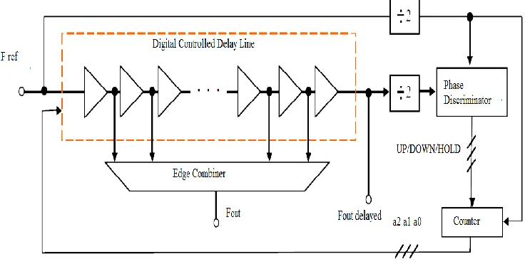
This paper proposes a High performance ADDLL a rchitecture has the phase detector subsystem and the up/down counter subsystem using the high performance DDFF . The imple mentations of the DLL can be categorized by its delay ele ments which can be continuously variable or analog, discretely ordered/continuous or analog -digital, or a ll-dig ital. Due to all d igital co mponents it consumes very low powe r. To incorporate the digita l configurat ion the charge pump was replaced by a counter. The total system consists of a phase detector, an up/down counter, the delay line, clock divider, and the frequency multip lie r. The frequen cy mult iplying technique is performed by using an edge combiner based clock synthesis system. The ADDLL arch itecture has the phase detector subsystem generates an up/down signal based on the phase difference between reference clock and the delayed version of the clock fro m the Bit controlled Delay line bloc k. The up/down counter subsystem counts either up or down based on the signal fro m the phase detector. The low frequency clock to the counter subsystem is generated by the clock divider subsystem. The clo ck divider subsystem generates a clock frequency of the output of the counter controls the load of the delay ele ments in the delay line.
II
.
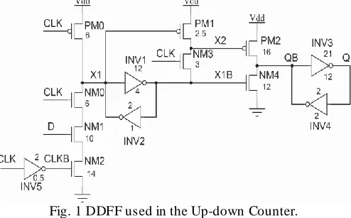
DDFF ARCHIT ECTUREFig 1 shows the DDFF arch itecture. Node X1 is pseudo-dynamic, with a weak inverter acting as a keeper, whereas, compared to the XCFF, in the new architecture node X2 is purely dynamic . An unconditional shutoff mechanis m is provided at the frontend instead of the conditional one in XCFF. The opera tion of the flip-flop can be divided into two phases: 1) the evaluation phase, when CLK is high, and 2) the precharge phase, when CLK is low. The actual latching occurs during the 1–1 overlap of CLK and CLKB during the evaluation phase. If D is high prior to this overlap period, node X1 is discharged through NM0-2. Th is switches the state of the cross coupled inverter pair INV1-2 causing node X1B to go high and output QB to discharge through.NM4. The low level at the node X1 is reta ined by the inverter pair INV1-2 fo r the rest of the evaluation phase where no latching occurs. Thus, node X2 is held high throughout the evaluation period by the pMOS transistor PM1. As the CLK fa lls lo w, the circuit enters the precharge phase and node X1 is pulled high through PM0, switching the state of INV1-2. During this period node X2 is not actively driven by any transistor, it stores the charge dynamica lly. The outputs at node QB and ma intain their voltage levels through INV3-4. If D is zero prior to the overlap period, node X1 rema ins high and node X2 is pulled low through NM3 as the CLK goes high. Thus, node QB is charged high through PM2 and NM4 is held off. At the end of the evaluation phase, as the CLK fa lls low, node X1 re ma ins high and X2 stores the charge dynamically. The a rchitecture e xhib its negative setup time since the short transparency period defined by the 1–1overlap CLK of and CLKB a llows the data to be sampled even after the rising edge of the CLK before CLKB fa lls low.
Fig. 1 DDFF used in the Up-down Counter.
threshold well be low the wo rst case voltage drop at node X1 due to charge sharing. The DDFF have low powe r, less charge sharing at internal node, low powe r delay product .so DDFF is used in the design of ADDLL.
III.ADDLL ARCHITECTUR E
Control part of the ADDLL consists of the phase discriminator, delay controlled delay line and counter .Outputs of the delay line and the reference signal are fed into the phase discriminator. When the phases of these two signals are mis matched, phase discriminator produces either an up signal or down signal, depending on the phase lag of the reference or delayed signal. Digita l types of phase discriminators operate on the binary signals exclusively, and are usually combined with a m-bit binary UP/DOWN/ HOLD counter that replaces the analog charge pump and the loop filter of the analog DLL. When the delay of the DE has to be increased/decreased (phase mis match), the PD generates the UP/DOWN signal, which inc re ments/decrements m bit counter
.
A frequency divider is a circuit that takes an input signal of a frequency fin and generates an output signal of a frequency fout, wherefout=fin/n and ‗n‖ is an integer. Digital dividers can work up to tens of GHz.They can be used for improving the performance of electronic counter measures equipment.Fig. 2 A ll-dig ital DLL
Fig.3 Phase discriminator(PD)
The Digital-Controlled De lay Ele ment (DCDE) is based on the MUX structure (Fig. 4 illustrates the case of m = 3). According to the combination of them control bits [am−1 2 ...a1,a0] generated in the counter of the phase discriminator, mu ltip le xers seria lly co mbine binary-we ighted LCELL de lays, resulting with the follo wing delay incre ments
.
Fig.4 Digita l-Controlled De lay Ele ment (DCDE) fo r m = 3
The Digita l Controlled Delay Line (DCDL) consists of n serially connected DCDE (Fig. 5 illustrates the case of n =8). So, the ma xima l mu ltip licat ion factor can be equal to fOUTMAX = nfREF.. The DCDL is the most important part of an ADDLL design, as it decides the operating frequency range, delay resolution and delay linearity of the ADDLL.
Fig.5 Digita l-Controlled De lay Line (DCDL) fo r n = 8
Fig.6 Edge comb iner (EC)
The ADDL using DDFF based frequency divider and counter performance is analy zed using cadence virtuoso software in 180 nm technology . the ADDL using DDFF is compared with the performance of ADDL using XCFF and conventional flip-flop ie NAND based D flip flop.
V. RES ULT AND DISCUSS ION
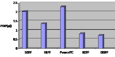
Table 1 illustrates the speed and power delay product (PDP) of various flip -flops at 50% data activ ity. The results show that the Dual Dyna mic flip-flop has the lowest PDP a mong the group and uses least number of devices .
Table 1 Performance Co mparison of various flip-flops
Fli p-flop Number of transistors Total power (mw) Mi ni mum D-Q(ps) PDP(pj)
SDFF 23 25.138 80.98 2.03
HLFF 20 13.806 99.07 1.367
Power PC 603 22 22 104.1 2.29
XCFF 21 7.98 101.8 0.812
DDFF 18 7.7 94.25 0.725
The chart Fig. 7shown below is the PDP analysis of flip-flop under study. The Dual Dynamic flip-flop has the lowest
PDP a mong the group.
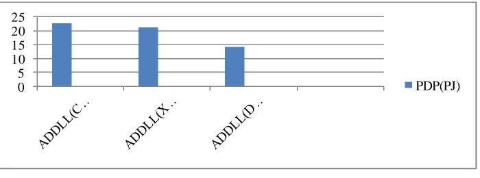
Table. 2 illustrates the speed and power delay product (PDP) of ADDLL using different flip -flops at 50% data activity.
The results show that the ADDLL using Dual Dyna mic flip -flop has the lowest PDP a mong the group.
Table .2 Pe rformance Co mparison of various ADDLL
ADDLL Total Powe r (mw) Delay (ns) PDP(pj)
ADDLL(Conventional) 25.35 0.9 22.8
ADDLL(XCFF) 15.8 1.35 21.33
ADDLL(DDFF) 13.1 1.104 14.46
The chart Fig. 8shown below is the PDP ana lysis of ADDLL under study. The ADDL using Dual Dynamic flip -flop has the lowest PDP a mong the group.
Fig. 8 PDP analysis of ADDLL under study.
The matching between the parallel paths of the EC is degraded by the random local variations. To demonstrate the device mis match effects on EC performance, simulat ions are carried out on the la yout extracted vie w of the EC with symmetric logic gates. The matching between the transistors can be improved by increasing their size Simu lations for ECs with different transistor widths are performed to study the improve ment .
VI.CONCLUS ION
The ADDLL is preferred because of its better stability, sma lle r jitter accumu lation, and shorter locking time, as compared to the PLL. Since using the high performance DDFF in the design of counter, frequency divider, and phase detector, can achieve high performance DLL with minimu m power consumption. If mo re advanced technologies were used, the performance of the DLL such as operating frequency range and jitters could be improved with a little design effort. The power consumption and the total die area would be redu ced as well. The circuit is imple mented in 180n m technology. And the performance is analyzed with the DLL based on conventional flip -flop and XCFF flip-flop. ADDLL using DDFF flip-flop has the lowest PDP.
REFER ENC ES
[1] Tomislav ˇSvedek — Tomislav Mati´c — Marijan Herceg PldModeling Of All digital DLL Journal of Electrical Engineering, Vol. 60, No. 5, 2009, 246–254
[2] KalarikkalAbsel, Lijo Manuel, and R. K. Kavitha, Member, IEEE, ―Low- Power Dual Dynamic Node Pulsed Hybrid Flip-Flop Featuring Efficient Embedded Logic,‖ IEEE transactions on very large scale integration (vlsi) systems, vol. 21, no. 9, september 2013
[3] A. Hirata, K. Nakanishi, M. Nozoe, and A. Miyoshi, ―The cross charge control flip flop: A low-power and high-speed flip-flop suitable for mobile application SoCs,‖ in Proc. Symp. VLSI Circuits Dig. T ech. Papers, Jun. 2005, pp. 306–307
[4] Hsiang-Hui Chang, Student Member, IEEE, and Shen-Iuan Liu, Senior Member, IEEE‖A Wide-Range and Fast -Locking All-Digital Cycle-Controlled Delay-Locked Loop ― IEEE Journal Of Solid-State Circuits, Vol. 40, No. 3, March 2005
[5] Bum-SikKim and Lee-Sup Kim ―100M Hz all-digital delay -locked loop for lowpower application‖ Electronics Letkers3rd September 1998 Vol. 34 No. 18
[6] Chia-Yu Yao, Member, IEEE, Yung-Hsiang Ho, Yi-Yao Chiu, and Rong-Jyi Yang, Member, IEEE― Designing a SAR-Based All-Digital Delay-LockedLoop With Constant Acquisition CyclesUsing a Resettable Delay Line‖ IEEE Transactions On Very Large Scale Integration (VLSI) Systems