MASTER THESIS
HARDWARE
ACCELERATOR
SHARING WITHIN AN
MPSOC WITH A
CONNECTIONLESS
NOC
Gerben Wevers
DEPARTMENT OF ELECTRICAL ENGINEERING, MATHEMATHICS AND COMPUTER SCIENCE
COMPUTER ARCHITECTURES FOR EMBEDDED SYSTEMS EXAMINATION COMMITTEE
University of Twente
Master Thesis
Hardware Accelerator Sharing
within an MPSoC with a
connectionless NoC
Author:
G.G.A. Wevers
Student number:
s0144053
Committee:
Prof. dr. ir. M.J.G Bekooij
Dr. ir. J.F. Broenink
B.H.J Dekens, Msc
Research Group Computer Architecture for Embedded Systems,
Department of EEMCS University of Twente, Enschede, The
Abstract
For the last decades, increasing the computational performance of a micropro-cessor chip was mainly achieved by scaling transistor sizes. Not only can more transistors be placed in a single die, smaller transistors allow higher clock fre-quencies. While transistor sizes are still decreasing, designers are facing mayor power consumption issues which prevent further performance improvements by simply increasing clock frequencies. A clear trend is visible where multiple cores are added to the same chip to form so-called multi-core systems.
The same trend is visible in the embedded systems domain where System-on-Chips (SoCs) are transformed into Multi-Processor System-on-System-on-Chips (MPSoCs). An MPSoC can either be homogeneous (consisting of identical processing ele-ments) or heterogeneous (consisting of different types of processing elements, e.g. Central Processing Units (CPUs) and weakly programmable hardware ac-celerators). Communication between the processing elements is taking place via a Network-on-Chip (NoC).
At the University of Twente multiple researchers are working on an MPSoC called Starburst. The main characteristics of this platform are: (1) the Star-burst platform is a scalable distributed shared memory many-core system, (2) it targets real-time streaming applications where firm real-time requirements are assumed and (3) the set of applications to be run on the platform (and thus the communication pattern) is unknown at design time, which requires the platform to be flexible.
The Starburst platform was originally designed as a homogeneous MPSoC con-sisting of multiple identical soft-core CPUs. As a case study a Phase Alter-nating Line (PAL) video decoding application was mapped onto the platform. The demonstrator produced a video quality far from commercially acceptable and for some operations multiple parallel executing CPUs were required. This case study showed that the computational power was simply limited by the per-formance of the CPUs in the system. In order to improve the computational performance of the Starburst platform weakly programmable hardware acceler-ators were added, which transformed Starburst from a homogeneous MPSoC to a heterogeneous MPSoC.
to execute on the same platform.
We solved this problem by implementing a centralized component called a gate-way. The gateway is used to buffer multiple incoming data streams, and to push packets of data at high speed sequentially through the accelerators. Most accel-erators have a configuration and/or state. Context switches are applied where the configuration and state for a certain data stream is loaded into the accel-erator and extracted after a specific number of samples have been processed. A dataflow model of the sharing mechanism is constructed, which allows us to give real-time guarantees such as latency and throughput.
Acknowledgements
First of all, I would like to thank Marco for the numerous discussions we had and feedback I have received during my research. I highly appreciate his critical view on my ideas and solutions, and the discussions we had on the dataflow models, as it took some time to get them right.
I would like to thank Berend for the daily supervision, as he was always available to answer my questions. More than once I walked into his office with just a single simple question eventually leaving the room an hour later after discussing lots of new ideas for my project. I really liked his enthusiastic approach when brainstorming these new ideas or solving the numerous problems I encountered with the Starburst or Xilinx tooling.
Additionally I would like to thank Jochem Rutgers (who recently received his doctorate degree) as he originally designed and developed the Starburst plat-form. I could always ask him for help when annoying bugs popped up.
I would like to finish by thanking Lisanne, my girlfriend, for supporting and mo-tivating me throughout this project. Without her finishing my master’s thesis would be much, much harder.
Gerben Wevers
Contents
Abstract i
Acknowledgements iii
Contents v
List of Figures ix
List of Tables xiii
Acronyms xv
1 Introduction 1
1.1 Context . . . 1
1.2 Research platform . . . 3
1.3 Problem Description . . . 7
1.4 Research Questions . . . 9
1.5 Contributions . . . 10
1.6 Outline . . . 11
2 Related Work 13 2.1 Hardware accelerator architectures . . . 13
2.2 Real-time analysis models . . . 16
2.3 Arbitration . . . 17
2.4 State of the Art . . . 19
2.5 Summary . . . 21
3 Starburst Platform 23 3.1 Hardware Platform . . . 23
3.2 Starburst . . . 24
3.2.1 Processing tile . . . 25
3.2.2 Linux tile . . . 26
3.2.3 Warpfield . . . 27
3.2.4 Nebula ring . . . 28
3.2.5 Hardware Accelerator integration . . . 29
3.3 Software . . . 31
3.3.1 Helix kernel . . . 32
3.3.2 CFIFO . . . 32
List of Figures
1.1 High level overview of the Starburst platform (the arrows indicate
master/slave relations) . . . 4
1.2 Schematic overview of the Nebula ring . . . 5
1.3 Schematic overview with one hardware accelerator, connected to the Nebula ring interconnect . . . 6
2.1 Hardware Accelerator integration using Instruction Set Extension 13 2.2 Hardware Accelerator integration using a Remote Procedure Call 14 2.3 Stream processing hardware accelerators . . . 15
2.4 Task scheduled under TDM with a fixed budget B (in red) during a period P (in blue) . . . 18
2.5 Single actor dataflow model . . . 18
2.6 Execution of a task during its time slices . . . 19
3.1 ML605 development board . . . 24
3.2 High level overview of the Starburst platform. Arrows indicate master-slave relations. . . 25
3.3 Processing tile . . . 26
3.4 Linux tile . . . 27
3.5 Schematic overview of the Nebula ring . . . 29
3.6 Schematic overview of two processing tiles and one hardware ac-celerator, connected to the Nebula ring interconnect . . . 31
3.7 Schematic overview of two processing tiles and one hardware ac-celerator, connected to the Nebula ring interconnect. . . 32
3.8 CFIFO administration overview . . . 33
4.1 Hardware Accelerator pipeline . . . 35
4.2 Hardware Accelerator pipeline with duplicated registers . . . 36
4.3 Hardware Accelerator sharing via gateways . . . 37
4.4 Non-preemption example: a gateway and a consumer are com-municating data via a Hardware Accelerator . . . 38
4.5 CSDF graph of an accelerator pipeline . . . 40
5.1 Accelerator Interface . . . 45
5.2 Gateway overview, including Accelerator Interface . . . 45
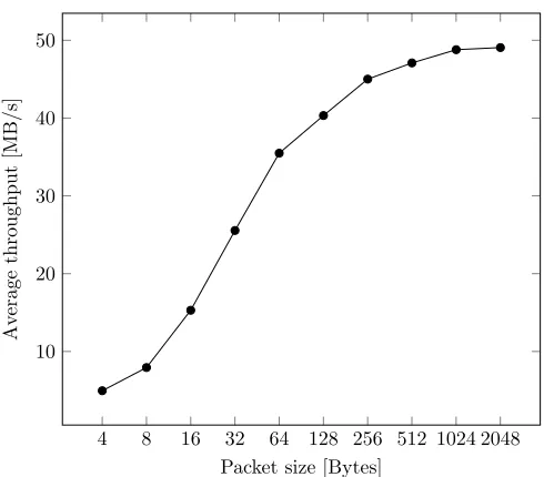
5.3 CFIFO performance measurements . . . 47
5.4 Gateway overview, including DMA Controller . . . 48
5.5 Schematic overview of the RingDMA controller . . . 49
List of Tables
3.1 Rule set Nebula ring router . . . 30
7.1 Hardware usage of reference components . . . 77 7.2 Hardware usage Networking Components. The percentages show
the relative size compared to a Starburst MicroBlaze . . . 78 7.3 Hardware usage Accelerator Interface. The percentages show the
relative size compared to a Starburst MicroBlaze . . . 78 7.4 Hardware usage Ringshell. The percentages show the relative size
compared to a Starburst MicroBlaze . . . 78 7.5 Hardware usage DMA-controller(s). The percentages show the
relative size compared to a Starburst MicroBlaze . . . 79 7.6 Hardware usage Exit Gateway. The percentages show the relative
size compared to a Starburst MicroBlaze . . . 80 7.7 Combined hardware usage of all required components . . . 80 7.8 Hardware usage CORDIC. The percentages show the relative size
compared to a Starburst MicroBlaze . . . 84 7.9 Hardware usage FIR Filter. The percentages show the relative
Acronyms
ℒℛ Latency-Rate.
ADC Analog to Digital Converter.
ASIC Application-Specific Integrated Circuit.
BE Best Effort.
BRAM Block Ram.
CF Compact Flash.
CFIFO C-HEAP FIFO.
CORDIC Coordinate Rotation Digital Computer.
CPU Central Processing Unit.
CRC Cyclic Redundancy Check.
CSDF Cyclo-Static Dataflow.
DAB Digital Audio Broadcasting.
DDR3 Double Data Rate type 3 SDRAM.
DMA Direct Memory Access.
DSP Digital Signal Processor.
DSP48E1 Digital Signal Processing Element.
EM Event Models.
FCFS First-come, First-served.
FIFO First-in, First-out.
FIR Finite Impulse Response.
FPGA Field-Programmable Gate-Array.
FPU Floating Point Unit.
FSL Fast Simplex Link.
GAM Global Accelerator Manager.
GS Guaranteed Service.
HD High Definition.
HSDF Homogeneous Synchronous Dataflow.
IIR Infinite Impulse Response.
IP Intellectual Property.
IPIC Intellectual Property Interconnect.
ISE Instruction Set Extension.
L2 Level-2.
LMB Local Memory Bus.
LUT Look-Up Table.
LUTRAM LUT RAM.
MCM Maximum Cycle Mean.
MMU Memory Management Unit.
MPMC Multi-Port Memory-Controller.
MPSoC Multi-Processor System-on-Chip.
NI Network Interface.
NoC Network-on-Chip.
OO Object Oriented.
OPB On-chip Peripheral Bus.
PAL Phase Alternating Line.
PLB Processor Local Bus.
POSIX Portable Operating System Interface.
RISC Reduced Instruction Set Computer.
RNG Random Number Generator.
ROM Read-Only Memory.
ROSPS Rate Optimal Static Periodic Schedule.
RPC Remote Procedure Call.
RR Round-Robin.
RTC Real-time Calculus.
SDF Synchronous Dataflow.
SDR Software Defined Radio.
SoC System-on-Chip.
SPM Scratchpad Memory.
SPS Static Periodic Schedule.
SSE Streaming SIMD Extensions.
STS Self-Timed Schedule.
TDM Time-Division Multiplexing.
UART Universal Asynchronous Receiver/Transmitter.
UHD Ultra High Definition.
UML Unified Modeling Language.
USB Universal Serial Bus.
Chapter 1
Introduction
1.1
Context
When Intel invented the microprocessor in 1971, probably no one would have expected the impact it would have and unimaginable evolution it would go through in the upcoming decennia. Starting with a clock speed of 740 kilohertz and equipped with a mere 2300 transistors, 43 years later the latest Intel Haswell chips have around 1.4 billion transistors, operating on clock-speeds of several gigahertz.
The demand for such increases can be explained by looking at for example the domain of consumer electronics, such as video or audio applications. New standards such as Digital Audio Broadcasting (DAB), its successor DAB+, High Definition (HD) video (at a resolution of 1920×1080 pixels) and its successor Ultra High Definition (UHD) or 4K video (at a resolution of 3840×2160 pixels) clearly explain the demand for embedded systems with enough computing power to run these applications. The fact that a lot of these embedded systems are battery powered (e.g. mobile phones) explains why power efficiency is a second import requirement.
For the last decades, increasing the computational performance of a micropro-cessor chip was mainly driven by scaling transistor sizes. Reducing the size of a transistor has three important benefits [7]:
1. When reducing the dimension of a transistor, its total area reduces quadratic. E.g. a reduction of 30% (×0.7) in dimension, corresponds to a 50% shrink in area (×0.72). Or, as Moore‘s law dictates, allows the number of tran-sistors to double.
2. A smaller transistor allows a higher clock frequency, due to lower internal delays. Increasing the clock-frequency directly improves the computa-tional performance.
3. A smaller transistor requires less power to operate on.
important requirement in order to give real-time guarantees. The analysis of heterogeneous designs is becoming increasingly complex, when multiple types of processing units (with different programming models), connected via some sort of interconnect, are added to the system. It is important to maintain as much analyzability per processing unit as possible. During this research an existing heterogeneous MPSoC will be modified. The most important requirement of these modifications is the fact that this happens while preserving analyzability.
1.2
Research platform
The previous section explained the context of this research. This section will focus on the research platform, in order to understand and formulate the prob-lem description. Afterwards, the platform will be discussed in more detail in Chapter 3.
At the University of Twente multiple researchers are working on an MPSoC called Starburst. The main characteristics of this platform are [23]:
∙ The platform is a scalable distributed shared memory many-core system.
∙ The Starburst platform targets real-time streaming applications where
firm real-time requirements are assumed. Deadline misses are highly un-desirable but not catastrophic.
∙ The set of applications to be run on the platform (and thus the communica-tion pattern) is unknown at design time. For this reason, the architecture must be flexible.
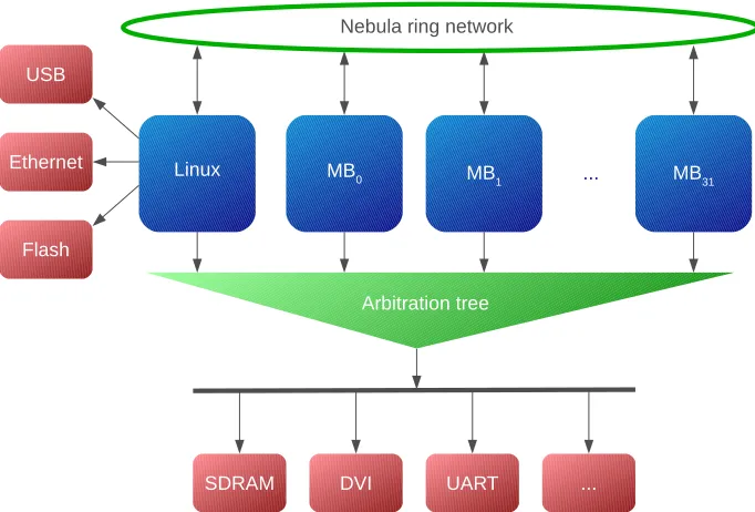
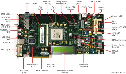
The Starburst MPSoC is being developed on a Xilinx ML605 development board. This development board is equipped with a Virtex-6 Field-Programmable Gate-Array (FPGA). A high level overview of the platform is given in Figure 1.1.
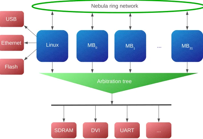
The platform consists of a power-of-two number of processing tiles. The pro-cessing tiles, also called MicroBlaze tiles, are equipped with a Xilinx MicroBlaze CPU, and are denoted with MBx in Figure 1.1. The figure displays a 32-core
configuration, which is currently also the maximum given the FPGA resources. One additional processor is added to the platform, running embedded Linux. This processor is connected to (and in control of) several on-board peripher-als like the Ethernet port or the Universal Serial Bus (USB) controller. The linux core is therefore mainly used for interaction with the environment. The processors are so-calledsoftcoreCPUs, which can be fully implemented in recon-figurable hardware by the logic synthesis tools. Due to this reconfigurability it is possible to configure the CPU at design time, where different components like a Floating Point Unit (FPU), barrel shifter, hardware multiplier or hardware divider may be added to the system.
Figure 1.1: High level overview of the Starburst platform (the arrows indicate master/slave relations)
facilitates communication on the platform. The interconnect consists of two separate parts. The first part is the Warpfield arbitration tree which makes communication from and to shared resources like external Double Data Rate type 3 SDRAM (DDR3) memory possible. This is a latency-critical channel, where the performance of the platform directly degrades with a higher latency. Take for example a read operation from external DDR3 memory. When one of the CPUs issues a read operation, this CPU has to wait until its instruction has propagated through the complete interconnect, data is fetched out of memory and is propagated back through the interconnect before the CPU can continue with its computation. Meanwhile stall cycles are inserted in the pipeline of the CPU which results in a degradation of performance. For this reason the latency introduced by the arbitration tree is kept as low as possible. The arbitration tree provides a slave interface to each Microblaze in the system. When a Mi-croblaze issues a read- or write-request this request is packetized and is given a timestamp and source ID. The packets enter a binary tree where at each step local arbitration based on the timestamp is applied. This way arbitration is applied according to a First-come, First-served (FCFS) policy, where a packet with the lowest timestamp is allowed to proceed first.
topol-ogy with a very small area footprint [13]. Figure 1.2 gives an overview of the Nebula ring network. This figure shows that each CPU is connected via a Network Interface (NI) to a router, and each router is connected to its two neighbouring routers to create a ring-like structure. In the same figure the prin-ciple of executing a streaming application on the platform is depicted. Together the processors are processing a stream of data, by sending the results of their computation to another processor in the system, creating a chain of processors.
Figure 1.2: Schematic overview of the Nebula ring
As discussed in the previous section, the Starburst platform targets (real-time) streaming applications. A key advantage of streaming applications is the fact that they usually are latency insensitive, which means that the latency intro-duced by the communication channel has no influence on the performance of the complete system, if the throughput of the communication channel is high enough. Latency is a fundamental problem in digital circuit design because of the limited speed at which a signal by definition can travel. With digital circuits becoming increasingly larger, signals have to travel larger distances. But also when clock frequencies are increasing, the latency (expressed in the number of clock cycles) will increase. The Nebula ring network tries to exploit thislatency
insensitive property by only supporting posted write actions; a CPU does not
have to wait on data being accepted by a receiver, instead the processor can immediately continue with its computations when data has been placed on the ring interconnect without having to insert stall cycles. Lossless communica-tion, which guarantees that no data will be dropped during communicacommunica-tion, is achieved in the software layers running on top of the hardware platform. Ba-sically, after writing a packet to another processing tile, the receiving tile will write a message back, to acknowledge that the sending tile can write a new packet.
applications have been mapped onto it. One of these applications is a PAL video decoder [13], which is a good example of a streaming application, where a sequence of computations has to be applied on the incoming stream of data. This case-study showed that the processing power of the homogeneous Starburst platform was simply limited by the computational power of the general purpose CPUs in the system. For example, the video decoder required four (out of 32) fully utilized CPUs to do one specific operation (I/Q amplitude detection).
Hardware acceleration
A commonly used technique to improve the performance of computationally ex-pensive functions is to accelerate them using hardware accelerators. Hardware accelerators are dedicated pieces of hardware designed for one specific operation. By using hard-wired implementations the overhead of general purpose architec-tures is avoided, which results in increased performance and energy efficiency by orders of magnitude compared to an implementation on a general purpose architecture [17]. In [16] support for hardware accelerators was added to the Starburst platform. With this addition the Starburst platform changed from an homogeneous architecture to a heterogeneous architecture consisting of a mix of identical processors and a set of weakly programmable hardware accelerators.
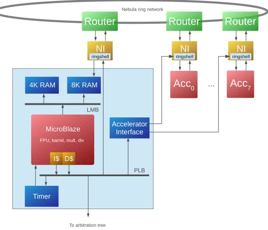
Figure 1.3: Schematic overview with one hardware accelerator, connected to the Nebula ring interconnect
its computation it will forward the result to a second CPU. As discussed, loss-less communication between CPUs is achieved in the software layers running on the processors. For the hardware accelerators another form of flow-control was required, this is because they are unaware of memory addresses and have no software running which manages communication.
Credit-based flow-control was implemented for this purpose. Chapter 3 will focus on this communication protocol in more detail, for now only the ba-sic principle will be explained. Every hardware accelerator is equipped with a hardware-based First-in, First-out (FIFO)-buffer. Credits are denoting the number of free buffer positions in this FIFO-buffer. Processing tiles are only allowed to send data to a hardware accelerator if they have at least one credit, which corresponds to free space in the FIFO-buffer. When the hardware accel-erator accepts a data sample, a credit is sent back over an additionalcredit-ring
(see Figure 1.3) to the corresponding processing tile.
When a hardware accelerator receives a data sample, it is unable to determine the sender or the recipient; this information is simply not embedded in the data stream. Instead, the NIs to which the hardware accelerators are connected are programmed to give them the required knowledge. One register holds the memory address to which the accelerator has to forward its computed results, a second register holds the memory address to which credits have to be returned, furthermore a counter is implemented to keep track of the number of credits. This is an important property; a processor has to configure the hardware accel-erator before the stream of data can be processed by the accelaccel-erator.
As a case-study, the PAL video decoder was modified, where the computation-ally expensive I/Q amplitude detection operation was implemented in hardware. This case-study showed some interesting results; mapping this specific opera-tion on an hardware accelerator freed four CPUs, while the performance of this specific operation increased by 366%.
1.3
Problem Description
The previous two sections described the context of this research, and gave a high level overview of the research platform. This section will describe the problem in more detail.
∙ How to handle multiple configurations and states for a hardware acceler-ator?
∙ Is it possible to increase the currently low utilization of the hardware accelerators via hardware accelerator sharing?
∙ Which techniques can reduce the overhead introduced by switching be-tween data-streams?
∙ What additional hardware is required to share hardware accelerators, and can this additional hardware be justified by the amount of hardware saved by sharing hardware accelerators?
∙ Can a (detailed) dataflow model of this sharing protocol be constructed, and related to that, can an abstraction of this dataflow model be created, which is easier to use at the cost of a less accurate dataflow model?
∙ Can the real-time behaviour be accurately predicted?
∙ Can we find an algorithm to calculate proper buffer sizes, and related to that, can we compute at which granularity the switches between data-streams should take place?
1.5
Contributions
As the main contributions of this work we:
∙ Identify multiple architectural alternatives (Chapter 4).
∙ Develop a hardware accelerator sharing mechanism which can be used to process multiple data streams on the same set of hardware accelerators (Chapter 5). This implementation includes:
– A gateway module implemented on a MicroBlaze CPU, used to man-age the accelerators and to implement a Round-Robin scheduling policy.
– An interface from this gateway module to the hardware accelerators, to be able to read and write configuration and state from and to the accelerators.
– A Direct Memory Access (DMA) controller, used to speed up the transfer of data through the accelerators.
∙ Create an operation setup where hardware accelerator sharing is used to run a PAL audio application (Chapter 7). This setup is used for the evaluation of hardware costs and performance.
1.6
Outline
The remainder of this thesis starts by presenting related work in Chapter 2. It includes research about hardware accelerator integration methods, real-time analysis models, and modelling run-time arbitration in dataflow models. After that, the research platform is presented in more detail in Chapter 3.
Next we will focus on actual problem of this thesis, starting with presenting multiple architectural alternatives in Chapter 4, where the details of the actual implementation are presented in Chapter 5. Next, a dataflow model of the sharing mechanism is constructed in Chapter 6, and a case study is carried out in Chapter 7 focussing on decoding stereo audio via hardware accelerator sharing.
Chapter 2
Related Work
This chapter will focus on related work concerning hardware accelerator shar-ing. Section 3.2.5 will focus on different architectures to integrate hardware accelerators. In Section 2.2 different real-time analysis models will be discussed. Capturing the effects of (run-time) arbitration in a Synchronous Dataflow (SDF) model will be discussed in Section 2.3. We end the chapter with a section fo-cussing on state of the art architectures.
2.1
Hardware accelerator architectures
As discussed in Section 1.3 hardware accelerators are being integrated into the Starburst platform in a specific way. This chapter will focus on different architectures to integrate hardware accelerators, in order to find its advantages and disadvantages.
Instruction Set Extension
One traditional way of integrating hardware accelerators is by means of Instruc-tion Set Extension (ISE). With this technique the InstrucInstruc-tion Set Architecture (ISA) of a CPU is expanded, by adding pieces of hardware to the pipeline of the original CPU. This principle is depicted in Figure 2.1.
Figure 2.1: Hardware Accelerator integration using Instruction Set Extension
Also the well-known x86 ISA, which can be found in most desktop computers, is extended multiple times in the last two decades, examples of these extensions are: MMX introduced with the Intel Pentium CPU, Streaming SIMD Extensions (SSE) (Intel Pentium III), SSE2 and SSE3 (Intel Pentium 4) and SSE4 (Intel Core). Also the switch from 32 bit to 64 bit CPUs in 2003 was also achieved with an ISE (called AMD64 or x86-64).
When executing an operation on a connected hardware accelerator, the issuing CPU has to wait until the result of this operation has been returned. This introduces latency which directly influences the performance of the issuing CPU. An advantage of adding an hardware accelerator via an ISE is the fact that hardware is placed relatively close to the processor, with a relative low latency as a result. A clear disadvantage is the fact that the hardware accelerator is connected directly to a CPU, which makes sharing of the accelerator among multiple CPUs impossible.
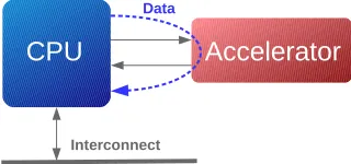
Remote Procedure Call
Another way to integrate hardware accelerators is by means of a Remote Pro-cedure Call (RPC). With a RPC the programmer has the ability to execute an instruction or a set of instructions at another place in the system. This tech-nique is depicted in Figure 2.2, where the CPU and hardware accelerator are both connected to the same interconnect.
Figure 2.2: Hardware Accelerator integration using a Remote Procedure Call
An example of integrating hardware accelerators by means of a RPC is the ST33F1M CPU developed by STMicroelectronics [24], targeting the domain of security applications (e.g. Pay TV, banking and transit). The micro-processor is based on a Cortex M3 CPU, where several external hardware modules have been added to a local bus. Examples of these modules are a Cyclic Redundancy Check (CRC) module, a Random Number Generator (RNG) and a coprocessor called Nescrypt which is used to execute specific security operations.
Stream Processing Hardware Accelerators
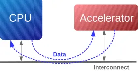
While there are clear differences between integrating hardware accelerators by means of an ISE or RPC, there are some similarities. One of them is the fact that in both cases the issuing CPU is also the CPU to which data has to be returned. Returning data to the same CPU is often not an optimized method for streaming applications. The best way to deal with the data resulting from an operation is send it away to another CPU. This way the issuing CPU can already start working on the next block of data, without having to care about the returning data. Adding hardware accelerators in a stream is a method optimized for streaming applications. This method is depicted in Figure 2.3. Not having to return data back to the issuing processor has an additional advantage; it opens the door of chaining multiple hardware accelerators together, which is also displayed in this figure. In [16] support for hardware accelerators was added to the Starburst platform, where the accelerators have been added in a stream.
Figure 2.3: Stream processing hardware accelerators
Not having to wait on the data to be returned, means that the issuing CPU can start working on the next packet of data. This follows the concept of SDF models. In these models each task can be mapped on either a CPU or hardware accelerator, constructing a stream of tasks. Furthermore, if the connection between the CPU and hardware accelerator has enough buffering capacity, this interconnect does not have any influence on the utilization of the issuing CPU. When the hardware accelerators and CPUs are connected to the same shared interconnect, this again opens the door to share the hardware accelerators across multiple CPUs.
2.2
Real-time analysis models
Real-time analysis techniques are used to guarantee the correct real-time be-haviour of a system. In this section three main analysis techniques will be discussed.
Event Models
Event Models (EM) [15] is the underlying analysis technique in the SymTA/S approach. This technique uses propagation of traffic, by characterizing the traffic with a period𝑃 and a jitter𝐽. Jitter is the maximum deviation between the arrival time of the k-th event, relative to the k-th period. The method is not suitable for cyclic graphs, where the addition of a feedback loop will result in an infinitely large jitter [2]. Furthermore, this technique can result in a low accuracy because it does not capture the correlation between different streams accurately [14]. This is because the correlation is captured in the time interval domain, which may result in a pessimistic characterization.
Real-time Calculus
Real-time Calculus (RTC) [11] is an analysis technique originating from the Network Calculus domain. It is also based on the characterization of traffic between components, however the correlation between streams is captured in the time domain, instead of the time interval domain. It has been shown that the Event Models technique is a special case of what can be represented with RTC.
A few years ago, this technique has been showed to be applicable for applications modelled as cyclic Homogeneous Synchronous Dataflow (HSDF) graphs [25]. However, it cannot handle a combination of cyclic resource dependencies and data dependencies [14].
Synchronous Dataflow
Maximum Cycle Mean (MCM) analysis. These techniques can be used to anal-yse temporal properties (e.g. deadlock freedom) or resource requirements (e.g. buffer sizes) for a practical implementation of the model.
2.3
Arbitration
In an MPSoC streams of data are processed by tasks, running on the processing elements of the MPSoC. In order to reduce costs, resources are being shared among these tasks, e.g. running multiple tasks on a single processor, letting multiple tasks share a single memory port or sharing the links of an NoC. Arbi-tration is the key ingredient to share these resources while guaranteeing temporal constraints such as throughput and latency constraints. The same holds when multiplexing multiple data streams over a single hardware accelerator. In order to guarantee temporal constraints, some form of arbitration is required. Fur-thermore, we want to be able to capture the effects of sharing such a resource in an SDF model. This chapter will focus on arbitration methods which can be captured in an SDF model.
Offline/online scheduling
One specific form of resource sharing is executing multiple tasks on a single CPU, where the CPU itself is a shared resource. In order to be able to meet temporal constraints, a designer has usually two options in a real-time system: calculating an offline schedule or using a run-time scheduler belonging to a specific class of schedulers. Scheduling at run-time instead of determining a fixed schedule at compile time is attractive for e.g. the following reasons [29]:
1. A high resource utilization can be obtained even in cases where there are tasks with a significant variation in their execution time and/or execution rate.
2. There is no need to compute and store a schedule for each combination of jobs that is simultaneously active.
3. Executing an arbitrary combination of tasks is simplified.
(Non-)Starvation free scheduling
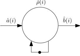
comes from the Network Calculus domain, where the effects of scheduling traffic passing through routers in a packet-switched network is captured in a simple and elegant model. The theory of this approach is based on a busy period of a session. A server belongs to the class of ℒℛ servers if the average rate of service offered during a busy session, over every interval starting at time Θ from the beginning of the busy period, is at least equal to its reserved rate 𝜌. The parameter Θ is called thelatency of the scheduler.
The next example is taken from [2] and will show how the effects of a TDM scheduler can be captured in a dataflow model. Figure 2.4 gives a schematic overview of a TDM scheduler. The scheduler can be modelled by a large rotating wheel where a task𝑎(𝑖) has a time-slice𝐵 in a total period𝑃. When the time-slice𝐵is depleted, the task is pre-empted. Only when a new period𝑃 is started, the task will get a new time-slice.
𝑎(𝑖) FIFO 𝑏(𝑖) FIFO P
B
Figure 2.4: Task scheduled under TDM with a fixed budget B (in red) during a period P (in blue)
ˆ
𝑎(𝑖) ˆ𝑏(𝑖) ˆ
𝜌(𝑖)
Figure 2.5: Single actor dataflow model
Figure 2.5 shows a single actor SDF-model. The idea is that the effects of scheduling a task under TDM is captured in the execution time ˆ𝜌(𝑖). The first step is determining the total execution time 𝜌(𝑗), which is the time between the arrival time of a task on edge 𝑎(𝑖) and the time at which the processor has finished processing this task. Figure 2.6 shows this principle. The total execution time𝜌(𝑗) is determined by the original execution time 𝑥(𝑗), plus the total time at which task 𝑎(𝑖) is not being serviced, which is equal to 𝑃 −𝐵, multiplied with the maximum number of pre-emptions task𝑎(𝑖) can encounter, which is equal to ⌈𝑥(𝑗)
happens when task 𝑎(𝑖) arrives just as budget𝐵 has been depleted. Therefore the ceiling function is used in this equation.
𝑃
𝐵
𝜌(𝑗)≤𝑥(𝑗) + (𝑃−𝐵)⌈𝑥𝐵(𝑗)⌉
Figure 2.6: Execution of a task during its time slices
The next step is proving that the dataflow model in Figure 2.5 is a valid
abstraction of the TDM scheduler in Figure 2.4. An abstraction is valid if the
arrival times of tokens on the edges of the SDF-model in Figure 2.5 are not earlier than the arrival times on the edges of the model in Figure 2.4, which corresponds to∀𝑖≥0,(∀𝑗, 𝑎(𝑗)≤ˆ𝑎(𝑗))⇒𝑏(𝑖)≤ˆ𝑏(𝑖).While the prove is beyond the scope of this example, mathematical induction can be used for this prove.
In [14] it is shown that also the effects of non-starvation free schedulers such as
Static Priority Pre-emptive scheduling can be modelled in a dataflow graph. For
a certain task𝜏𝑖the maximum amount of time it takes to execute𝑞consecutive executions is calculated (denoted by𝑤𝑖(𝑞)), by including the computation time of the set of tasks ℎ𝑝(𝑖) with a higher priority running on the same processor. It requires iterative fixed-point computation to calculate the response time, and therefore no closed-form expression for the throughput like MCM exists. This method requires, next to the execution times of all the tasks, knowledge about the arrival rates of these tasks.
2.4
State of the Art
This chapter will focus on related work considering the sharing of hardware accelerators in an MPSoC.
In [8] the difference between equipping all CPUs in the system with a dedicated (tightly connected) hardware accelerator and sharing a hardware accelerator on a globally shared On-chip Peripheral Bus (OPB) is investigated, by mapping an image compression algorithm on the system. The architecture uses a centralized Synchronization Engine which offers locks and barriers to the CPUs. When a CPU locks the shared accelerator, all subsequent requests will be queued and handled at a later stage. Interrupts are used to inform the requesting accelerator the computation is finished.
ap-Arbitration is the key ingredient when guaranteeing temporal constraints while sharing resources. This section focussed on capturing arbitration effects in a dataflow model. When a scheduler belongs to the class of ℒℛ-servers (like Round-Robin or TDM), it can be modelled with an SDF-graph. In contrast to Static Priority Pre-emptive scheduling, no fixed point computation is required to calculate the total waiting time.
Chapter 3
Starburst Platform
Chapter 1 gave an introduction to the research platform, this chapter will discuss the platform in more detail.
The Starburst hardware/software MPSoC platform is currently being developed within the University of Twente. The main goal for this project is to research and exploit: [1]
1. MPSoC architectures with means for low power, composability, and re-configurability.
2. A design flow for MPSoC based systems using high level synthesis.
3. An MPSoC run-time system management. By means of dynamic recon-figuration, the run-time system is capable of dealing with adaptive service requirements and platform variability.
The platform can be divided in three parts. The first part is the physical hardware platform which will be discussed in Section 3.1. Section 3.2 will focus on the reconfigurable hardware, such as the processing tiles, communication network and hardware accelerators. Section 3.3 covers the software layer running on the Starburst platform.
3.1
Hardware Platform
Figure 3.1: ML605 development board
3.2
Starburst
Figure 3.2 depicts a high level overview of the Starburst platform. In this figure the 32-core configuration is displayed, which is (given the available resources of the FPGA) currently the configuration with the maximum number of cores. In this figure different classes of components can be identified. The platform con-sists of a power-of-two processing tiles, a Linux tile dedicated to I/O capabilities (both depicted in blue), the Nebula ring network for all-to-all communication between the processing tiles and an arbitration tree to access DDR3 memory and several shared peripherals (both depicted in green). The components are red are peripherals available on the Starburst platform.
Figure 3.2: High level overview of the Starburst platform. Arrows indicate master-slave relations.
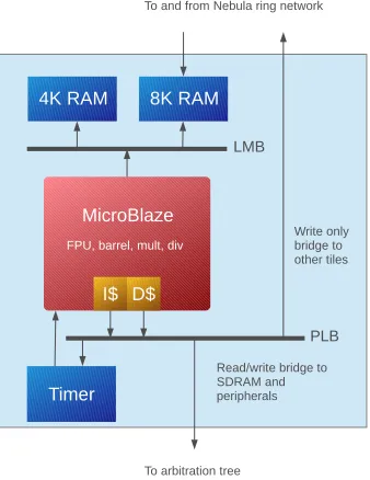
3.2.1
Processing tile
The basis of the Starburst platform is formed by the processing tiles, which are based on Xilinx MicroBlaze CPUs. Figure 3.3 gives an overview of a processing tile. The different components in this figure are discussed below.
The Xilinx MicroBlaze CPU is a Reduced Instruction Set Computer (RISC), organized as a Harvard architecture. This means that the CPU has separate bus interfaces for data and instruction access [37]. The Xilinx MicroBlaze is a so-called softcore which can be fully implemented in reconfigurable hardware by the logic synthesis tools. Due to this reconfigurability it is possible to configure the CPU at design time, where different components like a FPU, barrel shifter, hardware multiplier or hardware divider may be added to the CPU.
The MicroBlaze CPU is equipped with two caches; one instruction cache and one data cache. The caches are implemented without cache coherency between the processing tiles, there is only a write-back policy active. The size of these caches is configurable at design time, by default (and throughout this report) it has a size of 32 kB. When small streaming applications are executed, all instructions should fit into the instruction cache, which greatly reduces the number of requests to the shared memory.
Figure 3.3: Processing tile
memory is connected using a single cycle Local Memory Bus (LMB), and used for local data storage. This memory is also used for local kernel administration, e.g. cache sizes and the number of processing tiles in the system. Scratchpad Memory (SPM) is connected via the same LMB. This SPM is used for all-to-all communication between the processing tiles instead of using the shared memory for this purpose. This communication protocol will be discussed in Section 3.3.2.
TDM is used to implement multi-threading on the processing tile. For this purpose, and in order to keep track of time, a dedicated hardware timer is added to each processing tile.
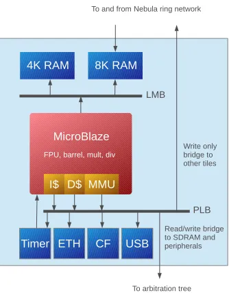
3.2.2
Linux tile
The Starburst platform contains exactly one Linux tile, which is almost an exact copy of a regular processing tile. The only hardware extension to the Xilinx MicroBlaze is the addition of a Memory Management Unit (MMU), which is necessary to be able to run Linux. The Linux tile is mainly used for I/O purposes, e.g. to communicate with the host PC, or control USB connected peripherals.
Figure 3.4: Linux tile
(CF) card, an the controller for the USB port.
3.2.3
Warpfield
The processing tiles and the Linux tile are connected to an interconnect which facilitates communication on the platform. The interconnect consists of two separate parts. The first part is the Warpfield arbitration tree. The arbitration tree is mainly used to access the DDR3 memory, but other components like the DVI controller and UART interface are also accessible through this interconnect.
The arbitration tree is developed to solve two traditional problems: super-linear scaling of hardware resources to the number of cores and a high latency for memory reads [23]. In order to overcome these problems an arbitration tree has been developed with the following features:
1. Starvation-free scheduling.
2. Work-conserving to optimize for latency.
3. Scales linearly in hardware costs to the number of cores.
4. Pipelined and decentralized arbitration to avoid long wires for high per-formance.
pack-etized and is given a timestamp and source ID. The packets enter a binary tree where at each step local arbitration based on the timestamp is applied. This way arbitration is applied according to a First-come, First-served (FCFS) policy, where a packet with the lowest timestamp is allowed to proceed first.
The last step is a demultiplexer, which routes the data to the correct peripheral. An additional demultiplexer is used to send data coming from the peripherals back to the corresponding Microblaze based on the source ID, without the need for any arbitration.
3.2.4
Nebula ring
The second part of the Starburst interconnect is the Nebula ring interconnect. This part of the interconnect provides an all-to-all communication network as a latency-tolerant interprocess channel. This in contrast to the Warpfield arbitra-tion tree, which is a latency-critical channel. In the latter type of channel, the performance degrades immediately with a higher latency. In the case of latency-tolerant channels this degradation depends on the application [23]. The Nebula ring interconnect has a small area footprint compared to other ring topologies. This small area footprint was achieved by: [13]
1. Making the Nebula ring unidirectional, which makes routing decisions triv-ial.
2. Under the assumption that slaves always accept data, FIFO buffers at the output of the network are omitted.
3. There is no need for FIFO buffers in the routers, because no contention or head-of-line blocking can occur.
4. There is no support for back-pressure. When a packet has entered the ring, it will travel one hop every cycle until it reaches its destination.
5. The ring provides automatic serialization, therefore no arbitration is re-quired when multiple masters want to write to the same slave.
Figure 3.5 gives a schematic overview of the Nebula ring NoC. In this schematic we can identify typical NoC components like routers and NIs. Every processing tile is connected via a NI to a router, and by connecting every router to its two neighbouring routers, a ring-like structure is created. The NIs form the bridges between the (network unaware) processing tiles and the networking part of the NoC.
Figure 3.5: Schematic overview of the Nebula ring
the connected NI. This action frees the occupied slot, so it can later be used to transfer a new data packet.
This construction, however, introduces starvation. If a processing tile would occupy all free slots, other processing tiles might never get access to send their data packets. To guarantee a processing tile access to the ring (and therefore eliminating starvation) a fairness protocol is implemented. All slots on the ring are labelled and a processing tile is only allowed to use a slot, when the slot-label equals the ID of the processing tile. This way all processing tiles are guaranteed to have an equal share of the total bandwidth. This traffic is classified as Guaranteed Service (GS) traffic.
The drawback of this fairness protocol is the fact that a lot of empty slots cannot be used by other processing tiles, reducing the available bandwidth of the ring interconnect. A work-conserving principle is introduced, by allowing slots to be hijacked under very strict conditions. The idea is that when an empty slot passes a router, this router may hijack this slot if the destination router is reached before the owner of the slot is reached. An overview of the rule set as implemented in the Nebula ring router, is given in Table 3.1. This traffic is classified as Best Effort (BE) traffic.
3.2.5
Hardware Accelerator integration
Figure 3.6: Schematic overview of two processing tiles and one hardware accel-erator, connected to the Nebula ring interconnect
possibility to easily chain multiple accelerators by letting one accelerator for-ward its data to a second accelerator and letting this second accelerator sending its credits back to the first one.
The last step is to return from the flow-controlled stream of data to a mem-ory mapped processing tile. Simply writing to the SPM of a processing tile is not supported, due to the absence of any form of flow-control. Furthermore, a hardware accelerator is only able to send data to a fixed address, where the SPMs have to be addressed consecutively. The ideal situation is to be able to emulate the software based FIFO communication (See Chapter 3.3.2), which is used to communicate data between processing tiles. The author from [16] determined this is not a trivial hardware design, and therefore came up with a temporary solution, where a hardware based FIFO buffer is directly connected to a MicroBlaze using a Fast Simplex Link (FSL). The FSL is an extension to the MicroBlaze execution pipeline, with an unidirectional point to point com-munication interface. With this construction a hardware accelerator is writing data in this hardware FIFO buffer, the consuming MicroBlaze will poll this buffer over the FSL interface to check whether new data is available. Figure 3.7 gives a complete overview of the integration of hardware accelerators including the ringshells and a FSL-link.
3.3
Software
Figure 3.7: Schematic overview of two processing tiles and one hardware accel-erator, connected to the Nebula ring interconnect.
hardware.
3.3.1
Helix kernel
Every processing tile in the system runs a small Portable Operating System Interface (POSIX) compatible operating system. This kernel has support for the newlib C library and implements multi-threading based on the Pthread standard. A TDM scheduler is implemented to switch between the threads on a processing tile. For this reason every processing tile is equipped with a dedicated hardware timer, which is the only interrupt source on a processing tile.
The Helix kernel runs several deamons for services like memory management, communication, synchronization, profiling, statistics and scheduling.
3.3.2
CFIFO
One service which deserves special attention is the service which offers commu-nication on the Starburst platform. One specific (and most frequently used) communication protocol is the software based C-HEAP FIFO (CFIFO) [22] im-plementation. With this implementation core-to-core communication can be set up for arbitrary data-types, with a configurable FIFO-depth and block-size.
version of the original pointer, and give therefore a conservative estimation of the amount of free or occupied positions in the software FIFO.
Figure 3.8: CFIFO administration overview
Chapter 4
System Architecture
This chapter will focus on a solution for our problem, by discussing several architectural alternatives.
4.1
Architectural Alternatives
While multiple system architectures were considered during this research, two basic principles can be identified. As an example Figure 4.1 illustrates the internals of an accelerator, where a set of arbitrary hardware operations are connected in a pipeline. Data enters the accelerator on the left side, and leaves the systems after it is being processed at the right side. Registers (𝑟𝑒𝑔0, 𝑟𝑒𝑔1)
are placed in between the operations, and store the intermediate results. Some operations may require a certain configuration, which is stored in an additional register (𝑐𝑜𝑛𝑓1).
OP0
data in data out
OP1 OP2
reg0 reg1
conf1
Figure 4.1: Hardware Accelerator pipeline
A problem arises when data samples from multiple data streams enter this system. The state and configuration registers can only store the contents for one data stream, mixing of data streams is simply not allowed. There are two basic solutions for this problem.
The first solution is based on the duplication of registers, which is displayed in Figure 4.2. In this image, the original pipeline is modified, were each register is replaced by a set of registers. Multiplexers and demultiplexer are used to select the correct register, based on the incoming data stream. In this example the registers are duplicated to support three data streams.
slots of the accelerator are occupied.
Another option is a more distributed solution, where the processors (who are sharing the same hardware accelerator) are required to program the accelerator, feed it with data and save the state afterwards themselves. When a processor is done, it informs the next processor that it can safely start using the accelerator. A clear advantage is the fact that this sharing mechanism could be implemented completely in software, an thus no additional hardware is required. A disad-vantage of this approach is the fact that this will not improve the utilization of the accelerators, as the low-speed data streams coming from the processors are processed in a sequential order.
The last option is a centralized solution, which is based around components which we callgateways. This idea is depicted in Figure 4.3. As discussed, the processors of the Starburst MPSoC are not able to read and write data fast enough over their local PLB. As a result, the utilization of the hardware ac-celerators remains relatively low. A gateway component (GW0) will temporary save the incoming low-speed data streams, and pushes the streams one at a time at high speed through the hardware accelerators. A second gateway (GW1) is used to route the data stream to the correct receivers.
Figure 4.3: Hardware Accelerator sharing via gateways
The centralized solution turned out to be best solution for our problem; addi-tional hardware is required but is has to be implemented only once, the uti-lization of the hardware accelerators is improved by streaming data streams at high speed over the hardware accelerators and depending on the application it is likely that this solution will also work when the application is mapped on hardware accelerators only.
4.3
Accelerator Gateway
4.3.1
Arbitration
When designing a method which implements hardware accelerator sharing, the most important requirement of this method is the fact that it should be pre-dictable. As discussed predictability is the ability to construct a sufficiently accurate temporal analysis model of the hardware design for which a compu-tational efficient analysis algorithm exists. With this model calculations can be performed and useful numbers (e.g. minimum throughput and maximum latency) can be extracted.
Section 2.2 focussed on different predictable scheduling techniques. As discussed in this chapter, it is possible to capture the effects of run-time scheduling in a dataflow model, if the scheduler belongs to the class ofℒℛ-servers. Examples of such schedulers are TDM and Round-Robin schedulers.
Furthermore, the scheduler is required to benon-preemptive. Preemption is the operation of suspending a running task, where the execution is resumed at a later moment in time [10]. On a CPU this technique is implemented in the operating system, and can for example be used to make sure that all tasks running on a CPU get some amount of processing time. The need for a non-preemptive scheduler can best be explained with an example. Figure 4.4 gives a schematic overview of a gateway, a hardware accelerator and a consumer. The orange arrow indicates the stream of data through the routers, NIs and the hardware accelerator. Actual data is depicted by the blue tokens on these arrows.
Figure 4.4: Non-preemption example: a gateway and a consumer are communi-cating data via a Hardware Accelerator
2. Data packets have to be buffered before they can be processed. In that sense, one should minimize the size of the data packets, as this allows smaller buffer sizes. With smaller buffer sizes, less memory has to be added to the system. Furthermore the latency introduced by the sharing mechanism is minimized.
The calculation of proper buffer sizes is a trade-off between maximizing the throughput over the accelerators and minimizing memory usage. This calcula-tion will be discussed as future work in Seccalcula-tion 8.2.
4.4
Summary
Chapter 5
Implementation
The previous chapter gave an overview of the system architecture. As explained a centralized gateway module will be implemented, which will take care of buffer-ing incombuffer-ing data streams and performbuffer-ing arbitration between the streams. This chapter will focus on the implementation of this module.
5.1
Hardware
A wide variety of tasks has to be supported by the gateway, such as:
∙ Buffering of incoming data streams.
∙ Reconfiguring of hardware accelerators.
∙ Performing arbitration over the data streams.
∙ Checking for free space at the output.
∙ Pushing data streams at high speed through the accelerators.
One question directly popped up during the design of this gateway; should the gateway be implemented in software, running on one of the processors in the system, should it be implemented completely in hardware, or is a combination of both worlds the best trade-off. When answering this question, one has to con-sider flexibility, hardware costs and power efficiency. Eventually the decision was made to start with a solution completely in software, running on one of the processors in the system. The idea behind this choice was to quickly implement a sharing mechanism in software, and then gradually replace parts of this (slow) software solution with a more efficient implementation in hardware. One of the advantages of using a CPU to implement accelerator sharing is the fact that communication between processors and the gateway module is already imple-mented, as the existing C-HEAP FIFO (CFIFO) protocol (see Section 3.3.2) can be used for this purpose.
Figure 5.1: Accelerator Interface
and the ringshell of a NI. The ringshell is the modular addition to the NI which implements for example credit based communication. The ringshell was modi-fied where a port was added to let it connect to the Accelerator Interface and logic was added to read and write state and configuration via this interface. By adding the required hardware to this modular extension, there was no need to modify each hardware accelerator separately.
Figure 5.4: Gateway overview, including DMA Controller
memory, but the DMA-controller still has to use single word transactions to forward its data to a NI. As no improvement in throughput is expected this way, two possible solutions for this problem are identified:
1. Modify the NI to support burst transactions.
2. Modify the DMA-controller to directly connect it to a NI, this way com-pletely bypassing the PLB.
Within the Starburst project, a hardware module was already being developed which incorporated a custom written DMA-controller in order to stream data from external memory at high speed over the Nebula ring interconnect and vice versa. This module can be used for benchmarking or debugging purposes. The decision was made to reuse parts of this component in order to make a DMA-controller which directly connected to the ring interconnect. Compared to the Xilinx DMA IP-core a lower area footprint was expected, as less functionality is required (more on this in section Section 7.1).
Figure 5.5: Schematic overview of the RingDMA controller
Figure 5.6 gives a new overview of the gateway module with this custom written DMA-controller incorporated. As depicted the DMA-controller is connected to a dedicated NI and router. Even though the additional NI will result in a higher area footprint, there are preliminary ideas to place the hardware accelerators on a dedicated interconnect which requires an additional NI in the first place. This idea will be discussed in more detail as future work in Section 8.2.
Figure 5.6: Gateway overview, including custom DMA Controller
Figure 5.9: Hardware Accelerator sharing overview, including exit gateway
0x18) has to be programmed and the word counter has to be set to zero (at address 0x1C).
After programming the Exit Gateway, the earlier discussed DMA controller can start streaming data. However, instead of polling the DMA controller to check if all data has been processed, the gateway should poll the Exit Gateway (at address 0x10) to determine if the programmed number of words have passed this component. This is still a sub-optimal solution, where additional traffic is gen-erated over the PLB limiting the achievable throughput of the DMA controller. Just as the DMA controller a solution based on interrupts is preferred but not yet implemented. A solution based on interrupts can therefore be considered as future work.
0 1 31
Credit Return Address 0x00 (Ringshell)
Data Forward Address (unused) 0x04 (Ringshell)
Data Snoop Address (unused) 0x08 (Ringshell)
Number of Credits (unused) 0x0C (Ringshell)
Unused Done
R 0x10 - Status register
Start Address 0x14
Packet Size 0x18
Word Counter 0x1C
Acclist class is able to determine if a requested accelerator is present, available and at which address the accelerator can be found. Right after creating the linked list, the programmer has to call the functionsetupStream(). This function will be recursively called by the accelerator objects in order to determine the availability and physical address for all accelerators in the linked list.
Chapter 6
Dataflow analysis
The previous chapter focussed on the implementation of the sharing mechanism. In this chapter we present the temporal analysis model. We start with a model where just one stream is being serviced by a gateway, next this model is extended to incorporate multiple streams.
6.1
Introduction
A dataflow model is a directed graph 𝐺𝑆(𝐸, 𝑉), consisting of actors 𝑣 ∈ 𝑉 and edges𝑒∈𝐸, where each edge describes a directed channel between actors:
𝑒𝑖= (𝑣𝑖, 𝑣𝑗). Edges represent unbounded queues to store tokens. Actors have a firing rule; when at least a specific number of tokens (called quanta) is present at all input edges the actor fires. When this happens all tokens at the input edges are instantly consumed, and after a certain execution time a specific number of tokens is produced at the output edges. When enough tokens are available an actor can fire multiple times simultaneously. Self edges with one token can be added to an actor in order to prevent parallel execution when this is not desired.
A large number of dataflow models exists, with different types of firing rules. In this chapter the following tree dataflow models are used: HSDF, SDF and CSDF. These models are visualized in Figure 6.1, and will now shortly be discussed.
v
01 1
v
02 3
v
0<2,1> <1,4>
HSDF
SDF
CSDF
Figure 6.1: Visualization of a number of dataflow models
This in contrast to SDF where an arbitrary number of tokens are consumed and produced. CSDF [5] extends SDF by introducing the concept of phases. Each actors cycles through a predefined number of phases, where 𝜌𝑣(𝑝) is de-noting the execution time for phase 𝑝. 𝜋(𝑒𝑖𝑗, 𝑝) and 𝛾(𝑒𝑖𝑗, 𝑝) are respectively denoting the production quanta and consumption quanta on edge 𝑒𝑖𝑗 during phase 𝑝. Furthermore, the number of phases for actor 𝑣𝑖 is denoted as 𝜃(𝑣𝑖). It is important to note that all actors do not need to have the same number of phases. Overlapping firings are not allowed [5], which means that all actors have an implicit self-edge with a single token on it. One exception to this rule are single-phase actors, we allow them to fire concurrently. Self-edges have to be added to prevent overlapping firings.
Two important properties are being used in this discussion; refinement and
abstraction[2]. A component is said to refine another component in the temporal
domain if:
∀𝑖, 𝑚 ∙ 𝑎ˆ′𝑚(𝑖)≤ˆ𝑎𝑚(𝑖)⇒ ∀𝑗, 𝑛 ∙ 𝑏ˆ′𝑛(𝑗)≤ˆ𝑏𝑛(𝑗) (6.1)
Where𝑎𝑚are the input ports and𝑏𝑚the output ports of component𝐶, and𝑎′𝑚 the input ports and𝑏′
𝑚the output ports of component𝐶′. In other words, this implies that one component𝐶′ refines a component𝐶, then in the worst-case situation tokens produced by 𝐶 do not arrive earlier than tokens produced by
𝐶′. Refinement is denoted as𝐶′⊑𝐶. The opposite of refinement is abstraction. Abstraction is most of the time used to reduce the number of cases that need to be considered during analysis, this comes however at a cost of a reduced accuracy.
6.2
Nebula Ring Network
An important property of the Nebula ring network is the fact that it can be modelled with a dataflow model. There are two types of traffic on the Neb-ula ring network (CFIFO communication and credit-based communication), the dataflow models of both communication protocols will be discussed in the next sections.
6.2.1
CFIFO Communication
occurs when a packet with a size of 𝑆 has to be communicated, where𝑆 > 𝛼. In that situation the model will deadlock as none of actors is able to fire.
P
Acc
1 1
ˆ
ρ
Pρ
ˆ
Accα
S 1
1 S
Figure 6.3: Potentially dead-locked accelerator communication model
Figure 6.4 shows an CSDF model of the accelerator communication model. A packet of𝑆 words is communicated in𝑆separate phases, where single words are written at the end of each phase. After word has been accepted by accelerator
𝐴𝑐𝑐, a credit is sent back to the consumer. In contrast to the previous model, this model is dead-lock free if𝛼 < 𝑆.
P
Acc
1< ρP(0), ..., ρP(S−1)> < ρAcc(0)>
α
< S×1> <1>
<1> < S×1> <1>
<1>
Figure 6.4: CSDF accelerator communication model
Figure 6.5 depicts the same CSDF model, where the earlier discussed latency and rate actors have been added. In contrast to the CFIFO communication pro-tocol, credits are travelling on a dedicated credit-ring, rotating in the opposite direction. This has consequences for the latency actor 𝐿𝐶, as the credits have to travel the same distance (𝐷−1) as the actual data.
6.3
Single data stream
actors to force a graph to execute with a certain period⋆ 𝑇. The schedule is then called a Static Periodic Schedule (SPS) and is defined as:
𝑠(𝑣, 𝑘) =𝑠(𝑣,0) +𝑇.𝑘 (6.6)
In [21] it is proven that for any HSDF graph G, it is possible to find a SPS schedule as long 𝑇 ≥ 𝜇(𝐺). If 𝑇 < 𝜇(𝐺) no SPS exists. If the period T is chosen such that it is equal to the MCM 𝜇(𝐺), the schedule is called a Rate Optimal Static Periodic Schedule (ROSPS):
𝑠(𝑣, 𝑘) =𝑠(𝑣,0) +𝜇(𝐺).𝑘 (6.7)
Concluding, when worst-case execution times are assumed during the self-timed execution of graph G, the graph will fire according to the WCSTS. Eventually (after a transition phase 𝐾) the schedule will settle into a periodic behaviour, with a period𝜇(𝐺). On the other hand it is always possible to enforce a graph
𝐺to execute with a period𝑇 ≥𝜇(𝐺). When𝑇 =𝜇(𝐺) the schedule is called a ROSPS. It is important to note that because of monotonicity in any admissible SPS schedule actors can never fire earlier than the WCSTS. This way you can see an SPS as an upper bound; under the WCSTS actors will never fire later than this SPS.
6.3.5
Schedule Calculation
In the previous section we showed that the ROSPS schedule can be used as an upper-bound, as the actors of the corresponding graph 𝐺 will never fire later during self-timed execution. Via this periodic schedule we are able to give a parametric solution for the total processing time, which will be discussed in this section. In Figure 6.14 our constructed HSDF graph is displayed. What we are interested in, is the production time of the𝑆-th token on actor𝐺𝑊1, defined as
𝑓(𝐺𝑊1,(𝑆−1)) =𝑠(𝐺𝑊1,(𝑆−1)) + ˆ𝜌(𝐺𝑊1) (6.8)
As discussed in the previous section, it is sufficient to calculate this finishing time based on the ROSPS, during STS the firings will never happen later. From Equation 6.7 and Equation 6.8 it follows that
𝑓(𝐺𝑊1,(𝑆−1)) =𝑠(𝐺𝑊1,0) + (𝑆−1)·𝜇(𝐺) + ˆ𝜌(𝐺𝑊1) (6.9)
<