Available Online at www.ijcsmc.com
International Journal of Computer Science and Mobile Computing
A Monthly Journal of Computer Science and Information Technology
ISSN 2320–088X
IMPACT FACTOR: 5.258IJCSMC, Vol. 5, Issue. 5, May 2016, pg.720 – 725
Performance Analysis of an
Efficient Reconfigurable Multiplier
for Multirate Systems
Ms.P.P.Harde
1, R.V.Kshirsagar
2, A.C.Bhagali
3¹Electronics Engineering, DBACER, RTM Nagpur University, India ²Principal, PIGCOE, RTM Nagpur University, India
³Director, SBGI, Shivaji University, India
1
[email protected]; 2 [email protected]; 3 [email protected]
Abstract— This paper describes an efficient run-time architecture of a reconfigurable multiplier for digital signal processing applications using multirate systems. The advantages of the proposed architecture are (i) it can be easily reconfigured to trade bit width for array size, thus maximizing the utilization of available hardware and the high order of flexibility, which allows an easy configuration for different data bit widths (ii) the low hardware complexity, which results in small area and (iii) the low propagation delay, which results in faster speed. The novel multiplier multiply signed or unsigned data and uses part of its structure when needed. The proposed reconfigurable circuit consists of an array of m×m multipliers, adders, multiplexers, demultiplexers and registers. The circuit reconfiguration can be done dynamically through using only a few control bits. The architecture design of the reconfigurable multiplier, with hardware equivalent to one 64×64 bit high precision multiplier, which can be dynamically reconfigured to produce an array of the products in different forms is described in detailed manner.
Keywords—―Reconfigurable, multirate, multiplier, multiplexer, demultiplexer‖.
I. INTRODUCTION
applications in digital audio transmission, speech processing, telecommunications, wavelet transform, digital
filtering etc.
In many applications the sampling rate of the signal is converted into an equivalent signal with a different sampling rate. For example, in digital audio transmission, three different sampling rates are used: 32 kHz in broadcasting, 44.1 kHz in digital compact disc (CD), and 48 kHz in digital audio tape (DAT) (Fliedge, 2000;Mitra, 2001). Conversion of the sampling rate of audio signals between these three different rates is often necessary. For example, if we wish to play CD music which has a rate of 44.1 kHz in a studio which operates at a 48 kHz rate, then the CD data rate must be increased to 48 kHz using a multirate technique.
The rest of the paper is organized as follows: section II briefly describe about reconfigurable multiplier and its advantages, In Section III architecture design & Implementation is explained in brief. Section IV gives simulation result and the performance of the circuits. Finally, Section V concludes the paper discussing the analysis of the circuit based on the performance parameters.
II. RECONFIGURABLEMULTIPLIER
It has been suggested that FPGAs are best suited for use as reconfigurable hardware to accelerate software in many applications [1]. Image/video processing tasks are particularly uses hardware acceleration, because of the parallelism and data flow structure is common to many images and video processing tasks. For this it uses intensive arithmetic operations such as multiplication and addition. The existing FPGA architectures are well suited to binary addition, configuring FPGAs for binary multiplication results in the available reconfigurable resources being used inefficiently. Typically over 70% of the FPGA resources could be used only for multiplication in some applications. The literature also suggests that hardware implemented on an FPGA requires as much as 100 times more die area, and will be about 10 times slower than the custom hardware equivalent .This issue can be solved by embedding custom multipliers into the FPGA structure. The difficulty with this is that inefficiencies will result if the operand size of the multiplier is not compatible with that of the algorithm. We suggest that a better solution is to use FPGAs with reconfigurablemultiplier blocks for multirate digital signal processing applications. In this paper we suggest a design for a 8X8 reconfigurable multiplier. It consists of multiplexers, demultiplexers and registers which can be combined together to construct a multiplier which has speed comparable to that of a conventional signed array multiplier, with minimal extra cost in hardware required for reconfiguration. The multiplier can be configured to perform any 8 x 8 bit signed/unsigned binary multiplication.
III.DESIGNOFRECONFIGURABLEMULTIPLIER
The multiplication operation performs two major steps 1) performing partial products and 2) Accumulation of partial products to get final product.
Let us consider two 8 bit nos. A, A7---Ai---A0 and B, B7---Bj---B0.According to the basic equation for multiplication [3],
∑AiBj2i+j = ∑ ∑ AiBj2i+j
0≤i,j≤7 0≤m,n≤1 4m≤i≤3+4m (1) 4n≤j≤3+4n
Eq. (1) implies that an 8X8 multiplication is equivalent to four, 4X4 multiplications where m and n are integers A{0, 1}.We build partial products of 4X4 matrices, which are to compose an 8X8 partial product matrix The weighted bits of the four products of the four multipliers are added by two adders to result in the final product of the 8X8 multiplier.
The approach described above for decomposition of an 8×8 partial product matrix into four, 4×4 ones can be applied recursively for larger size inputs of such computations in multi rate digital signal processing applications.
The architecture of an 8X8 multiplier is shown in fig 1. The four products of the 4X4 multipliers pass through an array of demultiplexers controlled by the control 1 bit. When control1 is set low a Block 8X8 performs four 4X4 multiplication giving 8-bit products, while if control1 is „1‟ it performs 8X8 bit multiplication deriving a 16-bit product. The three operands 8-bit carry-save adder that consists of an array of full adders and half adders, and a ripple carry adder. We sought for a fast three-operand adder and we chose a carry-save adder, which, for multiple operands, is faster and more efficient in area coverage than a carry-look ahead adder . The two registers provide the ability to complete the 8X8 multiplication in two pipeline stages. The two multiplexers, controlled by control 2, can disable the registers thus reducing the pipeline stages.
stage or not.In this architecture we have the choice of multiplying less pairs of operands, i.e., only two pairs of operands, by setting the two out of the four Blocks in ideal state.
The smallest unit to perform multiplication is a 4X4 array multiplier. An array multiplier is the simple regular structure consists of few logic gates. In an array multiplier bit products generation & accumulation is done using identical cell array. All bit-products are generated in parallel and collected through an array of full adders and final adder. Demultiplexers performs the function of data distribution (product of four,4X4 multipliers) and also gives product of 4,4X4 multipliers individually.Multiplexer1 combine the output of demultiplexers depending on the status of control1 signal. Two adders, adder 1 perform 4+2 bit addition and adder2 performs 3,8-bit addition are used. Registers acts as the pipelining stage which can be disabled or enabled as per requirement.
32 bit data
4, 8 bit outputs 16 bit output
Fig.1 8X8 Reconfigurable Multiplier
Four,4 X 4 Multiplier
Demultiplexers
Adder 1
Adder 2
Multiplexer_1
32 bit- Registers
16 bit- Registers
Multiplexer_2
Control 1
Conrtrol 1
Control 2
Conrtrol 1
CLKIV.SIMULATIONRESULT
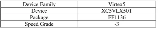
For experimental simulation of the multiplier, demultiplexers ,multiplexers and registers, the codes are written in VHDL (VHSIC Hardware Descriptive Language) and simulated using Xilinx ISE9.2i.
TABLE I SUMMARY OF FPGA
Device Family Virtex5 Device XC5VLX50T Package FF1136 Speed Grade -3
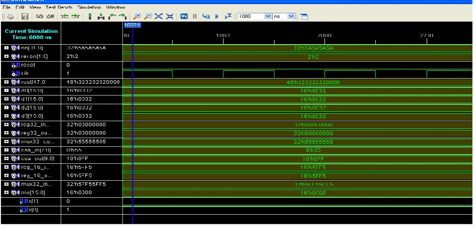
The multiplication of 4X4-bit numbers generates eight-bit product terms. The simulation results are as follows-
Fig. 2 Simulation result of 4X4 array multiplier
Fig. 4 Simulation result of 8X8 reconfigurable multiplier
TABLE III
DESIGNSUMMARY OF 8X8 RECONFIGURABLE MULTIPLIER
Total memory usage 139652 kilobytes IOB Utilization 84/480 =17.5 % FlipFlops/Latches 245/28800=0.8 %
Total Delay 5.58ns
V. CONCLUSIONS
In this paper we propose a reconfigurable multiplier circuit which can be used efficiently in multirate digital signal processing applications. Fast circuits are required to achieve parallel processing in digital system. Hence fast multiplier is required. An array multiplier has less delay than other multipliers. Hence it is used as a basic block. Reconfigurability in FPGA can be used to implement proposed design. It helps in reducing propagation delay, memory utilization and area consumption of the device.
R
EFERENCES[1] P.M. Athanas, and A.L. Abbott, “Real-time image processing on a custom computing platform”, IEEE
Computer,Vol. 28, No. 2 , pp. 16-24, 1995
[2] Altera Corporation. “Ripple-carry adders in FLEX 8000 devices”, Application Brief 118, ver. 2, May
1994
[3] G. Koutroumpezis, K. Tatas, D. Soudris, S. Blionas1, K. Masselos1, and A. Thanailakis “Architecture Design of a Reconfigurable Multiplier for Flexible Coarse-grain Implementations”
[4] Joshin Mathews Joseph & V.Sarada,” Reconfigurable High Performance Baugh-Wooley Multiplier for DSP Applications” ITSI Transactions on Electrical and Electronics Engineering (ITSI-TEEE) ISSN (PRINT) : 2320 – 8945, Volume -1, Issue -4, 2013
[5] S. C. Goldstein, H. Schmit, M. Budiu, S. Cadambi, M. Moe, and R.Taylor Architecture Design of a Reconfigurable Multiplier for Flexible Coarse-grain Implementations "PipeRench: A Reconfigurable Architecture and Compiler" in IEEE Computer, Vol.33, No. 4, April 2000.
[7] Ragavi.M1, Thilakavathi.S2, Raveena Shree.K3 , “ An efficient multiplier architecture design for fir filter ”, International Research Journal of Engineering and Technology (IRJET) e-ISSN: 2395-0056 Volume: 02 Issue: 08 | Nov-2015, p-ISSN: 2395-0072
[8] C.S. Wallace, “A suggestion for fast multipliers”, IEEE Trans. Electronic Computers, Vol. EC-13, pp.
14-17, Feb.1964