Basic Analog and Digital
Student Guide
WARRANTY
Parallax, Inc. warrants its products against defects in materials and workmanship for a period of 90 days. If you discover a defect, Parallax will, at its option, repair, replace, or refund the purchase price. Simply call for a Return Merchandise Authorization (RMA) number, write the number on the outside of the box and send it back to Parallax. Please include your name, telephone number, shipping address, and a description of the problem. We will return your product, or its replacement, using the same shipping method used to ship the product to Parallax.
14-DAY MONEY BACK GUARANTEE
If, within 14 days of having received your product, you find that it does not suit your needs, you may return it for a full refund. Parallax, Inc. will refund the purchase price of the product, excluding shipping / handling costs. This does not apply if the product has been altered or damaged.
COPYRIGHTS AND TRADEMARKS
This documentation is copyright 1999-2008 by Parallax Inc. By downloading or obtaining a printed copy of this documentation or software you agree that it is to be used exclusively with Parallax products. Any other uses are not permitted and may represent a violation of Parallax copyrights, legally punishable according to Federal copyright or intellectual property laws. Any duplication of this documentation for commercial uses is expressly prohibited by Parallax Inc. Duplication for educational use is permitted, subject to the following Conditions of Duplication: the text, or any portion thereof, may not be duplicated for commercial use; it may be duplicated only for educational purposes when used solely in conjunction with Parallax products, and the user may recover from the student only the cost of duplication.
This text is available in printed format from Parallax Inc. Because we print the text in volume, the consumer price is often less than typical retail duplication charges.
BASIC Stamp, Stamps in Class, Board of Education, Boe-Bot, SumoBot, Toddler, and SX-Key are registered trademarks of Parallax, Inc. HomeWork Board, Propeller, Parallax, and the Parallax logo are trademarks of Parallax Inc. If you decide to use trademarks of Parallax Inc. on your web page or in printed material, you must state that "(trademark) is a (registered) trademark of Parallax Inc.”, “upon the first appearance of the trademark name in each printed document or web page. Other brand and product names are trademarks or registered trademarks of their respective holders.
ISBN 10: 1-928982-04-2 ISBN 13: 9-781928-982456 1.4.0-08.05.13-SCP
DISCLAIMER OF LIABILITY
Parallax, Inc. is not responsible for special, incidental, or consequential damages resulting from any breach of warranty, or under any legal theory, including lost profits, downtime, goodwill, damage to or replacement of equipment or property, and any costs or recovering, reprogramming, or reproducing any data stored in or used with Parallax products. Parallax is also not responsible for any personal damage, including that to life and health, resulting from use of any of our products. You take full responsibility for your BASIC Stamp application, no matter how life-threatening it may be.
web site:
Propeller Chip – This forum is for users of the multiprocessing Parallax Propeller chip.
BASIC Stamp – This forum is widely utilized by engineers, hobbyists and students who share their BASIC Stamp projects and ask questions.
SX Microcontrollers and SX-Key – Discussion of programming the SX microcontroller with Parallax assembly language SX – Key® tools and 3rd party BASIC and C compilers.
Stamps in Class® – Created for educators and students, subscribers discuss the use of the Stamps in Class series in their courses. Students, educators and hobbyists are welcome to participate.
Javelin Stamp – Discussion of application and design using the Javelin Stamp, a Parallax module that is programmed using a subset of Sun Microsystems’ Java® programming language.
Robotics – Designed exclusively for Parallax robots, this forum is intended to be an open dialogue for robotics enthusiasts. Topics include assembly, source code, expansion, and manual updates. The Boe-Bot™, Toddler™, SumoBot®, HexCrawler and QuadCrawler robots are discussed here.
HYDRA – A place for enthusiasts of the Propeller-based HYDRA game development system.
Parallax Educators – A private forum exclusively for educators and those who contribute to the development of Stamps in Class. Parallax created this forum for educators to provide feed back and to obtain, develop, and share teaching materials.
ERRATA
While great effort is made to assure the accuracy of our texts, errors may still exist. If you find an error, please let us know by sending an email to [email protected]. We continually strive to improve all of our educational materials and documentation, and frequently revise our texts. Occasionally, an Errata sheet with a list of known errors and corrections for a given text will be posted to our web site, www.parallax.com. Please check the individual product page’s free downloads for an errata file.
Table of Contents
Preface...v
Audience and Teacher’s Guide ...v
Conditions of Duplication ... vi
Foreign Translations ... vi
Special Contributors ... vi
Chapter #1: Analog Voltage and Binary States ...1
Introduction to Analog and Digital...1
Parts Required ...2
Building the Analog and Digital Comparator ...7
Programming the Project ...9
What have I learned? ...15
Questions ...16
Challenge! ...16
Why did I learn it? ...17
How can I apply this? ...17
Chapter #2: Introduction to Bit Crunching ...19
Basic Comunication ...19
Parts Required ...19
Building the Circuit ...20
Programming the Project ...22
Parallel and Serial Transmission...30
Reprogramming to Receive Serial Data...31
What have I learned? ...37
Questions ...38
Challenge! ...38
Why did I learn it? ...39
How can I apply this? ...39
Chapter #3: Basic Analog to Digital Conversion...41
Build Your Own Digital DC Voltmeter ...41
Parts Required ...42
The Potentiometer - A Source of Variable Voltage ...42
The ADC0831 Integrated Circuit - An 8-bit Analog to Digital Converter ...43
Build It ...45
Program It ...45
Binary to Decimal Conversion Revisited ...52
Calculate Voltage ...54
Resolution ...61
What have I learned?...63
Questions...64
Challenge!...64
Why did I learn it? ...65
How can I apply this?...65
Chapter #4: Basic Digital to Analog Conversion ... 67
Build a Resistive Ladder Network...67
Parts Required ...68
Build It ...69
Program It ...70
Addressing ...76
The Voltage Follower ...81
What have I learned?...85
Questions...86
Challenge!...86
Why did I learn it? ...87
How can I apply this?...87
Chapter #5: Time Varying Signals... 89
Parts Required ...90
Program It ...91
The Pulse Train...97
The Sine Wave and Pulse Width Modulation (PWM) ...100
Reprogram the Circuit for Musical Notes ...102
What have I learned?...104
Questions...105
Challenge!...105
Why did I learn it? ...106
How can I apply this?...106
Chapter #6: Recording Frequency Data ... 107
Parts Required ...107
Build It ...108
The Output ...111
Program It ...114
What have I learned?...119
Questions...120
Challenge!...120
Why did I learn it? ...121
How can I apply this?...121
Chapter #7: Digital to Analog the Easy Way using PWM... 123
Build It ...127
Program It ...129
What have I learned? ...137
Questions ...138
Challenge! ...138
Why did I learn it? ...139
How can I apply this? ...139
Chapter #8: Light Meter Gizmo with R/C Time Constants...141
Parts Required ...144
Build It ...144
Program It ...146
Do the Math...150
What have I learned? ...152
Questions ...153
Challenge! ...153
Why did I learn it? ...154
How can I apply this? ...154
Appendix A: Parts Listing and Sources...157
Appendix B: Resistor Color Code...159
Preface
The personal computer brought in a whole new era of electronic sophistication. With it, we have immense amounts of digital computing power located right at our desk. Computers work well when they are connected to each other, and digital data can be transferred quite reliably from machine to machine.
However, the minute you wish to connect a digital computer to some “real world” device (such as a wind speed indicator or fuel level sensor) you need to design a circuit that interfaces an analog device to the digital computer. In many cases, this involves the conversion from an analog voltage to a digital representation of that voltage.
This set of Stamps in Class experiments will explore many of the basic principles of interfacing analog devices to digital microcontrollers. Many times this involves the use of easy-to-use commands built right into the BASIC Stamp, and at other times requires the use of a an “analog to digital converter”.
Why should we be interested in converting from analog to digital? Many different aspects of our lives are dependent upon this conversion process. Some are not too critical to our survival like compact disc players, telephone systems, and music. Others, however, might be critical. Medical equipment and sensors often require analog to digital and digital to analog conversion.
The Basic Analog and Digital text will be revised and updated continually based on feedback from students and educators. Version 1.4 was edited to change from a 100 kΩ to a 10 kΩ potentiometer due to supply issues. Additionally, program listings PL3_1R0.bs2 and PL4_1R0.bs2 were updated to accommodate modification for several ADC0831 chips connected to the same CLK (clock) and D0 (data) lines. Pagination remains similar if not identical to Version 1.3.
AUDIENCE AND TEACHERS GUIDE
The audience for this text is ages 17 and above. This guide can be used as a complete book to introduce analog and digital concepts in a class, or as a reference to obtain detailed explanations about hardware and techniques used in other Stamps in Class Student Guides.
The answers to these experiments present no impossible or very difficult technical hurdles, and could be solved with a bit of patience. Instructors could participate in an Educator’s Forum to obtain support or Teacher’s Guides if they are available.
CONDITIONS OF DUPLICATION
Parallax grants the user a conditional right to download, duplicate, and distribute this text without Parallax's permission. This right is based on the following conditions: the text, or any portion thereof, may not be duplicated for commercial use; it may be duplicated only for educational purposes when used solely in conjunction with Parallax products, and the user may recover from the student only the cost of duplication.
This text is available in printed format from Parallax, Inc. Because we print the text in volume, the consumer price is often less than typical retail duplication charges.
FOREIGN TRANSLATIONS
Parallax educational texts may be translated to other languages with our permission (e-mail [email protected]). If you plan on doing any translations please contact us so we can provide the correctly-formatted MS Word documents, images, etc. We also maintain a discussion group for Parallax translators which you may join. This will ensure that you are kept current on our frequent text revisions.
SPECIAL CONTRIBUTORS
Version 1.0 of this text was written mostly by Andy Lindsay based on a manuscript submitted by Matt Gilliland, original author of What's a Microcontroller? and the ever-popular Microcontroller Application Cookbooks. Andy wrote this text during his senior year at California State University, Sacramento, where he studied Electrical and Electronic Engineering. This was his first of many Stamps in Class texts that he has revised and/or authored. Andy is also is a contributing author of several papers that address the topic of microcontrollers in pre-engineering curricula. When he’s not writing educational material, Andy does product engineering for Parallax.
Chapter #1: Analog Voltage and Binary States
This series of experiments introduces analog and digital electronics. What does that mean? In What’s a Microcontroller? we learned that analog is a “continuously variable value”. Another way to think about it is that analog electronics is analogous to nature. There are lots of continuously variable values in nature, such as motion, light level, and sound. The position of a door as it swings open is a good example of a continuously variable value. As a door swings from all the way closed to all the way open, it visits every value in between. At one instant during its travel, it is 1/3 of the way open. At another instant, it is 1/2 way open, and so on.INTRODUCTION TO ANALOG AND DIGITAL
Digital simply means represented by digits. Think about how many times each day you encounter analog values that are represented with digits. The temperature is 79.8 degrees. The speed limit is 45 miles per hour, etc. Not surprisingly, digital electronics represents values with digits.
The term digital is also used when referring to binary devices such as the circuitry that makes a calculator work, the microprocessor in a computer, and the BASIC Stamp microcontroller. It's true - they are all digital devices. Binary devices are digital devices using two digits, 0 and 1.
The experiments in What’s a Microcontroller? introduced a variety of techniques for interfacing with the outside world and other devices. These interfaces were mostly binary. This series of experiments extends the capabilities of interfacing by introducing several analog component interfaces and more component interface techniques.
In this first experiment, we'll build a circuit that produces an analog voltage at its output. Remember that analog voltage is continuously variable. The circuit will be adjustable so that it can produce an output anywhere between 0 and 5 volts. We'll also build a circuit called a voltage follower that uses this analog voltage to drive an LED circuit.
Volt/Voltage: The volt is a fundamental unit of electrical measurement named after 18th century physicist Allesandro Volta, and a measurement in volts is referred to as voltage. Most of us encounter this unit of measurement when buying batteries such as the 9 volt (DC) battery that can be used to power the Board of Education or BASIC Stamp HomeWork Board. Inside a battery there are two chemical reactions, which are separated from each other by a barrier. One of the reactions creates a surplus or electrons and the other creates a shortage of them.
The electron surplus and shortage sides of the barrier are connected to the negative and positive terminals of the battery respectively. If given a pathway around the barrier, the electrons have the potential to do work to get from the negative to the positive terminal. The volt is a measure of this potential to do work. The volt is also referred to as a unit of electric potential.
The analog voltage will also be connected to one of the BASIC Stamp I/O pins set to input mode. This binary input can actually be used to measure small variations in the analog voltage. PBASIC will be used to program the BASIC Stamp to drive a binary LED circuit, which will indicate when these variations have been detected.
The Debug Terminal is also a useful tool for displaying data the BASIC Stamp collects and sends. It will be used to monitor the binary value that the input pin receives as the analog voltage is varied.
Parts Required
For each experiment you will need a BASIC Stamp 2 microcontroller module on a Board of Education platform or a BASIC Stamp HomeWork Board. Your board needs to be connected to an IBM-compatible PC with Windows 2K/XP/Vista. You will need to install the BASIC Stamp Editor v 2.4 or higher, which is available for free download from www.parallax.com. (If you are using a USB board or a Parallax USB to Serial Adapter, you will need the FTDI USB VCP driver software installed; it installs automatically with the BASIC Stamp Editor v 2.4 or higher.) In addition, you'll need the following parts for this experiment:
(2) 470 Ω resistors (2) Red LEDs
(1) 10 kΩ potentiometer (6) Jumper wires (1) LM358 op-amp
Flat spot on plastic part of LED indicating the cathode.
Throughout this series of experiments, we will build circuits from circuit schematics. One of the keys to learning how to read circuit schematics is learning what each symbol on the schematic means. It's also important to learn how to connect a part from the Analog and Digital Parts Kit to the prototyping area (also called a breadboard) of your Board of Education or HomeWork Board based on its circuit symbol in a schematic.
Circuit Schematic: Often referred to as a schematic, a circuit schematic is a map that uses symbols to show the components in a circuit and how they are connected. The components are represented by symbols such as the one that represents the LED in Figure 1-1.
Figure 1-1 shows the circuit symbol for an LED on the left and a drawing of an LED from the parts kit on the right. It also shows how the pins on an LED correspond to the terminals on the circuit symbol.
+ _
LED
Figure 1-1
LED Circuit Symbol Compared to the Component
Figure 1-2 shows a drawing of a resistor below its circuit symbol. The circuit symbol typically has the resistance value written below or next to it. The colored stripes on the part drawn below the symbol indicate its value, which is measured in ohms. The omega symbol (Ω) is used to denote the ohm. You can use Appendix B to convert the color codes on the resistor to resistance values.
470 Ω Figure 1-2 Resistor Circuit Symbol and Corresponding Component
Current/Amp: Current happens when electrons travel from point A to point B. Direct current is what happens when you give the surplus electrons in the negative terminal of a battery a pathway to get to the positive terminal. The amp is the measurement of how many electrons per second are traveling through the pathway.
Resistance/Ohm: Resistance is a property of a material in the pathway the electrons travel through. The more difficult it is for the electrons to get from one end of the pathway to the other, the higher the resistance. A resistor is just such a pathway, and its resistance is measured in ohms (Ω).
Ohm's Law: When a resistor is used to provide a pathway between the negative and positive terminals of a battery, you have an electric circuit with voltage, resistance, and current. Ohm's Law relates the three quantities as follows:
V = I x R
V is the voltage measured in volts, I is the current measured in amps, and R is the resistance measured in ohms.
The Other Guys: Ever wonder where the words volt, amp, and ohm come from? They are all named after some of the people who made significant discoveries about electricity. We already know who the volt is named for; what about the other guys? The amp, also called the ampere, is named after 18th century physicist André Marie Ampère. The ohm is named after 19th century physicist Georg Simon Ohm.
The Potentiometer - A Source of Variable Voltage
The potentiometer (pot) has 3 pins on its underside that get plugged into the breadboard. On the topside, it has a knob you can twist to adjust it. In this experiment, we will use variable resistance to get a variable voltage output. Figure 1-3 shows how the pins on the underside of the pot from the parts kit correspond to the circuit symbol.
Pot
Figure 1-3
Potentiometer Circuit Symbol and Component
Figure 1-4 shows what happens inside the pot as it is adjusted. The jagged line represents a resistive element, typically made of carbon. One end of the resistive element is wired to Vdd on your board, and the other end is wired to Vss. The middle of the three terminals is connected to the “wiper”, and it’s where the variable output voltage is measured. The wiper stays in contact with the carbon element as it moves.
As the wiper gets closer to Vdd, the voltage measured at the wiper terminal will approach the value of Vdd, which is 5 volts. Likewise, when the wiper is closer to Vss, the voltage at the wiper terminal will be closer to Vss, which is 0 volts. As the wiper terminal travels between Vdd and Vss, the output measured at the wiper terminal varies between these two values in a manner analogous to a door as it opens and closes.
Figure 1-4
Potentiometer Wiper Showing how the wiper in a potentiometer travels along the surface of the resistive element as it’s adjusted. The LM358 Op-amp
An op-amp (operational amplifier) is a building block commonly used in analog circuits. Figure 1-5 shows the circuit symbol and block diagram for the LM358 op-amp used in this experiment. The op-amp circuit used in this experiment is called a voltage follower because the same voltage comes out as goes in. In other words, the voltage at the output "follows" the voltage at the input. The reason it's used in the circuit in this experiment is to electrically separate a potentiometer circuit from an LED circuit. We'll learn more about the usefulness of a voltage follower in Chapter #4.
Figure 1-5 LM358 op-amp
The circuit symbol has numbers on each of its terminals that correspond to the numbers on the block diagram.
The block diagram is a top-view of the part from your parts kit with the circuit symbols for the two op-amps in the part drawn in. Make sure to note the location of pin 1 (top left) and the index mark when you place the LM358 on the breadboard. Improper wiring can damage an op-amp.
IMPORTANT: Always disconnect your board’s power source while you build or modify circuits.
The Board of Education and HomeWork Board Prototyping Area
Figure 1-6 shows the remaining circuit symbols used in the first experiment and where to find them on your board’s prototyping area. The symbol for Vdd is the positive 5 volt supply for the BASIC Stamp and board. There are 4 sockets along the top side of the breadboard to the left for making connections to Vdd. Three sockets are for Vin, which is the direct voltage from your battery or power supply.
Next, the ground symbol is used for Vss. This is the reference terminal for taking measurements, and it's considered to be 0 volts compared to all other voltages on your board. The four sockets for connecting jumper wires to Vss are along the top of the breadboard to the right.
There is a row of sixteen sockets along the left side of the breadboard for connecting to the BASIC Stamp I/O pins. Each I/O pin has a label. I/O pin P0 is connected to the bottom left socket. Pin P1 is the next socket up, and above that socket is the connection to pin P2, and so on through pin P15 at the top left.
X4 X3 P15 P14 P13 P12 P11 P10 P9 P8 P7 P6 P5 P3 P4 P2 P1 P0 Figure 1-6
Prototyping Area on the Board of Education and HomeWork Board
Note the power header X3 provides connections to Vdd (+5V), Vin (direct battery or power supply voltage) and Vss (0 V, ground.) Also shown is how each row of 5 sockets on the breadboard is electrically connected underneath. BASIC Stamp I/O pins are accessed via the X4 header.
Figure 1-6 also shows some samples of 5-socket-wide rows that are electrically connected underneath the breadboard. There are 34 of these 5-socket-wide rows arranged in the two columns on the breadboard. If you want to connect two jumper wires to each other, you can just plug them into the same row of 5. Then the wires are electrically connected. Likewise, if you want to connect one or more wires to the terminal of a part, just plug them into the same row on the breadboard and they'll be connected.
Building the Analog and Digital Comparator
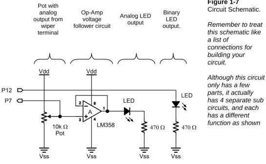
Build the circuit according to the schematic in Figure 1-7. This schematic is like a list of connections between circuit symbols. Try to use this list to build the circuit. Here is a partial list of the connections shown in the schematic:
√ The wiper terminal of the 10 kΩ pot is connected to pin 3 of the LM358 op-amp. √ Pin 2 of the LM358 is connected to pin 1 of the LM358.
√ Pin P7 of the BASIC Stamp is connected to the wiper terminal of the pot. √ Pin 8 of the LM358 is connected to Vdd on your board.
√ Pin 4 of the LM358 is connected to Vss on your board.
Pot with analog output from wiper terminal Op-Amp voltage follower circuit Analog LED output Binary LED output. Figure 1-7 Circuit Schematic. Remember to treat this schematic like a list of
connections for building your circuit.
Although this circuit only has a few parts, it actually has 4 separate sub circuits, and each has a different function as shown
The potentiometer is what makes the analog output. The op-amp is wired to function as a voltage follower. The voltage follower drives the analog LED output. Then there's a separate circuit that uses a BASIC Stamp I/O pin to drive an LED.
Figure 1-8 shows a breadboard example of the schematic from Figure 1-7. For extra tips on building circuits on the breadboard, consult What’s a Microcontroller?
P15 P14 P13 P12 P11 P10 P9 P8 P7 P6 P5 P3 P4 P2 P1 P0 X2 X3 LM 3 5 8 Figure 1-8 Breadboard Example
Compare this breadboard example to the schematic from Figure 1-7. Is the LM358 connected right? Does Vdd go to pin 8 and does Vss go to pin 4?
It turns out that the answer to both questions is yes. Vss is connected by a wire to the lower right terminal on the pot. Then another wire connects from that pot terminal to pin 4 on the LM358.
Since you can follow a wire all the way from pin 4 on the LM358 to the Vss terminal, that means it is in fact connected directly to Vss.
IMPORTANT: Pay careful attention to placing the LM358 so that the index mark (half-circle notch) is to the top, as shown on this breadboard example. If you place it in reverse, the op-amp will be ruined after the battery or power supply is connected to your board.
Programming the Project
The program State_of_P7.bs2 below shows how PBASIC can be used to instruct the BASIC Stamp to do several tasks. First, the BASIC Stamp monitors the state its I/O pin P7, which is set to function as an input. Remember, P7 is connected to the wiper terminal of the pot.
Depending on the analog voltage level at pin P7, the BASIC Stamp interprets the input as low or high (binary 0 or 1). As soon as the input to P7 receives the high signal, the BASIC Stamp sends a high signal to the LED circuit via pin P12. When the input is low, a low signal is sent to P12. The Debug Terminal is also used to monitor the state of pin P7.
Enter Program State_of_P7.bs2 into the BASIC Stamp Editor, and save it under a convenient name, such as State_of_P7_1_1R0.bs2. This stands for Program Listing 1.1 Revision 0. Make sure the programming cable is properly connected to your board, and to the serial or USB port on your computer. Also make sure that a battery or power supply is properly connected, then run the program by clicking the BASIC Stamp Editor’s Run button “►”, or Ctrl-R.
' Basic Analog and Digital - State_of_P7.bs2
' Check the state of P7 and show it on the Debug Terminal. ' {$STAMP BS2} ' {$PBASIC 2.5} DEBUG CLS INPUT 7 OUTPUT 12 DO OUT12 = IN7
DEBUG HOME, "The state of P7 is ", BIN IN7 LOOP
About the Code
The first lines start with an apostrophe. This means that they’re comments and not PBASIC commands. The first line reminds you of the book and file name, for future reference.
' Basic Analog and Digital - State_of_P7.bs2
The second comment is a description of the program. What does the program do?
' Check the state of P7 and show it on the Debug Terminal.
The next two lines are special comments. We call them compiler directives and they are intended to identify the BASIC Stamp and the PBASIC version we are using. For example if you’re following this manual with a BASIC Stamp 2 SX, you might replace the compiler directive “'{$STAMP BS2}” with “'{$STAMP BS2SX}”. (Hint: use the
toolbar buttons to insert these compiler directives.)
' {$STAMP BS2} ' {$PBASIC 2.5}
It's good to start the Debug Terminal and clear it before using it to display data. This way you will avoid inadvertently displaying outputs from previous programs that were in the BASIC Stamp module's memory. The Debug Terminal starts automatically the first time it encounters the DEBUG command in a PBASIC program. This DEBUG command clears
the Debug Terminal after it is opened:
DEBUG CLS
The BASIC Stamp needs to be told how to treat the I/O pins connected to the circuit. They can either be set to function as inputs or outputs.
This PBASIC command sets BASIC Stamp I/O pin P7 to function as an input pin:
INPUT 7
Likewise, I/O pin P12 functions as output with this command:
OUTPUT 12
The rest of the program should be done over and over again, so this is a good place to put
a DO…LOOP loop. So, at the point we want to start to repeat the code we put:
DO
Later in the program, the command LOOP is entered. Each time the program gets to the LOOP command, it returns to DO and starts executing instructions all over again.
The next task is to make the LED connected to pin P12 light up when the voltage at P7 is high enough to qualify as a binary high signal. In other words, if the input value measured at P7 is a binary-1, then the output at P12 should be set to binary-1. Although there are several ways to accomplish this, the easiest way is to set the binary output value of pin P12 equal to the binary input value of pin P7.
OUT12 = IN7
The DEBUG command can be used to display the signal levels received by an I/O pin
functioning as an input in the Debug Terminal. The DEBUG command below prints three
different items. When printing more than one item with a DEBUG command, always
separate each of the items with commas.
DEBUG HOME, "The state of P7 is ", BIN IN7
The first item listed using the DEBUG command is HOME, and it sends the cursor to the
top-left "home" position in the Debug Terminal. Note how HOME is followed by a comma to
separate it from the next item. The next item is a message in quotes: "The state of
pin P7 is ". Whenever you want to display a text message in the Debug Terminal,
use quotes. The third item is BIN IN7, which tells the Debug Terminal to display the
binary input value measured at pin P7.
We want the BASIC Stamp keep checking the voltage at P7 over and over again. We also want the BASIC Stamp to automatically update the LED and the Debug Terminal with the latest information from P7. This is accomplished by repeatedly sending the program back to the DO command we created earlier.
To send the program back to the DO statement to start the process all over again, use the
command:
LOOP
Troubleshooting
Here are a few tips on things to check if your program doesn't work as expected.
• It often takes a few tries to catch all of the wiring mistakes and programming errors.
• The most common mistake is a program entry error. In some cases the BASIC Stamp Editor will tell you there is a mistake. For example if you misspelled a command, the BASIC Stamp Editor will not understand it, and it will tell you which term it didn't understand by highlighting it and displaying a brief message. • In other cases the program will run even though a line of code was typed
incorrectly. For example you might have typed 13 when you meant to type 12. With a mistake like this, when you try to run the program, the LED connected to pin P12 won't light up when you expect it to because the high signal gets sent to pin P13 instead.
• Another common mistake is to plug a wire into the wrong socket on the breadboard. If an LED is not turning on and off the way it should, and there are no programming errors, check the wiring. Also check to make sure the cathode and anode of the LED are connected to the proper places. When an LED is hooked up backwards it won't emit light.
• If the information in the Debug Terminal appears garbled or nonsensical, try closing the Debug Terminal and running the program again.
The Output
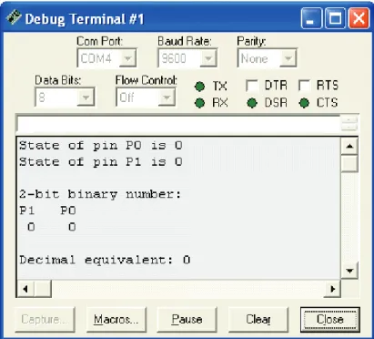
As you adjust the potentiometer knob, note how the LED at the voltage follower's analog output varies in brightness. Meanwhile the LED circuit driven by P12 either turns on or off. This characterizes the difference between analog voltage and digital (binary) voltage. The output displayed in the Debug Terminal should resemble the output shown in Figure 1-9. The state of P7 will either be 0 or 1. Correspondingly, the LED circuit driven by P12 will either be off or on.
Figure 1-9 Debug Terminal Output for Program
Adjust the potentiometer until you have found the threshold voltage. You will know when you've found it because the Debug Terminal will indicate that the state of P7 skips back and forth between 0 and 1 with just the slightest adjustment of the pot. Note the position of the potentiometer. After we build a DC voltmeter in Chapter #3, we can find out how close we are to 1.4 volts, which is the actual threshold voltage of a BASIC Stamp I/O pin when it's functioning as an input.
About the Comparator
Using PBASIC, we programmed the BASIC Stamp to function as a comparator. A comparator is so named because it's a circuit that compares its input voltage to a particular voltage, also called the threshold voltage. If the input voltage is higher than the threshold voltage, the comparator sends a high signal at its output. If the input to the comparator is below the threshold voltage, it sends a low signal.
In the case of our circuit and program, when the analog voltage at pin P7 is below 1.4 volts, the BASIC Stamp sends a low signal (0 volts) at pin P12. When the analog voltage at pin P7 is above 1.4 volts a high signal (5 volts) is sent from pin P12. As you can see in the Debug Terminal, the BASIC Stamp interprets analog input below 1.4 volts as low (binary 0) and input above 1.4 volts as high (binary 1).
Operating a comparator near the threshold voltage is interesting because you can make a small change in voltage at a BASIC Stamp input pin, say from 1.3 to 1.5 volts, and it results in a fairly large change, from 0 to 5 volts at the output.
What have I learned?
On the lines below, insert the appropriate words from the list on the left.
carbon op-amp analog threshold output schematic breadboard
A __________ shows circuit symbols connected to each other by lines. Each circuit symbol corresponds to a component and the lines connecting the symbols work like a list of connections that can be used to guide the construction of a working circuit on a __________.
An __________ is an analog building block that was used in this experiment as a voltage follower.
In this experiment, the potentiometer was used as a source of __________ voltage.
The voltage at the wiper terminal of the potentiometer can be made to vary depending on where the wiper is in contact with the __________ element. A comparator is a device that sends a binary output that depends on whether its analog input is above or below a certain __________ voltage. A comparator can react to a small change in input voltage with a comparatively large change in __________ voltage.
Questions
1. Circle the word that makes the sentence true: The input for a voltage follower is at the ( inverting / non-inverting ) terminal of the op-amp in this experiment. 2. How do you tell the difference between the cathode and the anode on an LED
from your parts kit?
3. If the threshold for a comparator is 2.5 volts, and the input is at 1.5 volts, what's the output going to be?
4. Explain what the command DEBUG HOME does. What has to be done to display
more than one item using a single DEBUG command?
5. What command would you use to set pin P8 to function as an input? Challenge!
1. Add another LED to the circuit to your board and use pin P11 to drive it in an inverted state. In other words, when one LED is on, the other off. Hint: Add 1 to the output value at P11 to invert it.
2. Modify the code from Program State_of_P7.bs2 so that the LED output flashes on and off when the potentiometer output is above the threshold voltage of the BASIC Stamp input pin. Hint: You can use the command pause 500 to make the program pause for half a second.
3. Modify State_of_P7.bs2 to cause one LED to light up when the input voltage at pin P7 is above the threshold voltage and the other LED to light up when the voltage at pin P7 is below threshold voltage.
Why did I learn it?
In this experiment, we compared a binary LED output to an analog LED output. Aside from knowing that the voltage at the wiper terminal had just crossed the threshold voltage, there was no way of indicating the potentiometer's position or the LEDs brightness. On the other hand, in the neighborhood of the threshold voltage, fine variations in analog voltage could be detected.
Even with the limited amount of analog information provided by a binary input, we were able to develop a device called a comparator, which has many applications in electronics design. As we'll discover in a later experiment, the 555 timer chip in you’re A & D parts kit can do some pretty amazing things. This is due in part to two microscopic comparators in the chip.
How can I apply this?
In later experiments, we'll use the threshold voltage to measure the frequency of sound for record and playback purposes. We can also build another type of analog to digital converter using a very simple circuit, the BASIC Stamp and the concept of threshold voltage. We'll use this technique to measure light intensity as well as values for capacitors from the Analog and Digital parts kit.
Chapter #2: Introduction to Bit Crunching
An important step in learning how to make the BASIC Stamp process analog data is learning how to make it send and receive binary numbers. It's also important to understand how binary numbers work, and how to convert from a binary number to a decimal number.
BASIC COMMUNICATION
This experiment introduces some techniques for transmitting and receiving binary numbers using the BASIC Stamp. In this experiment, we'll make a binary keypad for transmitting binary numbers to the BASIC Stamp. The BASIC Stamp will also be programmed to process and display the binary numbers it receives. The binary numbers will be displayed by LEDs as well as by the Debug Terminal. The Debug Terminal will also come in handy for monitoring and displaying the binary numbers in decimal form. In What’s a Microcontroller?, we learned that binary is the number system used by microcontrollers, and that it works with two digits, 0 and 1. The BASIC Stamp is part of an entire class of digital electronic devices that can interpret 0 volts as binary-0 and 5 volts as binary-1.
Binary is useful for describing both states and numbers. In terms of states, the two digits in the binary number system (0 and 1) can be used to describe off/on, closed/open, no/yes, etc. Combinations of binary digits can be used to describe numbers. For example, the binary numbers 101, 110, and 111 describe the decimal numbers 5, 6, and 7. These numbers can in turn be used to describe analog information, such the position of a door as it swings open and closed.
Parts Required (2) 470 Ω resistors (2) 220 Ω resistors (2) 10 kΩ resistors (2) Pushbutton switches (2) Red LEDs
The Pushbutton
There's just one new part and circuit symbol to introduce for this experiment, the pushbutton in Figure 2-1. Note how each terminal on the circuit symbol corresponds to two pins on the part. If you want to connect to a particular terminal shown on the symbol, you can connect to either (or both) of the two corresponding pins on the part.
The open space in the circuit symbol indicates that the switch is normally open. When the two terminals of a switch are not connected, the switch is referred to as an open circuit. Under normal circumstances (when the pushbutton is not pressed), the circuit is open, thus the name normally open.
Figure 2-1 Pushbutton Circuit Symbol Compared to the Component
Building the Circuit
Figure 2-2 shows the schematic for this experiment. Remember to think of a schematic as a list of components and connections. For example, the anode of the right LED is connected to the BASIC Stamp I/O pin P5 socket on your board. The cathode is connected to one terminal of a 470 Ω resistor. The other pin on that same resistor is connected to the Vss terminal on your board, and so on. Follow schematics faithfully when constructing circuits.
Vss Vdd P0 10 kΩ 220 Ω Vss Vdd P1 10 kΩ 220 Ω Vss LED 470 Ω P4 Vss LED 470 Ω P5 Figure 2-2
Schematic featuring two pushbutton circuits and two LED circuits.
Before making a PBASIC program telling the BASIC Stamp how to interface with this circuit, it's essential to understand how the circuit works. The LEDs are pretty straightforward. Set P4 high and the LED lights up; set P4 low and the LED goes dark again. The LED circuit connected to P5 works the same way.
Now, what about the pushbuttons? Let's look at what pin P0 sees when the pushbutton is pressed, then not pressed. When the pushbutton is pressed, P0 gets connected directly to Vdd, which is 5 volts. P0 sees a high signal. When the pushbutton is not pressed, P0 is connected to Vss (0 volts) through the 10 kΩ resistor. Then P0 sees a low signal. This concept applies to both pushbuttons shown in Figure 2-2.
Figure 2-3 shows a breadboard example of the circuit schematic. Of the two BASIC Stamp I/O pins used for the pushbuttons, the lower pin (P0) is connected to the right pushbutton. Likewise, the right pin (P1) is connected to the lower pushbutton. The reason
the wires for the pushbuttons cross relates to the way binary numbers are written, which will be explained later in this experiment.
P 15 P 14 P 13 P 12 P 11 P 10 P 9 P 8 P 7 P 6 P 3 P 2 P4 P5 P 1 P 0 X 2 X3 V dd V ss V in Figure 2-3 Breadboard Example
Entering binary numbers on the pushbuttons will be easiest if you orient your board as shown. Note that the left button is connected to pin P1, and the right button is connected to P0.
Program Listing 2.1 makes the left LED in Figure 2-3 light up when the left pushbutton is pressed. Likewise, the right LED lights up when the right pushbutton is pressed. The program also displays the activity of the pushbuttons in the Debug Terminal.
Programming the Project
Here is a more precise description of the program specifications for the pushbuttons and LEDs.
• When P0 receives a low signal, P5 should send a low signal. • When P0 receives a high signal, P5 should send a high signal. • When P1 receives a low signal, P4 should send a low signal. • When P1 receives a high signal, P4 should send a high signal.
The Debug Terminal can be used to display what the BASIC Stamp receives at pins P0 and P1. DEBUG commands are used to display the binary values the BASIC Stamp
receives as well as their decimal equivalents in the Debug Terminal.
Let's see how this can be done using PBASIC. Enter the Program Listing 2.1 into the BASIC Stamp Editor, and save it as PL2_1R0.bs2. This stands for Program Listing 2.1 Revision 0. Make sure that your board has power and the programming cable is properly connected, then run the program.
' Basic Analog and Digital - PL2_1R0.bs2 ' Program Listing 2.1 Revision 0. ' {$STAMP BS2} ' {$PBASIC 2.5} a VAR Bit b VAR Bit d VAR Nib INPUT 0 INPUT 1 OUTPUT 4 OUTPUT 5 DEBUG CLS DO a = IN0 b = IN1 OUT4 = b OUT5 = a d = (2*b) + (1*a)
DEBUG HOME, "State of pin P0 is ", BIN a, CR DEBUG "State of pin P1 is ", BIN B, CR, CR DEBUG "2-bit binary number: ", CR
DEBUG "P1 P0", CR
DEBUG " ", BIN b, " ", BIN a, CR, CR DEBUG "Decimal equivalent: ", DEC1 d, CR LOOP
The Output
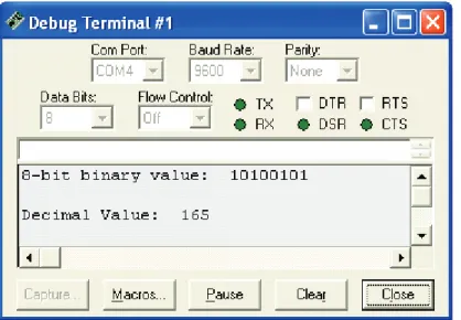
Here's how the program should work. When no pushbuttons are pressed, the Debug Terminal output should match Figure 2-4, and both LEDs should be off. Try pressing the right button (in Figure 2-3). Did the right LED light up? Did the state of P0 in the Debug Terminal change to 1? Is the decimal equivalent 1? If so, it looks like your circuit and program are working well so far.
Figure 2-4 Debug Terminal Output for Program Listing 2.1
So how do you count from decimal-0 to decimal-3 using the binary pushbuttons? The two-bit binary equivalent of decimal-0 is 00. When you don’t press either of the pushbuttons, the decimal output is 0 in the Debug Terminal. When you press the right button, you get 01, which has a decimal equivalent of 1. When you press the left button, you get 10, which has a decimal equivalent of 2. When you press both pushbuttons, you get 11, which has a decimal equivalent of 3.
About the Code
As with the program of the previous chapter, the first lines start with an apostrophe, so they are comments and compiler directives, and the BASIC Stamp ignores them.
' Basic Analog and Digital - PL2_1R0.bs2 ' Program Listing 2.1 Revision 0. ' {$STAMP BS2}
Next, three variables are defined. Variables can be used to store values while the program is running. The letters a and b are defined as variables that store 1-bit each. So,
the variable a can store a single binary digit, likewise with the variable b. The letter d is
defined to be a variable that stores a "nibble" of binary information.
a VAR Bit
b VAR Bit
d VAR Nib
Memory and Food: A bit of memory can store one binary digit, either a 0 or a 1. A nibble of memory stores 4 bits.
A byte (pronounced bite) stores 8 bits. A word stores 16 bits.
Since a bit, a nibble, and a byte, all sound like references to eating food, perhaps a better name for 16 bits might have been "dinner".
This segment of code uses commands introduced in the last chapter. First, two I/O pins are declared inputs and two more pins are declared outputs. Then the Debug Terminal is opened and cleared.
INPUT 0 INPUT 1 OUTPUT 4 OUTPUT 5 DEBUG CLS
We want the BASIC Stamp keep checking the inputs over and over again. We also want the BASIC Stamp to automatically update the LEDs and the Debug Terminal with the latest information on the pushbuttons. The way to accomplish this is to keep repeating the program inside a DO…LOOP loop. To define the start point of the loop we use DO and to
send the program back to this point we’ll use the LOOP command. DO
Next, we need to check the state of the pushbuttons by checking the input at pins P0 and P1. The first of these two commands sets the bit variable a equal to the state measured at
pin P0. The second command sets the bit variable b equal to the state measured at pin P1. a = IN0
Next, we need to set the output at pin P4 equal to the input taken at pin P1. The left LED which is connected to P4 will light up when the left button, which is connected to P1, is pressed. Likewise, we need to set the output at pin P5 equal to the input measured at pin P0.
Since the input values were set to the variables, a and b, we can use a and b to dictate the
output values at pins P4 and P5.
OUT4 = b OUT5 = a
We could just as easily have used the commands OUT4=IN1 and OUT5=IN0; however,
using variables to store the values in memory has advantages as the programs get more complicated. In the next experiment, it will be necessary to use variables to store values. The reason we used variables in this program is because they can be manipulated arithmetically, and the next task is to convert from binary to decimal. To do this, multiply the variable b by 2 and the variable a by 1 and add them together. The nibble variable d is
used to store this new value. This is the method for converting a 2-bit binary number to a decimal number. The next section shows how to do this for a binary number of any size.
d = (2*b) + (1*a)
BASIC Stamp Memory:
RAM: The BASIC Stamp has 26 bytes of RAM (random access memory) that can be used for storing variable values. Another 6 bytes of RAM is used to interface the BASIC Stamp with its I/O pins.
EEPROM: Short for Electrically Erasable Programmable Read Only Memory, EEPROM is used mainly to store the PBASIC programs. EEPROM can also be used to store data values that do not change frequently.
In the calculation we just did using PBASIC, the parentheses are necessary to maintain the normal algebraic order of operation. This is because the BASIC Stamp performs its math beginning at the left. Then, it performs each operation it encounters while checking the line from left to right.
Without the parentheses, d would be set equal to the value ((2 x b + 1) x a) because that's
the order in which the operators (+, -,*, /, etc) are encountered. When parentheses are used, the BASIC Stamp completes operations within parentheses first, and then it does its sweep of operations from left to right.
Six DEBUG commands are used to display all the measured states and the calculated
binary values in the Debug Terminal. The first DEBUG command below displays four
different items. Remember, each item in a single DEBUG command must be separated by a
comma.
The DEBUGHOME command sends the cursor to the top-left "home" position in the Debug
Terminal. Note that it is followed by a comma to separate it from the next item. The next item is a message in quotes: "State of pin P1 is ".
Whenever you want to print a text message to the Debug Terminal, use quotes. The third item is BIN a, which tells the Debug Terminal to print the binary value of the variable a.
The fourth item is CR, which makes the Debug Terminal print a carriage return. DEBUG HOME, "State of pin P0 is ", BIN a, CR
A similar message is printed for the variable b, without the HOME command. The HOME
command works well when it's used once per loop. Remember that DEBUGHOME sends the
cursor to the top-left corner of the Debug Terminal. If we used HOME more than once in
the loop, the information displayed after the first HOME command would be overwritten by
the information following the second HOME command.
DEBUG "State of pin P1 is ", BIN B, CR, CR
Next, two DEBUG commands are used. Each prints a message in quotes followed by two
carriage returns.
DEBUG "2-bit binary number: ", CR
Next, another message in quotes is printed followed by a single carriage return.
DEBUG "P1 P0", CR
In this next command, the quotes contain spaces. The first pair of quotes just contains one space (the space bar on the keyboard was pressed once). Then the binary value of b is
printed, followed by another two spaces in quotes, followed by the binary value of a, then
two more carriage returns.
Here's something new. The modifier DEC was used to print the decimal value of the
variable d. Because this is the last instruction we want to repeat, it’s followed by the LOOP command.
DEBUG "Decimal equivalent: ", DEC1 d, CR LOOP
Counting in Binary
Table 2-1 shows how to count from 0 to 3 using 2-bit binary numbers and how to count from 0 to 7 using 3-bit binary numbers.
Note that four numbers (decimal 0 through 3) can be represented with a 2-bit binary number. Eight numbers (0 through 7) can be represented with a 3-bit binary number. 4 bits can describe 16 different numbers, 5 bits can describe 32 different numbers and so on.
Table 2-1:Measured voltages during charge cycle Decimal number 2-bit binary representation 3-bit binary representation
0 00 000 1 01 001 2 10 010 3 11 011 4 100 5 101 6 110 7 111
You can always determine how many counting numbers (combinations of 0s and 1s) can come from a given number of bits by using this formula:
combinations = 2bits
This means the number of combinations equals two raised to the power of the number of bits. For 2 bits, the number of combinations is 22 = 4. For 3 bits, the number of combinations is 23 = 8, and so on.
Converting from binary to decimal takes two steps. The first step is to multiply each bit by its power of two. Table 2-2 shows the powers of two for up to 8 bits. When you multiply each bit by its value from Table 2-2, you end up with a series of decimal values. The second step is to add up all the decimal values.
Table 2-2: Bit Multipliers for an 8-bit Binary Number
Bit 7 6 5 4 3 2 1 0
Multiplier 128 64 32 16 8 4 2 1
Bit multipliers and Powers of Two: Bit-0 is the least significant bit (LSB) and bit-7 is the most significant bit (MSB). That’s because bit-0 makes the smallest contribution to the number and bit-7 makes the largest contribution. Thinking about a binary number as starting on the left with bit-7 and ending on the right with bit-0 is useful because these numbers indicate the power of 2 for each digit.
Examples:
The multiplier for bit-0 is 1, which equals 20.
The multiplier for bit-1 is 2, which equals 21.
The multiplier for bit-7 is 128, which equals 27.
Note: You can use powers of two to extend Table 2-2 to any number of bits!
As an example, let’s convert binary-1011 to decimal. First, multiply each bit by its power of two from Table 2-2.
8 × 1 = 8
4 × 0 = 0
2 × 1 = 2
1 × 1 = 1
Second, add all 4 of the decimal values:
8 + 0 + 2 + 1 = 11
Parallel and Serial Transmission
Program Listing 2.1 repeats the entire check and report on the pushbutton states routine over and over again. Because the BASIC Stamp checks for input over and over again without waiting for some kind of signal that the data is ready, we are sending the binary numbers to the BASIC Stamp asynchronously.
Asynchronous means not synchronized. In the case of our binary keypad, it means that we change the binary values whenever we want to without waiting for permission from the BASIC Stamp to do so. Likewise, the BASIC Stamp checks the signals at P0 and P1 as fast as it can without waiting for a signal from us that says the data is ready to be checked. We are also sending the binary bits across two separate data lines at the same time. This means we are sending our data bits to the BASIC Stamp in parallel.
The BASIC Stamp has a 16 I/O pins. We could actually send a word-size binary number to the BASIC Stamp in parallel. The problem is that we wouldn't have any pins left for outgoing signals or other input data. When dealing with larger binary numbers, sending serial data instead of parallel data can be useful because it reduces the number of BASIC Stamp I/O pins used to receive data.
When sending serial data, there has to be some way of letting the BASIC Stamp know when each new bit is ready. The BASIC Stamp has built-in functions for sending asynchronous as well as synchronous serial data.
In this next example, the same two pushbuttons are used to send the BASIC Stamp a nibble (4 bits) of serial, synchronous data. The result is displayed in the Debug Terminal.
Parallel means the data bits are sent across more than one data line at the same time. We just finished using the pushbuttons to send two parallel bits.
Serial: Instead of sending data in parallel along multiple data lines, a single data line can be used and the data bits can be sent one after another.
Synchronous: Sending data synchronously means we are sending the data in a time- coordinated manner (in sync). Technically, it means that the sender and receiver of the data bits do so according to signals from the same clock
Reprogramming to Receive Serial Data
Enter Program Listing 2.2 into the BASIC Stamp Editor, and save it under the name PL2_2R0.bs2.
' Basic Analog and Digital - PL2_2R0.bs2 ' Program Listing 2.2 Revision 0. ' {$STAMP BS2} ' {$PBASIC 2.5} n VAR Nib d VAR Nib INPUT 0 INPUT 1 FOR n = 1 TO 4 DO
'Wait for high LOOP UNTIL IN1=1
DO
'Wait for low LOOP UNTIL IN1=0
d = d << 1 d = d + IN0
DEBUG HOME, "Shifting in bits: ", BIN4 d NEXT
DEBUG CR, CR, "Done shifting.", CR, CR DEBUG "Decimal value: ", DEC2 d, CR, CR
The Output
The Debug Terminal will initially show a blank screen when you run the program. Follow these instructions carefully to send the synchronous, serial data. First, press and hold the right button. Then press and release the left button. The output should look like Figure 2-5 below.
Figure 2-5 Debug Terminal Output for Program Listing 2.2.
Next, release the right button, and press and release the left button again. The output should change so that it looks like Figure 2-6.
Figure 2-6 Debug Terminal Output for Program Listing 2.2.
Press and hold the right button, then press and release the left button twice. Then the output should look like Figure 2-7.
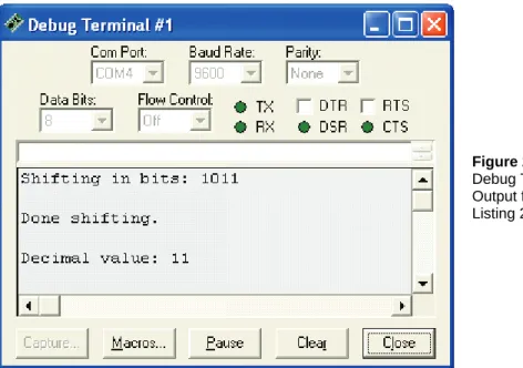
Figure 2-7 Debug Terminal Output for Program Listing 2.2.
If your program worked as shown, you just synchronously shifted 4 serial bits into the BASIC Stamp's RAM. In addition, it was verified that the decimal value of binary-1011 really is 11 in the decimal number system.
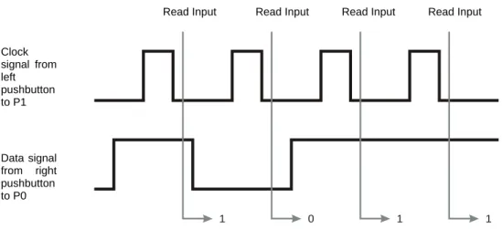
Figure 2-8 shows how these events occurred (from left to right) in a timing diagram. The left pushbutton was the clock signal. The clock signal consisted of a series of clock pulses. Each clock pulse was the press and release of the left pushbutton. This sent a low-high-low signal to P1. Each time the left pushbutton was released, the BASIC Stamp checked the state of the data line, which was the state of the right pushbutton (P0). The BASIC Stamp is programmed to read the input data after the clock signal's transition from high to low. This transition is referred to as the negative edge of the clock pulse.
Read Input Read Input Read Input Read Input Clock signal from left pushbutton to P1 Data signal from right pushbutton to P0 1 0 1 1
Figure 2-8: Timing Diagram.
About the Code
Like Program Listing 2.1, we use a comment to include some information about the program at the beginning. Remember, as soon as an apostrophe appears in a line of PBASIC code, everything to the right of the apostrophe is ignored by the BASIC Stamp. Next the two nibble variables are defined, and I/O pins P0 and P1 are set to function as inputs. One of those nibble variables, n, is used by the FOR…NEXT loop.
The main portion of the code is in a FOR…NEXT loop, which has the following syntax:
FOR Counter = StartValue TO EndValue
In the example code snippet below, n is the Counter, 1 is the StartValue argument and 4 is
the EndValue argument of the FOR…NEXT command.
FOR n = 1 TO 4 DEBUG DEC n, CR NEXT
This FOR…NEXT loop executes the PBASIC command between the FOR command and the NEXT command four times. The first time through the loop the value of n is 1, the second
time through the value of n increments to 2, and so on until n gets to 4. After completing
the 4th pass, the program skips out of the loop and continues on to the line of code after the NEXT command.
Program Listing 2.2 has a more complicated set of commands that gets repeated within
its FOR…NEXT loop, and it is different from what we've seen before. It starts with a
DO…LOOP conditional loop. This loop is used to check the value at pin P0. If the value of
P0 is low, LOOP UNTIL IN1=1 sends the program back to DO. If the value at pin P1 is
high, then the program executes the next line, after the LOOP instruction. FOR n = 1 TO 4
DO
'Wait for high LOOP UNTIL IN1=1
The same technique is applied with the next two lines of code (and one comment), which repeat themselves until a low signal is received.
DO
'Wait for low LOOP UNTIL IN1=0
The command d=d<<1 shifts all the bits in d left by 1. When values are shifted, the
vacant space in the rightmost bit (the LSB) is automatically filled with a zero. Then the bit value at pin P0 is loaded into the LSB position in the nibble. This is done using the
d=d+IN0 command, which adds the single bit measured at P0 to the value of the nibble
variable d. The second time through the loop, the value that was placed in the LSB gets shifted left by one, so it ends up in bit-1. Meanwhile the next value sampled at P0 is placed in the LSB slot. The shift and add process is repeated four times as each bit is shifted into the byte.
d = d << 1 d = d + IN0
Each time a new bit is shifted in, we use the DEBUG command to display the new value.
Each time the program gets to the NEXT command it returns to the FOR n = 1 TO 4
command, and the value of n is incremented, until it gets to 4. Finally the program breaks
DEBUG HOME, "Shifting in bits: ", BIN4 d NEXT
Once the FOR…NEXT loop is finished and all the bits are shifted into the d variable, two
messages are printed. The second of the two DEBUG commands has a new modifier, DEC2.
This modifier is used to make the Debug Terminal display the value of d as two decimal
digits.
DEBUG CR, CR, "Done shifting.", CR, CR DEBUG "Decimal value: ", DEC2 d, CR, CR
While Chapter 1 introduced analog voltage, this chapter introduced the basics of sending and receiving binary numbers. In the next experiment, we'll combine these topics to build a digital DC voltmeter, which is a device that measures analog voltage and displays the measurement as a digital value.
What have I learned?
On the lines below, insert the appropriate words from the list on the left.
largest word decimal BASIC Stamp synchronously LSB PBASIC byte binary numbers
The _____________ can be used to process information about analog measurements using _____________ . Before working with analog to digital interfaces, it's important to understand how the BASIC Stamp sends, receives, and stores binary data. It's also important to be able to use _____________ to program the BASIC Stamp to send, receive, and store binary data.
When converting a binary number to its _____________ equivalent, each bit should be multiplied by a particular power of two. The _____________ is the rightmost bit in a binary number, and it makes the smallest contribution to the value of that number. It is also referenced as bit-0. The MSB is the leftmost bit. It makes the _____________ contribution to the value of a binary number. The bit just to the left of the LSB is bit-1, the bit 2 bits to the left of LSB is bit-2 and so on. The BASIC Stamp can store a single bit, a nibble, which is 4 bits, a _____________, which is 8 bits, or a _____________, which is 16 bits. To save I/O pins, the BASIC Stamp can send and receive serial data as opposed to parallel data, which uses multiple data lines. Binary data can also be sent _____________ or asynchronously.
Questions
1. Determine the decimal equivalents of these binary numbers: 1010, 1111, 0010, and 0100.
2. The command d = d<<1 was used to shift the bits in the variable d to the left by
1. What command do you think would be used to shift the bits to the right? What command would you use to shift the bits by, say, 3 to the left?
3. Explain the difference between serial and parallel data.
4. Explain the difference between synchronous and asynchronous data transmission.
Challenge!
1. Program Listing 2.1 is used to count to three. Write a program that uses three parallel bits (use pin P2 for the third bit) and counts to 7. You can check your work by connecting the input pin P2 to Vdd for a high signal and to Vss for a low signal (using a 1 kΩ resistor).
2. Modify Program Listing 2.2 so that it displays the clock pulses you apply to the left pushbutton with the left LED.
3. Modify Program Listing 2.2 so that it shifts the bits back out, displaying them with the right LED.
Why did I learn it?
The goal in this series of experiments is to demonstrate how a device such as the BASIC Stamp, which processes binary data, can be used to interface with the analog world. Binary numbers and states form the foundation for how microcontrollers, microprocessors and an entire class of binary circuits process data.
Analog data can be effectively processed with binary numbers using the techniques in this experiment. Learning the basics of processing binary data will help make a myriad of electronic circuits easier to understand. This is also the foundation for how the home computer processes data. Understanding data at the binary level ("bit crunching") also makes various programming languages easier to understand.
How can I apply this?
In some of the upcoming experiments, we will process analog data using serial and parallel data. We will also use synchronous and asynchronous communication. The BASIC Stamp can be connected to other integrated circuits and exchange binary data. The BASIC Stamp can also be programmed to convert the binary data to a meaningful decimal form.
We'll use these techniques to measure voltage, sound, light, etc.
The BASIC Stamp has commands which automate the serial data transmit and receive processes in both asynchronous and synchronous modes. We will encounter the serial, synchronous method in Chapter #3. The BASIC Stamp also has features available to simplify the sending and receiving of parallel data, as we'll discover in Chapter #4 where asynchronous parallel data is transmitted.
Chapter #3: Basic Analog to Digital Conversion
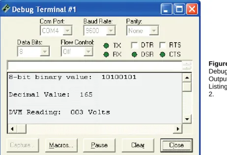
BUILD YOUR OWN DIGITAL DC VOLTMETERA digital DC voltmeter (DC DVM) is a handy tool for measuring voltage between two contact points. In this experiment, we will build a DVM for measuring DC voltage in the 0 to 5 volt range. A common use for a DC DVM is testing the voltage (potential) between the two terminals on a battery.
A digital voltmeter is so named because it displays its measurements with digits. The digits 0 through 9 and a decimal point are used to display the voltage measurements as decimal values. The digits 0 and 1 could be used. It would still be a "digital" voltmeter, but it would have binary display instead of a decimal display. Making sense out of each measurement would be time consuming. Since our DVM processes its measurements in binary, we'll start with a binary display and then modify it to a more conventional and easy to read decimal display.
In Chapter #1, we used an LED circuit to display changes in analog voltage level applied to a circuit. As a “continuously variable value”, analog voltage varies within a continuous range. We'll use the potentiometer as we did in Chapter #1 to make a range of voltages that can vary continuously between 0 and 5 volts.
Although information about analog voltage can be processed efficiently with binary devices, the voltage has to be sampled and described using binary numbers first. The ADC0831 is a common integrated circuit that does this job. It describes the analog information with binary numbers for devices that process binary information, such as the BASIC Stamp.
In this experiment, we will make a DVM using the BASIC Stamp together with the ADC0831 integrated circuit. A pot will be wired to your Board of Education or HomeWork Board and adjusted to make analog output voltage. The DVM will then be used to measure samples from the pot’s continuous range of voltage outputs.
Continuous range: A minimum value, a maximum value, and everything in between. When a source of voltage varies over a continuous range, it is considered an analog voltage. We will use our DVM to sample voltages over a continuous range, from 0 to 5 volts. So, the voltage we measure might be 1.234 volts or 3.857564… volts, or 4.9999… volts, etc.