Worcester Polytechnic Institute
Digital WPI
Masters Theses (All Theses, All Years) Electronic Theses and Dissertations
2015-04-29
Video/Image Processing on FPGA
Jin Zhao
Worcester Polytechnic Institute
Follow this and additional works at:https://digitalcommons.wpi.edu/etd-theses
This thesis is brought to you for free and open access byDigital WPI. It has been accepted for inclusion in Masters Theses (All Theses, All Years) by an authorized administrator of Digital WPI. For more information, please [email protected].
Repository Citation
Zhao, Jin, "Video/Image Processing on FPGA" (2015).Masters Theses (All Theses, All Years). 503. https://digitalcommons.wpi.edu/etd-theses/503
Video/Image Processing on FPGA
by Jin Zhao A Thesis
Submitted to the Faculty of the
WORCESTER POLYTECHNIC INSTITUTE In partial fulfillment of the requirements for the
Degree of Master of Science in
Electrical and Computer Engineering by
April 2015 APPROVED:
Professor Xinming Huang, Major Thesis Advisor
Professor Lifeng Lai
Abstract
Video/Image processing is a fundamental issue in computer science. It is widely used for a broad range of applications, such as weather prediction, computerized tomography (CT), artificial intelligence (AI), and etc. Video-based advanced driver assistance system (ADAS) attracts great attention in recent years, which aims at helping drivers to become more concentrated when driving and giving proper warn-ings if any danger is insight. Typical ADAS includes lane departure warning, traffic sign detection, pedestrian detection, and etc. Both basic and advanced video/image processing technologies are deployed in video-based driver assistance system. The key requirements of driver assistance system are rapid processing time and low power consumption. We consider Field Programmable Gate Array (FPGA) as the most appropriate embedded platform for ADAS. Owing to the parallel architecture, an FPGA is able to perform high-speed video processing such that it could issue warn-ings timely and provide drivers longer time to response. Besides, the cost and power consumption of modern FPGAs, particular small size FPGAs, are considerably ef-ficient. Compared to the CPU implementation, the FPGA video/image processing achieves about tens of times speedup for video-based driver assistance system and other applications.
Acknowledgements
I would like to sincerely express my gratitude to my advisor, Professor Xinming Huang. He offered me the opportunity to study and develop myself in Worcester Polytechnic Institute, guided me in the research projects and mentored me in my life.
Thanks to Sichao Zhu for his creative and helpful work in the traffic sign detection project. Thanks to Bingqian Xie for her ideas and experiments in the lane departure warning system project. Thanks to Boyang Li for helping me learn how to build basic video/image processing block using Mathworks tools.
Thanks to The Mathworks. Inc for their generously supporting our research, financially and professionally.
Thanks to all my lovely friends and my family for their help in the past years. They always encourage me and give me confidence to overcome all the problems.
Contents
1 Introduction 1
2 Basic Video/Image Processing 3
2.1 Digital Image/Video Fundamentals . . . 3
2.2 Mathworks HDL Coder Introduction . . . 5
2.3 Color Correction . . . 7 2.3.1 Introduction . . . 7 2.3.2 Simulink Implementation . . . 8 2.3.3 FPGA Implementation . . . 11 2.4 RGB2YUV . . . 15 2.4.1 Introduction . . . 15 2.4.2 Simulink Implementation . . . 17 2.4.3 FPGA Implementation . . . 18 2.5 Gamma Correction . . . 19 2.5.1 Introduction . . . 19 2.5.2 Simulink Implementation . . . 21 2.5.3 FPGA Implementation . . . 22 2.6 2D FIR Filter . . . 23 2.6.1 Introduction . . . 23
2.6.2 Simulink Implementation . . . 26 2.6.3 FPGA Implementation . . . 28 2.7 Median Filter . . . 29 2.7.1 Introduction . . . 29 2.7.2 Simulink Implementation . . . 30 2.7.3 FPGA Implementation . . . 33 2.8 Sobel Filter . . . 34 2.8.1 Introduction . . . 34 2.8.2 Simulink Implementation . . . 35 2.8.3 FPGA Implementation . . . 36
2.9 Grayscale to Binary Image . . . 37
2.9.1 Introduction . . . 37
2.9.2 Simulink Implementation . . . 39
2.9.3 FPGA Implementation . . . 41
2.10 Binary/Morphological Image Processing . . . 41
2.10.1 Introduction . . . 41
2.10.2 Simulink Implementation . . . 43
2.10.3 FPGA Implementation . . . 44
2.11 Summary . . . 45
3 Advanced Video/Image Processing 46 3.1 Lane Departure warning system . . . 46
3.1.1 Introduction . . . 46
3.1.2 Approaches to Lane Departure Warning . . . 47
3.1.3 Hardware Implementation . . . 52
3.1.4 Experimental Results . . . 56
3.2.1 Introduction . . . 58
3.2.2 SURF Algorithm . . . 59
3.2.3 FPGA Implementation of SURF . . . 61
3.2.3.1 Overall system architecture . . . 62
3.2.3.2 Integral image generation . . . 63
3.2.3.3 Interest points detector . . . 64
3.2.3.4 Memory management unit . . . 67
3.2.3.5 Interest point descriptor . . . 68
3.2.3.6 Descriptor Comparator . . . 69
3.2.4 Results . . . 70
3.3 Traffic Sign Detection System Using SURF and FREAK . . . 71
3.3.1 FREAK Descriptor . . . 72
3.3.2 Hardware Implementation . . . 73
3.3.2.1 Overall System Architecture . . . 73
3.3.2.2 Integral Image Generator and Interest Point Detector 74 3.3.2.3 Memory Management Unit . . . 75
3.3.2.4 FREAK Descriptor . . . 76
3.3.2.5 Descriptor Matching Module . . . 77
3.3.3 Results . . . 78
3.4 Summary . . . 79
List of Figures
1.1 Xilinx KC705 development kit . . . 2
2.1 Video stream timing signals . . . 5
2.2 HDL supported Simulink library . . . 6
2.3 Illustration of color correction . . . 8
2.4 Flow chart of color correction system in Simulink . . . 9
2.5 Flow chart of video format conversion block . . . 10
2.6 Flow chart of serialize block . . . 10
2.7 Flow chart of deserialize block . . . 10
2.8 Implementation of color correction block in Simulink . . . 11
2.9 Example of color correction in Simulink . . . 12
2.10 HDL coder workflow advisor (1) . . . 13
2.11 HDL coder workflow advisor (2) . . . 13
2.12 HDL coder workflow advisor (3) . . . 14
2.13 HDL coder workflow advisor (4) . . . 14
2.14 HDL coder workflow advisor (5) . . . 15
2.15 Example of color correction on hardware . . . 15
2.16 Illustration of RGB to YUV conversion . . . 16
2.17 Flow chart of RGB2YUV Simulink system . . . 17
2.19 Example of RGB2YUV in Simulink . . . 19
2.20 Example of RGB2YUV on hardware . . . 20
2.21 Illustration of gamma correction . . . 21
2.22 Flow chart of gamma correction system in Simulink . . . 22
2.23 Parameter settings for 1-D Lookup Table . . . 22
2.24 Example of gamma correction in Simulink . . . 23
2.25 Example of gamma correction on hardware . . . 24
2.26 Illustration of 2D FIR filter . . . 25
2.27 Flow chart of 2D FIR filter system in Simulink . . . 26
2.28 Flow chart of 2D FIR filter block in Simulink . . . 26
2.29 Flow chart of Sobel Kernel block . . . 27
2.30 Architecture of kernel mult block . . . 27
2.31 Example of 2D FIR filter in Simulink . . . 28
2.32 Example of 2D FIR filter on hardware . . . 28
2.33 Illustration of median filter . . . 30
2.34 Flow chart of median filter block in Simulink . . . 31
2.35 Flow chart of the median Simulink block . . . 31
2.36 Architecture of the compare block in Simulink . . . 32
2.37 Implementation of basic compare block in Simulink . . . 32
2.38 Example of median filter in Simulink . . . 33
2.39 Example of median filter on hardware . . . 34
2.40 Illustration of Sobel filter . . . 35
2.41 Flow chart of Sobel filter block in Simulink . . . 35
2.42 Flow chart of the Sobel kernel block in Simulink . . . 36
2.43 Flow chart of the x/y directional block in Sobel filter system . . . 37
2.45 Example of Sobel filter on hardware . . . 38
2.46 Illustration of grayscale to binary image conversion . . . 39
2.47 Flow chart of the proposed grayscale to binary image conversion systems 40 2.48 Implementation of the gray2bin block in Simulink . . . 40
2.49 Example of grayscale to binary image conversion in Simulink . . . 40
2.50 Example of grayscale to binary image conversion on hardware . . . . 41
2.51 Illustration of morphological image processing . . . 43
2.52 Flow chart of the proposed image dilation block . . . 44
2.53 Detail of the bit operation block . . . 44
2.54 Example of image dilation in Simulink . . . 45
2.55 Example of image dilation on hardware . . . 45
3.1 Flow chart of the proposed LDW and FCW systems . . . 48
3.2 Illustration of Sobel filter and Otsu’s threshold binarization. (a) is the original image captured from camera. (b) and (c) are ROI after Sobel filtering and binarization, respectively . . . 50
3.3 Hough transform from 2D space to Hough space . . . 51
3.4 Sobel filter architecture . . . 53
3.5 Datapath for Otsu’s threshold calculation . . . 53
3.6 Hough transform architecture . . . 54
3.7 Flow chart of front vehicle detection . . . 55
3.8 Results of our LDW and FCW systems . . . 57
3.9 Overall system block diagram . . . 62
3.10 Integral image generation block diagram . . . 63
3.11 Build Hessian Response block diagram . . . 65
3.12 Is Extreme block diagram . . . 66
3.14 Traffic sign detection system . . . 71
3.15 Illustration of the FREAK sampling pattern . . . 72
3.16 FPGA design system block diagram . . . 74
3.17 Integral image address generator. . . 75
3.18 Normalized intensity calculation. . . 76
3.19 Descriptor matching flow chart . . . 77
List of Tables
3.1 Device utilization summary . . . 56 3.2 Device utilization summary . . . 71 3.3 Device utilization summary . . . 78
Chapter 1
Introduction
Video/image processing is any form of signal processing for which the input is an video/image, such as a video stream or photograph. Video/image needs to be pro-cessed for better display, storage and other special purposes. For example, medical scientists enhance x-ray images and suppress accompanying noises for doctors to make precise diagnosis. Video/image processing also builds solid groundwork for computer vision, video/image compression, machine learning and etc.
In this thesis we focus on real-time video/image processing for advanced driver assistance system (ADAS). Each year millions of traffic accidents occurred around the world cause loss of lives and property. Improving road safety through advanced computing and sensor technologies has drawn lots of interests from researchers and corporations. Video-based driver-assistance system is becoming an indispensable part of smart vehicles. It monitors and interprets the surrounding traffic situation, which greatly improves driving safety. ADAS includes, but is not limited to, lane departure warning, traffic sign detection, pedestrian detection, etc. Unlike general video/image processing on computer, driver assistance system naturally requires rapid video/image processing as well as low power consumption. Alternative solution
should be considered for ADAS rather than general purpose CPU.
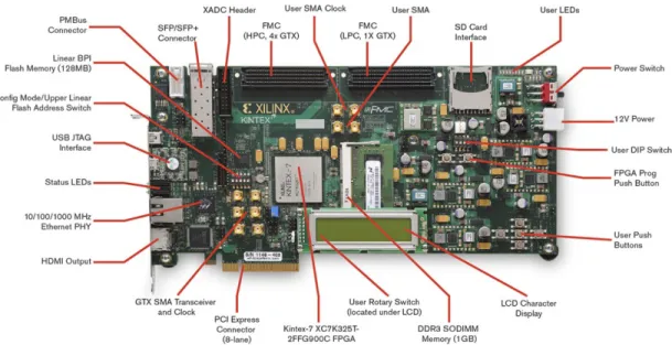
Field Programmable Gate Array (FPGA) is an reconfigurable integrated circuit. Its parallel computational architecture an convenient access to local memories make it the most appropriate platform for driver assistance system. An FPGA is able to perform real-time video processing such that it could issue corresponding warnings to the drivers timely. Besides, the cost and power consumption of modern FPGAs are relatively low, compared to CPU and GPU. In this thesis work, we employ Xilinx KC705 FPGA development kit in figure 1.1 as the hardware platform.
Figure 1.1: Xilinx KC705 development kit
This thesis is organized as follows. Chapter 2 introduces the basic video/image processing blocks and their implementation on FPGA. Chapter 3 presents advanced video/image processing algorithms for driver assistance system and their FPGA implementation. Chapter 4 concludes our achievements and possible improvement in the work of future.
Chapter 2
Basic Video/Image Processing
This chapter starts with introduction of digital video/image, then presents basic video/image processing blocks. Basic video/image processing is not only broadly used in simple video systems, but could be fundamental and indispensable compo-nent in complex video projects. In the thesis, we cover the following video pro-cessing functions: color correction, RGB to YUV conversion, gamma correction, median filter, 2D FIR filter, Sobel filter, grayscale to binary conversion and mor-phological image processing. For every functional block, this thesis introduces basic idea, builds the blocks using Mathworks Simulink and HDL Coder toolbox, and implements hardware block on FPGA.
2.1
Digital Image/Video Fundamentals
A digital image could be defined as a two-dimensional function f(x, y), where the
x and y are spatial coordinates, and the amplitude off(x, y) at any location of an image is called the intensity of the image at that point as (2.1).
f = f(1,1) f(1,2) · · · f(1, n) f(2,1) f(2,2) · · · f(2, n) .. . ... ... f(m,1) f(m,2) · · · f(m, n) (2.1)
Color image includes color information for each pixel. It could be seen as a combination of individual images of different color channels. The mainly used color system in computer displays are RGB (Red, Green, Blue) space. Other color image representation systems are HSI (Hue, Saturation, Intensity) and YCbCr or YUV.
Grayscale image refers to monochrome image. The only color of each pixel is shade of gray. In fact, a gray color is one in which the red, green and blue components all have equal intensity in RGB space. Hence, it is only necessary to specify a single intensity value for each pixel, as opposed to represent each pixel with three intensities in full color images.
For each color channel of RGB image and grayscale image pixel, the intensity is within a given range between a minimum and maximum value. Often, every pixel intensity is stored using an 8-bit integer giving 256 possible different grades from 0 and 255. The black is 0 and the white is 255, respectively.
Binary image, or black and white image, is a kind of digital image that has only two possible intensity value for every pixel, 1 as white and 0 for black. The object is labeled with foreground color while the rest of the image is with the background color.
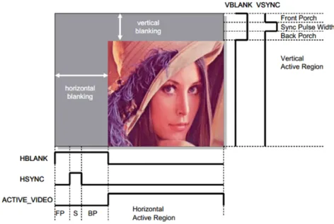
Video stream is a series of successive images. Every video frame consists of active pixels and blanking as figure 2.1. At the end of each line, there is a portion of waveform called horizontal blanking interval. The horizontal sync signal ’hsync’ indicates start of the next line. Starting from the top, all the active lines on the
Figure 2.1: Video stream timing signals
display area are scanned in this way. Once the entire active video frame is scanned, there is another portion of waveform called vertical blanking interval. The vertical sync signal ’vsync’ indicates start of the new video frame. The time slot of blanking could be used to process video stream, which we can see in the following chapters.
2.2
Mathworks HDL Coder Introduction
Matlab/Simulink is a high-level language for scientific and technical computing in-troduced by Mathworks, Inc. Matlab/Simulink takes matrix as basic data element and makes tremendous matrix operation optimization. Therefore, Matlab is perfect for video/image processing since video/image is naturally matrix.
HDL coder is a Matlab toolbox product. It generates portable, synthesizable Verilog and VHDL code from Mathworks Matlab, Simulink and Stateflow charts. The generated HDL code can be used for FPGA programming or ASIC (Application Specific Integrated Circuit) prototyping and design. HDL Coder provides a workflow advisor that automates the programming of Xilinx and Altera FPGAs. You can
control HDL architecture and implementation, highlight critical paths, and generate hardware resource utilization estimates.
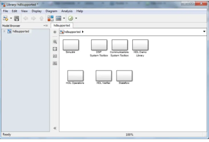
Compared to HDL code generation from Matlab, Simulink provides graphical programming tool for modeling, which is more suitable for building image/video processing blocks. Furthermore, HDL Coder provides traceability between your Simulink model and the generated Verilog and VHDL code. To look up what blocks in Simulink support HDL generation, just type ’hdllib’ in Matlab command line. A window will be prompted as in figure 2.2 and customs could find all the HDL friendly Simulink blocks. In order to successfully generate HDL code, every model in the subsystem must be from the hdlsupported library.
Figure 2.2: HDL supported Simulink library
In the following content of this chapter, we will focus on construct basic im-age/video processing system in Simulink environment using HDL friendly models. The Simulink settings and workflow to generate HDL code are also advised.
2.3
Color Correction
2.3.1
Introduction
Color inaccuracies exist commonly during image/video acquisition. An error white balance setting or inappropriate color temperature will produce color errors. In most digital still and video imaging systems, color correction is to alter the overall color of the light. In RGB color space, color image is stored in m×n×3 arrays and each pixel could be represented as 3D vector [R, G, B]0. The color channel correction matrix M is applied to the input images in order to correct color inaccuracies. The correction could be expressed by an multiplication as the following equality in (2.2):
Rout Gout Bout = M11 M12 M13 M21 M22 M23 M31 M32 M33 × Rin Gin Bin (2.2) or be unfolded in 3 items as Rout =M11×Rin+M12×Gin+M13×Bin (2.3) Gout =M21×Rin+M22×Gin+M23×Bin (2.4) Bout =M31×Rin+M32×Gin+M33×Bin (2.5)
There are several solution to estimate the color correction matrix. For example, Least-squares solution could make the matrix more robust and less influenced by outliers. In the typical workflow, a test chart with known and randomly distributed color patches was captured by a digital camera with “auto” white balance.
Com-parison of means of the red, green and blue color components in the color patches, original versus captured, reveal the presence of non-linearity. The non-linearity could be described using a 3×3 matrix N. In order to accurately display the real color, we employ inverse matrix M = N−1 to offset non-linearity of video camera. For example, In fig. 2.3, (a) is the generated original color patches. (b) is image (a) with color inaccuracies. All the color patches seem containing more red compo-nents. The color drifting could be modeled with matrix N and we could correct the incorrect color patches with M =N−1 and get recovered image (c).
(a) (b) (c)
Figure 2.3: Illustration of color correction
2.3.2
Simulink Implementation
Simulink, provided by Mathworks, is a graphical block diagram environment for modeling, simulating and analyzing multi-domain dynamic systems. Its interface is a block diagramming tool and a set of block libraries. It supports simulation, verification and automatic code generation.
method is pretty straightforward: 1) create a new Simulink model. 2) type ’simulink’ in Matlab command line to view all available Simulink library blocks. 3) type ’hdl-lib’ in Matlab command line and open all Simulink block that support HDL code generation. 4) use these HDL friendly block to build up functional blocks hierar-chically. You can do so by copying blocks from Simulink library and hdlsupported library to your Simulink model, then simply draw connection lines to link blocks.
Simulink simulates a dynamic system by computing the states of all blocks at a series of time steps over a chosen time span, using information defined by the model. The Simulink library of solvers is divided into two major types: fixed-step and variable-step. They can further be divided within each of these categories as: discrete or continuous, explicit or implicit, one-step or multi-step, and single-order or variable-single-order. For all the image processing demos in this thesis, variable step discrete solver is selected. You can go to Simulink → Model Configuration Parameters and select correct solver in the Solver tab of prompted window.
We will elaborate the basic steps and other algorithms in this chapter follow the same guideline. It is important to point out that we just need to translate key processing algorithms to HDL and so other parts of Simulink model, such as source, sink, pre-processing and etc, are not necessarily from hdlsupported library.
Figure 2.4: Flow chart of color correction system in Simulink
Figure 2.4 gives a big picture of the entire color correction Simulink system. The state flow is as follow: The source block takes image as system input. Video Format Conversion block concatenates three color components to a single bus as
in Figure 2.5. Serialize block converts image matrix to pixel-by-pixel stream. Fig. 2.6 illustrates the inner structure of Serialize block. Color correction block is the key componentamong those modules. This block must be purely set up with funda-mental blocks from hdlsupported library and hence could be translated to Verilog and VHDL using HDL coder work flow. The subsequent Serialize block as fig. 2.7, inverse of Serialize, convert serial pixel stream back to image matrix. The final block - Video Viewer displays filtering result in Simulink.
Figure 2.5: Flow chart of video format conversion block
Figure 2.6: Flow chart of serialize block
Figure 2.7: Flow chart of deserialize block
Fig. 2.8 illustrates color correction block Simulink implementation. The input bus signal is separated to three color components RGB. The gain blocks implement multiplication. The sum blocks sum up previous multiplication products. Matrix
multiplication is implemented using these gain and sum blocks. Finally the corrected color components are concatenated again to a bus signal. The delay blocks inserted in between will be transferred to registers in hardware, which add more clock cycles to leverage higher clock frequency.
Figure 2.8: Implementation of color correction block in Simulink
Fig 2.9 gives the simulation result in Simulink environment. Image (a) is the RGB image with color inaccuracy and image (b) is the corrected image using color correction Simulink system.
2.3.3
FPGA Implementation
After successfully making a functional Simulink project based on HDL friendly basic blocks, we could simply generate HDL code from it using Mathworks HDL coder toolbox.
(a) (b)
Figure 2.9: Example of color correction in Simulink
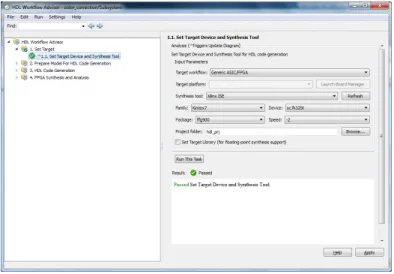
In the first step, right click the HDL friendly subsystem and select HDL Code → HDL Workflow Advisor. In the Set Target → Set Target Device and Synthesis Tool step, for Synthesis tool, select Xilinx ISE and click Run This Task as in fig. 2.10.
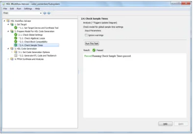
In the second step as in fig. 2.12, right-click Prepare Model For HDL Code Gen-eration and select Run All. The HDL Workflow Advisor checks the model for code generation compatibility. You may encounter some incorrect model configuration settings problems for HDL code generation as figure 2.11. To fix the problem, click the Modify All button, or click the hyperlink to launch the Configuration Parameter dialog and manually apply the recommended settings.
In the HDL Code Generation → Set Code Generation Options → Set Basic Options step, select the following options, then click Apply: For Language, select Verilog, Enable Generate traceability report, Enable Generate resource utilization report. For the options available in the Optimization and Coding style tabs, you can use these options to modify the implementation and format of the generated code. This step is showed in fig. 2.13.
Figure 2.10: HDL coder workflow advisor (1)
Figure 2.11: HDL coder workflow advisor (2)
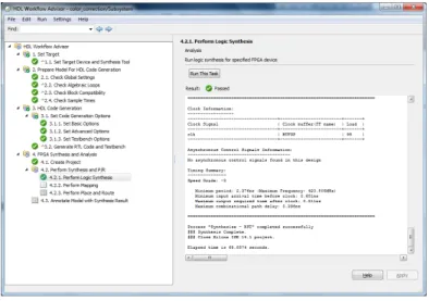
After Simulink successfully generate HDL code, you have two ways to synthesize and analyze the generated HDL code: 1) copy the HDL code to your HDL project and run the synthesis, translation, mapping and P&R in Xilinx ISE environment manually. 2) run those task in Simulink environment as in fig. 2.14.
In order to validate the entire color correction design, we conduct an experiment on a KC705 FPGA platform. The video streams from a camera or computer are sent to an on-board Kintex-7 FPGA via FMC module. The FPGA performs color
Figure 2.12: HDL coder workflow advisor (3)
Figure 2.13: HDL coder workflow advisor (4)
correction on every video frame and exports the results to a monitor for display. We delay the video pixel timing signals vsync, hsync and de accordingly to match pixel delay cycles in Simulink.
The reported maximum frequency is 228.94 MHz. The resources utilization of the color correction system on FPGA is as follows : 102 slice registers and 246 slice LUTs. Fig. 2.15 illustrates the result of our color correction system on hardware. Image (a) is an video image with color inaccuracy and image (b) is the corrected
Figure 2.14: HDL coder workflow advisor (5)
(a) (b)
Figure 2.15: Example of color correction on hardware image with accurate color.
2.4
RGB2YUV
2.4.1
Introduction
Color image processing is a logical extension to the processing of grayscale images. The main difference is that each pixel consists of a vector of components rather
than a scalar. Usually, a pixel from an image has three components: red, green and blue. These are defined by the human visual system. Color is typically represented by a three dimensional vector and user can define how many bits each component have. Besides using RGB to represent the color of an image, there are different ways to represent an image to make subsequent analysis or processing easier, such as CMYK (subtractive color model, mainly used in color printing) and YUV (used for video/image compression and television system). Here Y stands for luminance signal, which is the combination of RGB components, with the color provided by two color difference signals U and V.
Because many video/image processing is performed in YUV space or simply in grayscale, so RGB to YUV conversion is very desirable in many video system. We can use simple functions to show convert these components like:
Y = 0.299R+ 0.587G+ 0.114B (2.6)
U = 0.492(B−Y) (2.7)
V = 0.877(R−Y) (2.8)
(a) (b) (c) (d)
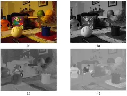
Fig 2.16 illustrates the result of convert color image in RGB domain to image with YUV components. Image (a) is the color image with RGB representation and (b) (c) (d) is YUV components of the image, respectively.
2.4.2
Simulink Implementation
Figure 2.17: Flow chart of RGB2YUV Simulink system
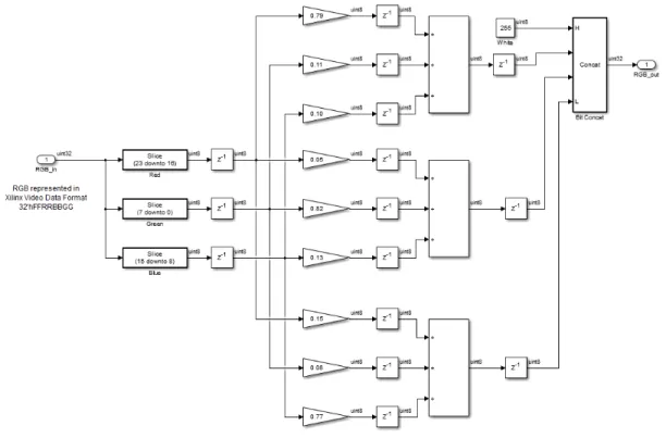
Figure 2.17 gives an overview of the entire RGB2YUV Simulink system. The other blocks are exactly identical with those in color correction model except the RGB2YUV kernel block. The kernel block detail is shown in fig. 2.18. The input bus signal is represented in Xilinx video data format, which is 32’hFFRRBBGG. So we first separate the bus signal to three color components RGB. Red component is bit 23 to 16; Green is bit 7 to 0; Blue is bit 15 to 8. The gain blocks implement multiplication. The sum blocks calculate add and subtract result, which are defined in block parameter. Matrix multiplication is implemented using these gain and sum blocks. Finally the corrected color components are concatenated again to a bus signal. The delay blocks inserted in between will be transferred to registers in hardware, which break down the critical path to achieve higher clock frequency.
Figure 2.18: Implementation of RGB2YUV block in Simulink
Fig 2.19 gives the simulation result in Simulink environment. Image (a) is the color image with RGB representation and (b) (c) (d) is YUV components of the image, respectively.
2.4.3
FPGA Implementation
We validate the entire RGB2YUV design on a KC705 FPGA platform using gener-ated HDL code. The reported maximum frequency is 159.69 MHz. The resources utilization of the RGB to YUV system on FPGA is as follows: 106 slice registers and 286 slice LUTs. Fig. 2.20 illustrates the result of our RGB to YUV system on hardware. Image (a) is the color image with RGB representation and (b) (c) (d) is YUV components of the image, respectively. To display Y(U/V) component in gray scale, we assign the value of signal component to all RGB channels.
(a) (b)
(c) (d)
Figure 2.19: Example of RGB2YUV in Simulink
2.5
Gamma Correction
2.5.1
Introduction
Gamma correction is a nonlinear operation used to adjust pixel luminance in video or still image systems. Image seems bleach out or too dark when it is not properly corrected. Gamma correction controls the overall brightness of an image, crucial for displaying an image accurately on a computer screen.
Gamma correction could be defined by the following power-law expression:
Vout =K×Vinr (2.9)
(a) (b)
(c) (d)
Figure 2.20: Example of RGB2YUV on hardware
common case of K = 1, the inputs and outputs are normalized in the range of [0,1]. For 8-bit grayscale image, the input/output range is between [0,255]. For the case that gamma valuer <1, it is called an encoding gamma; conversely a gamma value
r >1 is called a decoding gamma.
Gamma correction is necessary for image display due to nonlinear property of computer monitor. Almost all computer monitors have an intensity to voltage re-sponse curve which is roughly r = 2.2 power function. When computer monitor is sent a certain pixel of intensity x, it will actually display a pixel with intensity x2.2. This means that the intensity value displayed is less than what it is expected to be. For instance, 0.52.2 = 0.22.
To correct this annoying bug, the input image intensity to the monitor must be gamma corrected. Since the relationship between the voltage sent to monitor and intensity displayed could be depicted by gamma coefficient r and monitor manufac-tures provide the number, we could correct the signal before it reaches the monitor
(a) (b)
(c) (d)
Figure 2.21: Illustration of gamma correction
using a 1r gamma coefficient. The procedure is shown in fig. 2.21. Image (a) is origi-nal video frame; (b)depicts how the image looks like on monitor of gamma coefficient 2.2 without gamma correction. We adjust pixel intensity using a 1r gamma coeffi-cient and get image(c), which looks like image (d) on the monitor with nonlinear property.
If gamma correction is performed perfectly for the display system, the output of monitor correctly reflects the image (voltage) input. Note that monitor systems have many influencing factors, such as brightness and contrast setting other than gamma adjustment. Adjusting monitor display is a comprehensive task.
2.5.2
Simulink Implementation
Figure 2.22 gives an overview of the entire gamma correction Simulink model. The Image From File block, Serialize block, Serialize block and video viewer block are
Figure 2.22: Flow chart of gamma correction system in Simulink
shared with those in previous color correction system. The key block of gamma correction system is 1-D lookup table from hdlsupported library. The gamma curve is described in block parameter as in fig. 2.23.
Figure 2.23: Parameter settings for 1-D Lookup Table
Fig 2.24 gives the gamma correction simulation result in Simulink environment. Image (a) is the the original video frame in grayscale and (b) (c) is the corrected image entering nonlinear computer monitor with gamma coefficient 2.2 and 1.8.
2.5.3
FPGA Implementation
We validate the entire gamma correction design on a KC705 FPGA platform us-ing generated HDL code. The reported maximum frequency is 224.31 MHz. The
(a) (b) (c)
Figure 2.24: Example of gamma correction in Simulink
resources utilization of the gamma correction system on FPGA is as follows: 50 slices, 17 slice flip flops and 95 four input LUTs. Fig. 2.25 illustrates the result of our gamma correction system on hardware. We apply the same gamma correction block on all RGB color channels. Image (a) is the original color image with RGB representation. Image (b) and (c) are the result of gamma correction system of co-efficients 2.2 and 1.8. Image (d) is what the color image looks like on a real monitor with nonlinear property.
2.6
2D FIR Filter
2.6.1
Introduction
The 2D FIR filter is a basic filter for image processing. The output signals of a 2D FIR filter can be computed using the input samples and previously computed output samples as well as filter kernel. For a causal discrete-time FIR filter of order N of 1 dimension, each value of the output sequence is a weighted sum of the most recent input values, as shown in equation (2.10):
(a) (b)
(d) (c)
Figure 2.25: Example of gamma correction on hardware
y[n] =b0x[n] +b1x[n−1] +b2x[n−2] +· · ·+bNx[n−N] (2.10)
where x[n] is the input signal and the y[n] is the output signal. N is the filter order, an Nth order filter has (N+1) terms on the right hand side. bi is the value of
the impulse response at the i-th instant for 0 ≤ i ≤ N of an Nth order FIR filter. For 2-D FIR filter, the output signals rely on both previous pixels of current line and pixels of upper lines. Upon the 2D filter kernel, the 2D FIR filter could be either high-pass filter or low-pass filter. Equation (2.11) and (2.12) gives example of typical high pass filter kernel and low pass filter kernel.
HighP ass= [ 0 −1 0 −1 4 −1 0 −1 0 ] (2.11) LowP ass= [ 1/16 1/8 1/16 1/8 1/4 1/8 1/16 1/8 1/16 ] (2.12) (a) (b) (c) (d)
Figure 2.26: Illustration of 2D FIR filter
In this chapter, we will take low pass filter for example. Fig 2.26 illustrates the result of low pass filter using different filter kernel. Image (a) is the original image and (b) (c) (d) is the filtered image, respectively.
Figure 2.27: Flow chart of 2D FIR filter system in Simulink
2.6.2
Simulink Implementation
Figure 2.27 gives an overview of the entire 2D FIR filter Simulink system. The architecture is also shared with following 2D filters in this chapter. The filtering block is the only difference. Other blocks are the very same ones.
Figure 2.28: Flow chart of 2D FIR filter block in Simulink
Sobel filter block is implemented as fig. 2.28. We design a Sobel kernel block to calculate the filter response of input image, then calculate the response absolute value and convert it to uint8 data type for further display.
Fig. 2.29 is the architecture of Sobel kernel block. The 2D FIR algorithm maintains three line buffers. Each iteration the input pixel is pushed into the current line buffer that is being written to. The control logic rotates between these three buffers when it reaches the column boundary. Each buffer is followed by a shift register and data at the current column index is pushed into the shift register. At each iteration a 3x3 kernel of pixels are formed from the pixel input, shift registers
Figure 2.29: Flow chart of Sobel Kernel block
and line buffer outputs. The kernel are multiplied by a 3x3 filter coefficient mask and the sum of the result values is computed as the pixel output as in figure 2.30.
Figure 2.30: Architecture of kernel mult block
Fig 2.31 gives the low pass 2D FIR filter result in Simulink environment. Image (a) is the the original video frame in grayscale and (b) is smoothed image output using low pass filter in equation (2.12).
(a) (b)
Figure 2.31: Example of 2D FIR filter in Simulink
2.6.3
FPGA Implementation
(a) (b) (c)
Figure 2.32: Example of 2D FIR filter on hardware
We validate the entire 2D FIR filter design on a KC705 FPGA platform using generated HDL code. The reported maximum frequency is 324.45 MHz. The re-sources utilization of the 2D FIR filter system on FPGA is as follows: 71 slices, 120 flip flops, 88 four input LUTs and 1 FIFO16/RAM16. Fig. 2.32 illustrates the 2D FIR filter system on hardware. Image (a) is the color image in grayscale and (b) (c) is blurred image using different kinds of low pass filter kernels.
2.7
Median Filter
2.7.1
Introduction
Median filter is a nonlinear digital filtering technique, usually used for removing the noise on an image. It is a more robust method than the traditional linear filtering in some circumstances. The noise reduction is an important pre-processing step to improve the results of the later process. The main idea of median filter is that using a sliding window scan the whole image and replaces the center value in the window with the median of all the pixel values in the window. The input image for median filter is the grayscale image and the window is replied to each pixel of it. Usually, we choose the window size as 3 by 3. Here we give an example of how the median filter work in one window. For example, we have a 3× 3 pixel window from an image. The pixel values in the image window are 122, 116, 141, 119, 130, 125, 122, 120, 117. We can calculate what is the median value from the central one and all the neighborhood values. The median value is 120. So the next step is to replace the central value with the median value 120.
Compared to basic median filter, adaptive median filter may be more pratical. In adaptive median filter, we just do the central value - median value swap when the central value is black (0) or white (255) pixel. Otherwise, the system will keep the original central pixel intensity.
Fig 2.33 illustrates the result of median filter using different sizes of filter kernel. Image (a) is the original image; image (b) is image (a) with thin salt and pepper noise; image (c) is the result of 3×3 median filter applied on image (b); image (d) is image (a) with thick salt and pepper noise; image (e) is the result of 3×3 median filter applied on image (d); image (f) is the result of 5×5 median filter applied on image (d). Comparing those images, we can find that the median filter blurs
(a) (b) (c)
(d) (e) (f)
Figure 2.33: Illustration of median filter
input image. With larger median filter mask, we filter out more noise, but lose more information as well.
2.7.2
Simulink Implementation
The architecture of median filter Simulink system is the same with 2D FIR filter model in fig. 2.27. The median filter is depicted in fig. 2.34. The median algorithm, like 2D FIR filter, also maintains three line buffers. Each iteration the input pixel is pushed into the current line buffer that is being written to. The control logic rotates between these three buffers when it reaches the column boundary. Each buffer is followed by a shift register and data at the current column index is pushed into the shift register. At each iteration a 3x3 kernel of pixels are formed from the pixel input, shift registers and line buffer outputs. Then the median block decide the median output. Note that our adaptive median filter is design to filter out salt
Figure 2.34: Flow chart of median filter block in Simulink
and pepper noise. It should be modified in order to handle other kinds of error. It first chooses the median intensity of input 9 input pixels in compare block in fig. 2.35, then compares the current pixel intensity with 0 and 255. If the pixel is salt or pepper, the switch block chooses median value as output; otherwise it just passes through current pixel intensity.
Figure 2.35: Flow chart of the median Simulink block
Figure 2.36: Architecture of the compare block in Simulink
Figure 2.37: Implementation of basic compare block in Simulink
compare blocks as in fig. 2.37. The basic compare blocks, taking 2 data input, employ 2 relational operators and 2 switches to get the larger one and smaller one. With such design, we get the median pixel value of 9 input pixels.
Fig 2.38 gives the median filter result in Simulink environment. Image (a) and (c) is the the original video frame in different density of salt and pepper noise. Image(b) and (d) is the recovered images using our 3×3 median filter block.
(a) (b)
(c) (d)
Figure 2.38: Example of median filter in Simulink
2.7.3
FPGA Implementation
We validate the entire adaptive median filter design on the KC705 FPGA platform using generated HDL code. The reported maximum frequency is 374.92 MHz. The resources utilization of the median filter system on FPGA is as follows: 81 slices, 365 slice LUTs and 1 Block RAM/FIFO. Fig. 2.39 illustrates the median filter system on hardware. Image (a) and (b) are the original grayscale image and image with salt and pepper noise. Image (c) is recovered image using generated RTL median filter.
(a) (b) (c)
Figure 2.39: Example of median filter on hardware
2.8
Sobel Filter
2.8.1
Introduction
The Sobel operator performs a 2-D spatial gradient measurement on an image and so emphasizes regions of high frequency that correspond to edges. Typically it is used to find the approximate absolute gradient magnitude at each point in an input grayscale image. Here we also need a window to do the scanning work and here we still choose 3 by 3 as the size of the window, then we apply two kernels on the sliding window separately and independently. The x directional kernel is shown as the following equation:
Gx = 0.125 0 −0.125 0.25 0 −0.25 0.125 0 −0.125
and y directional kernel is similar. By summing up the x and y directional kernel response, we get the final Sobel filter response.
(a) (b)
Figure 2.40: Illustration of Sobel filter output image (b) is highlighted result using Sobel filter;
2.8.2
Simulink Implementation
Figure 2.41: Flow chart of Sobel filter block in Simulink
The architecture of Sobel filter Simulink system is the same with 2D FIR filter system in fig. 2.27. The Sobel filter block filter is depicted in fig. 2.41. It first calculates Sobel filter response in x and y direction in Sobel kernel block, then sum their absolute values to get the final Sobel filter response and quantize the response to Uint8 type for following display.
Figure 2.42: Flow chart of the Sobel kernel block in Simulink
Figure 2.42 shows the implementation of Sobel kernel block. Each iteration the input pixel is pushed into the current line buffer. The control logic rotates between these three buffers when it reaches the column boundary. Each buffer is followed by a shift register and data at the current column index is pushed into the shift register. At each iteration a 3x3 surrounding of pixels are formed from the pixel input, shift registers and line buffer outputs. Then the x/y directional block in fig. 2.43 takes the surrounding pixels to calculate Sobel filter response in 2 orthometric directions.
Fig 2.44 gives the Sobel filter result in Simulink environment. Image (a) is the the original video frame. Image(b) is the gradient grayscale images using our Sobel filter Simulink block.
2.8.3
FPGA Implementation
We validate the Sobel filter design on the KC705 FPGA platform using generated HDL code. The reported maximum frequency is 227.43 MHz. The resources utiliza-tion of the Sobel filter system on FPGA is as follows: 156 slices, 167 slice LUTs and
Figure 2.43: Flow chart of the x/y directional block in Sobel filter system 1 Block RAM/FIFO. Fig. 2.45 illustrates the Sobel filter system on hardware. Im-age (a) is the original grayscale image and (b) is sharpened image with Sobel filter, which highlights all the edges containing most critical information of the image.
2.9
Grayscale to Binary Image
2.9.1
Introduction
Converting grayscale image to binary image is often used in order to find Region of Interest - a portion of image that is of interest for further processing because binary image processing reduces the computational complexity. For example, Hough transform is widely used to detect straight lines, circle and other specific curve in an image and it takes only binary image input.
Grayscale image to binary image conversion always follows a high pass filter, such as Sobel filter, to highlight the key information of an image, which is always boundary of object. Subsequently, the key step of grayscale to binary conversion is to set up an threshold. Each pixel of gradient image generated by highpass filter is
(a) (b)
Figure 2.44: Example of Sobel filter in Simulink
(a) (b)
Figure 2.45: Example of Sobel filter on hardware
compared to the chosen threshold. If the pixel intensity is larger than the threshold, it is set to 1 in the binary image. Otherwise, it is set to 0.
We could imagine an appropriate threshold determine the quality of converted binary image. Unfortunately, there isn’t a single threshold working for every image. A threshold good for bright scene could never work for dark scene, and vice versa. In section 3.1.2, we introduce an adaptive thresholding method to convert grayscale image to binary image. Here, we will focus on fixed threshold method.
dif-(b)
(d)
(a) (c)
(e)
Figure 2.46: Illustration of grayscale to binary image conversion
ferent threshold values. Image (a) is the original image; image (b) is the gradient of image (a) from Sobel filter; image (c) (d)(e) are corresponding binary image using different threshold values. We could easily find that the result keeps more image information with lower threshold. But low threshold also remains more noises. And vice versa.
2.9.2
Simulink Implementation
Fig. 2.47 gives an overlook of grayscale to binary image conversion system in Simulink. To keep critical edge information and dismiss noises, we first employ Sobel filter to highlight object boundary in image. The key operation of grayscale to binary image conversion is comparison. Here we use a compare to constant block to compare pixel intensity of Sobel filter output with a pre-defined constant as figure
Figure 2.47: Flow chart of the proposed grayscale to binary image conversion sys-tems
2.48. This will produce an output a binary image of 1 (white) and 0 (black).
Figure 2.48: Implementation of the gray2bin block in Simulink
(a) (b) (c)
Figure 2.49: Example of grayscale to binary image conversion in Simulink
Fig 2.49 gives the grayscale to binary image conversion result in Simulink envi-ronment. Image (a) is the original grayscale image; image (b) is high-passed image using Sobel filter; image (c) is converted binary representation of image content.
(a) (b)
Figure 2.50: Example of grayscale to binary image conversion on hardware
2.9.3
FPGA Implementation
We validate the grayscale to binary conversion design on the KC705 FPGA platform using generated HDL code. The reported maximum frequency is 426.13 MHz. The resources utilization of the grayscale to binary system on FPGA is as follows: 9 slices registers and 2 slice LUTs. Fig. 2.50 illustrates the grayscale to binary system on hardware. Image (a) is the original grayscale image; image (b) is corresponding binary image, which keeps the main information of original grayscale image.
2.10
Binary/Morphological Image Processing
2.10.1
Introduction
Morphological image processing is a collection of non-linear operations related to the shape or morphology of features in an image. Morphological technique typically probes a binary image with a small shape or template known as structuring ele-ment consisting of only 0’s and 1’s. The structuring eleele-ment could be any size and positioned at any possible locations in the image.
The mostly used structuring elements are square and diamond as (2.13) and (2.14). SquarSE = 1 1 1 1 1 1 1 1 1 (2.13) DiamondSE= 0 1 0 1 0 1 0 1 0 (2.14)
In this section, we define two fundamental morphological operation on binary image: dilation and erosion. Dilation compares the structuring element with the corresponding neighborhood of pixels to test whether the elements hits or intersects with the neighborhood. Erosion operation compares the structuring element with the corresponding neighborhood of pixels to determine whether the elements fits within the neighborhood of pixels. In other words, dilation operation set the value of output pixels as 1 if any of the pixels in the input pixel’s neighborhood defined by the structuring element; the value of output pixel is set to 0 if any of the neighborhood pixels value are 0 in erosion operation. Erosion operation set the value of output pixels as 1 only if all of the pixels in the input pixel’s neighborhood defined by the structuring element; otherwise the value is set to 0;
Here we take the image dilation as example. Fig 2.51 illustrates the result of image dilation using different structuring elements. Image (a) is the original image; image (b) is the dilation result with structuring element in (2.13); image (c) is the dilation result with structuring element in (2.14); image (d) is the dilation result with 11×1 vector structuring element.
(a) (b)
(c) (d)
Figure 2.51: Illustration of morphological image processing
2.10.2
Simulink Implementation
Fig. 2.52 gives an overlook of image dilation block in Simulink. The delay blocks collect current pixel surroundings (according to structuring element) for bit opera-tion blocks to perform subsequent calculaopera-tion. The key operaopera-tion of binary image morphology is bit operation. For image erosion application, bits AND operation is preformed; for image dilation application, we need to perform bits OR operation. For example, a 5-input OR operation is applied to perform image dilation in fig. 2.53.
Fig 2.54 gives the image dilation result in Simulink environment. Image (a) is the original binary image; image (b) is dilated image output using 3×3 square structuring element.
Figure 2.52: Flow chart of the proposed image dilation block
Figure 2.53: Detail of the bit operation block
2.10.3
FPGA Implementation
We validate the image dilation design on the KC705 FPGA platform using gener-ated HDL code. The reported maximum frequency is 359.02 MHz. The resources utilization of the image dilation system on FPGA is as follows: 28 slice registers, 32 slice LUTs and 1 Block RAM/FIFO. Fig. 2.55 illustrates the image dilation system on hardware. Image (a) is the original binary image and (b) is dilated image using generated image dilation HDL code.
(a) (b)
Figure 2.54: Example of image dilation in Simulink
(a) (b)
Figure 2.55: Example of image dilation on hardware
2.11
Summary
In this chapter, we introduce basic image/video processing blocks in Simulink and on hardware. Because implementation of video/image processing blocks on hardware is time consuming, not to mention debugging, we first prototype and implement these blocks in Simulink and then transfer the design to RTL implementation using HDL coder toolbox product. Finally, the RTL design is validated on Xilinx KC705 development platform.
Chapter 3
Advanced Video/Image Processing
3.1
Lane Departure warning system
3.1.1
Introduction
Each year millions of traffic accidents occurred around the world cause loss of lives and properties. Improving road safety through advanced computing and sensor technologies has drawn lots of interests from the auto industry. Advanced Driver assistance system (ADAS) thus gains great popularity, which helps drivers to prop-erly handle different driving condition and giving warnings if any danger is insight. Typical driver assistance system includes, but is not limited to, lane departure warning, traffic sign detection [1], obstacle detection [2], pedestrian detection [3], etc. Many accidents were caused by careless or drowsy drivers, who failed to notice that their cars were drifting to neighboring lanes or were too close to the car in the front. Therefore, lane departure warning (LDW) system and front collision warning (FCW) system are designed to prevent this type of accidents.
Different methods have been proposed for lane keeping and front vehicle detec-tion. Marzotto et al. [4] proposed a RANSAC-like approach to minimize
computa-tional and memory cost. Risack et al. [5] used a lane state model for lane detection and evaluated lane keeping performance as a parameter called time to line cross-ing (TLC). McCall et al. [6] proposed a ’video-based lane estimation and trackcross-ing’ (VioLET) system which uses steerable filters to detect the lane marks. Others used Hough transform for feature based lane detection. Wang et al. [7] combined Hough transform and Otsu’s threshold method together to improve the performance of lane detection and implemented it on a Kintex FPGA platform. Lee et al. [8] removed redundant operations and proposed an optimized Hough transform design which uses fewer logic gates and less number of cycles when implemented on an FPGA board. Lin et al. [9] integrated lane departure warning system and front collision warning system on a DSP board.
The key requirements of a driver assistance system are rapid processing time and low power consumption. We consider FPGA as the most appropriate platform for such a task. Owing to the parallel architecture, an FPGA can perform high-speed video processing such that it can issue warnings timely and provide drivers more time to response. Besides, the cost and power consumption of modern FPGAs, particularly small size FPGAs, are considerably efficient.
In this contribution, we present a monocular vision lane departure warning and front collision warning system jointly implemented on a single FPGA device. Our experimental results demonstrate that the FPGA-based design is fully functional and it achieves the real-time performance of 160 frame-per-second (fps) for high resolution 720P video.
3.1.2
Approaches to Lane Departure Warning
The proposed LDW and FCW system takes video input from a single camera mounted on a car windshield. Fig. 3.1 shows the flow chart of the proposed LDW
Sobel Filter Otsu Threshold Binarization Hough Transform Lane Detection Departure Lane Departure Warning Gradient Image Binary Image Peak T Shadow Detection Distance Calculation LUT Collision Front Collision Warning With Velocity T Image Dilation Grayscale Image
Figure 3.1: Flow chart of the proposed LDW and FCW systems
and FCW systems. The first step is to apply a Sobel filter on the gray scale image frame to sharpen the edges after an RGB to gray scale conversion. This operation helps highlight the lane marks and front vehicle boundary while eliminating dirty noise on the road. The operator of Sobel filter is
G=G2x+G2y (3.1)
where the Gx is Sobel kernel in x- direction as in (3.2) and similarly Gy in y
-direction. Gx = 0.125 0 −0.125 0.25 0 −0.25 0.125 0 −0.125 (3.2)
Next, an important task is to convert the gray scale video frame to a “perfect” binary image which is used by both LDW and FCW systems. A “perfect” binary
image means high signal-to-noise ratio, preserving desired information while aban-doning useless data to produce more accurate results and to ease computational burden. For LDW and FCW systems, the desired information is lane marks of the road and vehicles in the front. Therefore, we cut off the top part of every image and crop the area of interest to the bottom 320 rows of a 720P picture. All subse-quent calculations are conducted on this region of interest (ROI). When converting from gray scale to binary image, a fixed threshold is often not effective since the illumination variance has apparent influence on the binarization. Instead, we choose Otsu’s threshold, a dynamic and adaptive method, to obtain binary image that is insensitive to background changes. The first step of Otsu’s method is to calculate probability distribution of each gray level as in (3.3).
pi =ni/N (3.3)
where pi and ni are probability and pixel number of gray level i. N is the total
pixel number of all possible levels (from 0 to 255 for gray scale). The second is to step through all possible level t to calculate ω∗(t) and µ∗(t) as in (3.4) and (3.5).
ω∗(t) = t X i=0 pi (3.4) µ∗(t) = t X i=0 ipi (3.5)
The final step is to calculate between-class variance (σ∗B(t))2 as in (3.6).
(σB∗ (t))2 = [µ
∗
Tω
∗(t)−µ∗(t)]2
ω∗(t)×[1−ω∗(t)] (3.6)
re-written as (3.7)
σB2 (t) = [µT/N×ω(t)−µ(t)]
2
ω(t)×[N −ω(t)] (3.7)
whereω(t) = ω∗(t)×N andµ(t) =µ∗(t)×N. Otsu’s method selects levelt∗ as binarization threshold, which has largest σ2
B(t
∗). Fig. 3.2 illustrates effects of Sobel
filter and Otsu’s threshold binarization.
(a)
(b)
(c)
Figure 3.2: Illustration of Sobel filter and Otsu’s threshold binarization. (a) is the original image captured from camera. (b) and (c) are ROI after Sobel filtering and binarization, respectively
Image dilation is a basic morphology operation. It usually uses a structuring element for probing and expanding shapes in a binary image. In this design, we apply image dilation to smooth toothed edges introduced by Sobel filter, which can
Figure 3.3: Hough transform from 2D space to Hough space assist the subsequent operations to perform better.
Furthermore, Hough transform (HT) is widely used as a proficient way of finding lines and curves in binary image. Since most lines on a road are almost straight in pictures, we mainly discuss the way of finding straight lines in binary image using Hough transform. Every point (x,y) in 2D space can be represented in polar coordinate system as
ρ=xcos(θ) +ysin(θ) (3.8)
Fig. 3.3 illustrates 2D space to Hough space mapping. If point A and B are on the same straight line, there exists a pair of ρ and θ that satisfy both equation, which means two curves in polar coordinate have an intersection point. As more points on the same line are added to the polar system, there should be one shared intersection point between these curves. In Hough transform algorithm, it keeps track of all intersection points between curves and the intersections with big voting imply that there is a straight line in 2D space.
By analyzing Hough transform for lane detection, we optimize the transform during the following two steps: 1) dividing the image into a left part and a right part, perform HT with positive θ for the left part and negative θ for the right part due to the slope nature of the lanes; 2) further shrink the range of θ by ignoring
those lines that are almost horizontal with θ near ±90. Empirically, the range of
θ is set to [1,65] for the left part and [−65,−1] for the right part. We choose the most voted (ρ, θ) pairs of left part and right part as detected left lane and right lane, respectively. To avoid occasional errors on a single frame, the detected lanes are compared with results from preceded 4 frames. If they are outliers, the system takes weighted average of results of preceded 4 frames as the current frame’s lanes. If either the left lane or the right lane is excessively upright (i.e. abs(θ)<30), the system issues lane departure warning.
For the front collision warning system, we identify the front vehicle by detecting the shadow area within a triangular region in front of the car on the binary image. From the position of the front vehicle, the actual distance is obtained using an empirical look-up-table (LUT). The system generates a collision warning signal when the distance is smaller than suggested safe distance at the vehicle traveling speed.
3.1.3
Hardware Implementation
In this section, we elaborate the hardware architecture for LDW and FCW systems, especially for the design implementations of Sobel filter, Otsu’s threshold binariza-tion, Hough transform and front vehicle detection.
Fig. 3.4 is the architecture of Sobel filter. The Sobel filter module takes 3 Block RAMs (BRAMs) to store the current row of input pixels and buffer 2 rows right above it. Two registers connected to Block RAM output buffer the read data for 2 clock cycles (cc) for each row. With such an architecture, we get every pixel together with its 8 neighbors at the same cc. The Sobel kernel is then applied on the 3×3 image block. The system sums the 3×3 result to get Sobel response in x- and y -directions. The sum of square of Sobel filter response in two directions is set as gradient value of the center pixel (the red color in Fig. 3.4). The image dilation
... ... ... ... ... ... X Line Buffer Block RAM
Sobel kernel Reg
=
Figure 3.4: Sobel filter architecture
module has similar architecture as Sobel filter. The only difference is that it uses a structuring element of 3×3 1’s rather than Sobel kernel on the block and produces a dilated binary image.
REG REG REG REG REG Gray level w RAM u RAM REG X + REG + REG X 1/N X - X X i ut Deno reg Nume X -N X Nume reg Deno COMP
Figure 3.5: Datapath for Otsu’s threshold calculation
We implement the Otsu’s method by closely following (3.7). The gradient pixel intensity is 8-bit gray level as an input of this block. Hence we use 256 registers to count the total number of every level (i.e. ni) in ROI of current video frame. The
following step is to accumulate ni and i×ni to getω andµ, which are stored in two
separate RAMs. [10] directly computes σ2B as in (6), but the division is expensive in term of processing speed and hardware resource use. [7] takes advantage of extra ROMs to convert division to subtraction in log domain. After careful consideration,
we find that this part is to find the intensity level that maximizes σB2 rather than get the exact value of σ2B. Therefore, we design a datapath to find the Otsu’s threshold as in Fig. 3.5. As t varies from 0 to 255, ω(t) and µ(t) are read from the RAMs to calculate the numerator and the denominator of σ2
B(t). Two registers,
Numerator reg and Denominator reg buffer the corresponding numbers of biggest
σ2
B(i) for i < t. Just two multipliers and one comparator are deployed to check
if σ2
B(t) is larger than the largest σB2 (i) for i < t. If so, the Numerator reg and
Denominator reg are updated accordingly. With such an architecture, we find the Otsu’s threshold that is employed to convert the gradient gray-level image to black and white image.
ROM1 X ROM2 X 5 COSINEs 5 SINEs x y +
RAM1 RAM2 RAM3 RAM4 RAM5
ρ
Control Logic count count
address address address address address
Figure 3.6: Hough transform architecture
The Hough transform is the most computationally expensive block in the entire design. Here we just discuss Hough transform for the left part since the right part has almost identical architecture. As mentioned in Section II, we let θ vary across 1 to 65 to find the left and right lanes by seeking most voted (ρ, θ) pairs. It is reasonable to assume less than 10% pixels are edge pixels in a road scene. Thus, in order to achieve real-time Hough transform, we propose a pipeline and dedicated
architecture as in Fig. 3.6. ROM1 and ROM2 store cosine and sine values for θ
from 1 to 65 (totally 13 groups with every 5 successive ones as a group). When the HT module receives position information of edge pixels, it reads out cosine and sine values ofθand performs Hough transform. Control logic generates a signalcount to indicate which 5 θ0sare being processed. Once they receives the ρ, each block reads its corresponding value from RAMs, adds it by 1, and then write it back. After all edge pixels go through the Hough transform module, the system scans all RAM locations and finds most voted (ρ, θ) pair as the left lane. If the detected lanes are excessively upright (θ < 30), a lane departure warning will be released at the very first time. Control logic Binary image RAM Accumulator Comparator Search logic ROM Y X Left position right position Total length Shadow length Vehicle location Distance Candidate
Figure 3.7: Flow chart of front vehicle detection
Fig. 3.7 shows the algorithm flow chart for detecting front vehicles. The de-tection is based on shadow information in a triangular region formed by the left and right lanes. When a binary image enters, the control logic generates position
information X and Y. For every row, the RAM, as a LUT, provides left and right boundary positions of a targeted triangle region based on vertical information Y. The Accumulator block counts the white pixels within the triangle area for each row. If the number of filled pixels is larger than a fixed ratio to the triangle width of that row, it is a candidate for front vehicle detection. The candidate row, which are closest to the bottom of an image, is considered as the front vehicle’s position. Finally, the system converts the row number to the physical distance on the ground through a LUT implemented using a ROM. If the vehicle traveling speed is known, a front collision warning can be issued when the front vehicle is closer than the safe distance.
3.1.4
Experimental Results
The proposed design is implemented in Verilog HDL. Xilinx ISE tool is used for design synthesis, translation, mapping and placement and routing (PAR). In order to validate the entire design, we conduct an experiment on a KC705 FPGA platform. The video streams from a camera mounted on a vehicle windshield are sent to an on-board Kintex-7 FPGA via FMC module. The FPGA performs lane departure and front collision warning examination on every video frame and exports the results to a monitor for display. The input video is 720P resolution at the rate of 60 fps. We take the video clock as system clock of our design, which is 74.25MHz in this case.
Table 3.1: Device utilization summary
Resources Used Available Utilization
Number of Slices Registers: 8,405 407,600 2%
Number of Slice LUTs: 10,081 203,800 4%
Number of Block RAMs: 60 445 13%
The resources utilization of the LDW and FCW systems on an XC7K325TFPGA is shown in Table 3.1. Although we verify the design on a 7-series FPGA, it can also be implemented on a much smaller device for lower cost and less power consumption, e.g. Spartan-6 FPGA. The reported maximum frequency is 206 MHz. Thus if the system runs at maximum frequency, it can process 720P video at 160 fps, which is corresponding to the pixel clock frequency at 206 MHz. The design is validated by road tests using the FPGA-based hardware system. Fig. 3.8 illustrates some results of our LDW and FCW systems. The detected lanes are marked as green and the detected front vehicle is marked as blue.
(a)
(b)
(c)
(d)
3.2
Traffic Sign Detection System Using SURF
3.2.1
Introduction
In driver-assistance systems, traffic sign detection is among the most important and helpful functionalities. Many traffic accidents happen due to drivers’ failure to ob-serve the road traffic signs, such as stop signs, do not enter signs, speed limit signs, and etc. Three kinds of methods are often applied to implement road traffic sign de-tection – color-based, shape-and-partition-based, and feature-based algorithms[11]. Traffic signs are designed with unnatural color and shape, making them conspic-uous and well-marked. Color-based and shape-based method are the initial and straightforward ones to be used for sign detection[12][13]. However, these methods are sensitive to the video environment. Illumination change and partial occlusion of traffic sign seriously degrade the effectiveness of these methods. The third type of methods are based on feature extraction and description. These algorithms detect and describe salient blob as features of an image and video. The features are usually unaffected by the variance of illumination, position and partial occlusion. Reported feature-based algorithms contain Scale Invariant Feature Transformation (SIFT)[14], Histogram of Oriented Gradient (HoG)[15], Haar-like feature algorithm[16], etc.
Speeded Up Robust Features (SURF) [17] is one of the best feature-based algo-rithms and has found wide application in the Computer Vision community[18][19][20]. It extracts Hessian matrix-based interest points and has a distribution-based de-scriptor, which is a scale- and rotation-invariant algorithm. These features make it perfect for object matching and detection. The key advantage of SURF is to use integral image and Hessian matrix determinant for feature detection and descrip-tion, which greatly boosts the process efficiency. Even so, like other feature-based algorithms, SURF is computationally complex which often results very low frame
rate on an embedded processor. In order to employ SURF for real-time appli-cations, parallel processing architecture and platform need to be considered. By analyzing the parallelism during each step of the SURF algorithm, we choose Field Programmable Gate Array (FPGA) as the embedded platform because of its rich resource