Ballistic rectification of vortex domain wall chirality at nanowire corners
K.Omari,1R. C.Bradley,1T. J.Broomhall,1M. P. P.Hodges,1M. C.Rosamond,2 E. H.Linfield,2M.-Y.Im,3,4P.Fischer,5,6and T. J.Hayward1
1
Department of Materials Science and Engineering, University of Sheffield, Sheffield S1 3JD, United Kingdom
2
School of Electronic and Electrical Engineering, University of Leeds, Leeds LS2 9JT, United Kingdom
3
Center for X-Ray Optics, Lawrence Berkeley National Laboratory, Berkeley, California 94720, USA
4
Daegu Gyeongbuk Institute of Science and Technology, Daegu 711-873, South Korea
5
Materials Sciences Division, Lawrence Berkley National Laboratory, Berkeley, California 94720, USA
6
Department of Physics, University of California, Santa Cruz, California 94056, USA
(Received 3 September 2015; accepted 13 November 2015; published online 2 December 2015)
The interactions of vortex domain walls with corners in planar magnetic nanowires are probed using magnetic soft X-ray transmission microscopy. We show that when the domain walls are propagated into sharp corners using applied magnetic fields above a critical value, their chiralities are rectified to either clockwise or anticlockwise circulation depending on whether the corners turn left or right. Single-shot focused magneto-optic Kerr effect measurements are then used to demon-strate how, when combined with modes of domain propagation that conserve vortex chirality, this allows us to dramatically reduce the stochasticity of domain pinning at artificial defect sites. Our results provide a tool for controlling domain wall chirality and pinning behavior both in further ex-perimental studies and in future domain wall-based memory, logic and sensor technologies.VC 2015 AIP Publishing LLC. [http://dx.doi.org/10.1063/1.4936565]
Devices based on the motion of domain walls (DWs) in magnetic nanowires have been in development for over a decade.1–3While simple descriptions visualize DWs as rigid particles, DWs actually have complex internal magnetization structures4 that change dynamically as they propagate.5–7 Key to understanding DW structure is the concept of chiral-ity, which describes the sense of magnetization rotation across the DW. For example, in the case of vortex DWs (VDWs), chirality dictates whether their internal magnetiza-tion rotates clockwise (CW) or anticlockwise (ACW) around a central out-of-plane core.
Chirality has a strong influence on DW behavior: VDWs with opposite chiralities pin differently at notches, resulting in stochastic depinning field distributions in systems where chirality is ill-defined.8,9Furthermore, chirality dictates the paths of DWs in branched nanowires, and therefore the ge-ometry of Dirac strings in artificial spin-ice lattices.10In sys-tems where DW structure can be stabilized, chirality also offers a binary degree of freedom, leading to proposals for chirality-based logic networks.11
DWs injected using injection pads or current lines have random chiralities, leading to uncontrolled pinning behav-iors. However, by breaking the symmetry of these features, chirality can be controlled at the point of injection.10,12 Controlling and manipulating chiralities during propagation is more challenging, but can be achieved by interacting DWs with orthogonal nanowire sections,13large notches,14or end-domains;15however, these approaches all involve the intro-duction of large defects into the nanowires. Pulsed rotating fields can be used to select DW chirality in ring-shaped nanowires,16but this approach would be complex to imple-ment in devices.
In this paper, we propose a simple method of controlling DW chirality in continuous nanowires. We show that DWs propagated ballistically into sharp nanowire corners are
reliably rectified to either CW or ACW chirality depending on whether the corner turns left or right. We then demon-strate how this approach can be exploited to dramatically reduce the stochasticity of pinning at artificial defect sites.
To probe the interaction of VDWs with corners we fab-ricated 400 nm wide nanowires, with geometries similar to that shown in Fig.1(a), on Si3N4membranes using electron
beam lithography with lift-off processing. Metallization with 40 nm of Ni80Fe20 was achieved by thermal evaporation.
DWs were injected from the pads at the nanowires’ left ends and propagated into corners with radii, r¼1lm, 2lm, or 5lm using applied magnetic fields. Nanowires with corners that turned both left (UP geometry) and right (DOWN geom-etry) were investigated. In some nanowires, a symmetrical double-notch with gap-size “g” was positioned before the corner to allow the initial chiralities of the DWs to be probed. To measure the VDWs’ chiralities, we performed magnetic transmission soft X-ray microscopy (MTXM) experiments using beamline 6.1.2 at the Advanced Light Source, which provided spatial resolution<25 nm.
We performed initial measurements on both UP and DOWN geometry nanowires with r¼1lm and g¼160 nm. The nanowires were first saturated into continuous configura-tions before Hx¼150–180 Oe was applied to inject
head-to-head (H2H) VDWs from the pads and move them to the notches. The applied field was then removed to relax the VDWs and allow their chiralities to be determined. We then applied Hx¼300–350 Oe to depin the VDWs from the
notches and propagate them into the vertical sections of the nanowires beyond the corners, before the field was removed again to determine the VDWs’ final chiralities.
Figs. 1(b)–1(d) present the results of these measure-ments. For the UP nanowires, VDWs with CW chirality were always observed after the corner, no matter whether the injected DWs had CW (Fig. 1(b)) or ACW (Fig. 1(c))
chirality. Conversely, for the DOWN nanowires, only DWs with ACW chirality were observed after the corner (Figs.
1(d)and1(e)). Together, these results indicated that the cor-ners had a strong rectifying effect on the chirality of the DWs. The above trends were observed consistently over a total of 28 imaging cycles of the two nanowire geometries (for full details, see Ref.17), allowing us to reject the hy-pothesis that the output chirality was random at a significant level of 5%. Furthermore, the DWs’ chirality flipped in nine
events allowing us to reject the hypothesis that the rectifica-tion probability was less than 70%.
To gain a deeper understanding of the rectification process, we performed micromagnetic simulations of ACW and CW DWs passing through r¼1lm corners in UP geome-try nanowires using the OOMMF software package.18 Simulations were performed on a 4 nm4 nm40 nm mesh using standard values for the material properties of Ni80Fe20:
saturation magnetization, Ms¼860 kA/m, exchange stiffness,
Aex¼13 pJ/m, magnetocrystalline anisotropy constant,
K1¼0 and damping constant, and a¼0.02. While
approxi-mating the nanowire as a 2D mesh was expected to make minor modifications to the details of the DW dynamics, this approach reduced computation time, while still allowing the basic rectification process to be understood. Initial H2H VDW structures were propagated into the corners by applyingþHx.
Based on the experimental results, it was expected that ACW VDWs would be rectified to CW chirality, while CW VDWs would pass through the corner unchanged.
We initially performed simulations with a low propaga-tion field of Hx¼50 Oe to avoid turbulent DW dynamics.
7
This was above the Walker breakdown (WB) field,5 but within the oscillatory regime of DW motion6where dynam-ics were periodic, and, as we will show later, conserve vortex chirality in this nanowire geometry. Figs.2(a)and2(b) com-pare the simulated dynamics of DWs with CW and ACW chiralities as they were propagated into the corner. The CW VDW passed through without changing its chirality, while the ACW VDW was rectified to CW chirality, in good agree-ment with the MTXM results.
Detailed examination of the simulations revealed the cause of the rectifying effect: In the case of the CW VDW, the magnetization in the leading edge of the VDW pointed alongy, parallel to that of the vertical section of the nano-wire beyond the corner, allowing it to pass through easily. Conversely, for the ACW VDW, the magnetization in the leading edge was alongþy, antiparallel to the magnetization in the vertical section. As the DW approached the corner this produced a frustrated and unstable region of magnetization in front of it, allowing the nucleation of a CW vortex core at 10.2 ns (indicated by a blue arrow in the inset of Fig.2(a)). As the DW moved further around the corner, the CW vortex core moved towards the center of the nanowire, while the original ACW core annihilated at the nanowire’s upper edge, completing the rectification process.
Figures2(c)and2(d)present equivalent simulations for Hx¼250 Oe, a field closer to that required to depin the DWs
in the experimental measurements. Here, the dynamics were turbulent, with the DWs becoming extended and containing large numbers of vortex/antivortex cores at any given instant. Nevertheless, the rectification process still occurred, with both DWs resolving into CW VDW structure as they passed into the vertical section of nanowire. Clearly, the magnetiza-tion in the vertical secmagnetiza-tion was able to bias the final nuclea-tion events towards CW chirality as the DWs resolved into stable VDW configurations.
The mechanism we propose above explains why moving from the UP to the DOWN geometry nanowires caused recti-fication to ACW rather than CW chirality (Figs. 1(d) and
1(e)): in the DOWN geometry, the vertical section of
[image:2.612.57.293.54.561.2]nanowire was magnetized alongþy rather thany and would align with leading edge of a ACW VDW, causing rectification to that chirality. Following this logic, changing from H2H to tail-to-tail (T2T) DWs should also switch the nature of the rectification, and this is demonstrated for an UP geometry nanowire in Fig.1(f)where we show a T2T CW VDW being rectified to ACW chirality rather than maintaining its CW chirality as would have occurred for a H2H VDW.
To probe how the rectification process depended on the geometries of the corners and the applied field, we per-formed further simulations with a range of corner radii and propagation fields for 320 nm wide nanowires. For corners with r>2lm, we used the graphics processing unit acceler-ated MUMAX3software package19to decrease the computa-tion time. For each value of r simulated, we found a critical field, HR, below which the rectification process was
sup-pressed. We note that this is a slightly counter-intuitive result: typically, the reliability of DW processes breaks down at high fields, where WB destabilizes DW structure. However, here such instability was critical to the nucleation of vortices at DW’s leading edge (and thus rectification), hence the onset of the rectifying behavior above a critical field value. The values of HR were first established roughly
by raising Hxin 50 Oe increments until reliable rectification
was observed, before further simulations were performed to refine HRto within612.5 Oe. Data presenting HRas a
func-tion of r is shown in Fig.3(a). For r1.6lm, HRwas poorly
defined, with rectification occurring sporadically over a range of fields (marked with open symbols). In these geome-tries, we suggest the rectification process was sensitive to the magnetization configuration of the DW, in addition to the magnitude of the applied field. As the DWs were propagating above WB in all of the simulations presented, slight varia-tions in their structures when encountering the corners would be expected. However, despite these complexities, the data still clearly showed HRto increase with r.
To test the predictions of the simulations, we measured two further structures: an UP nanowire with r¼2lm and g¼160 nm, and a DOWN nanowire with r¼5lm and no notch. In the r¼2lm device, all VDWs rectified to CW chir-ality, as would be expected given that Hx¼250–300 Oe was
required to depin the VDWs from the notch. In the r¼5lm device, DWs propagated directly from the pad to the corner at Hx180 Oe which, considering the trend in Fig. 3(a), was
close to the boundary between stochastic and deterministic rectification. In a total of 19 imaging cycles of this device, we
observed one instance of a VDW with CW chirality being pro-duced rather than the favored ACW chirality (Fig.3(b)), add-ing evidence to validity of our simulations.
For applications where data are encoded using the chir-ality of VDWs,11 it would be necessary to propagate DWs around corners without chirality modification. Fig.3(a) indi-cates this would only be possible with Hx<50 Oe unless the
corners had high radii. However, the damping constant of
[image:3.612.67.549.52.157.2]FIG. 3. (a) Plot showing the simulated field required to rectify VDWs (HR) as a function of corner radius for 320 nm wide, 40 nm thick Ni80Fe20 nano-wires. Data are shown for damping constantsa¼0.02 (squares) anda¼0.5 (circles). Where open symbols are used the error bars indicate a field range over which rectification was seen sporadically. (b) MTXM images showing ACW and CW VDW configurations formed after the corner of a “DOWN” geometry nanowire with r¼5lm and no notch.
[image:3.612.321.556.336.692.2]Ni80Fe20can be enhanced toa¼0.3–0.8 by doping with rare
earth elements,20,21causing DWs to propagate more rigidly22 and thus be less susceptible to chirality modification. Fig.
3(a)also presents data showing the variation of HRwith r for
a¼0.5. With enhanced damping HR>100 Oe even for
cor-ners with r<1lm. Thus, modifying damping provides a route to stabilizing chirality-encoded information in complex nanowire networks.
Having shown the ability of corners to rectify the chiral-ities of VDWs, we turned our attention to demonstrating their functionality in device designs. DWs pinned at artificial defect sites typically exhibit stochastic depinning field distributions, due to DWs pinning in a variety of configurations. These con-figurations can be DWs with different internal magnetization structures23(i.e., transverse DW (TDW) or vortex) or with dif-ferent chiralities.8,9 Choosing nanowire geometries that strongly favor TDWs or VDWs should prevent structural var-iations; however, eliminating chirality dependent effects is more challenging, requiring both control of the initial DW chiralities and WB modes that conserve chirality.
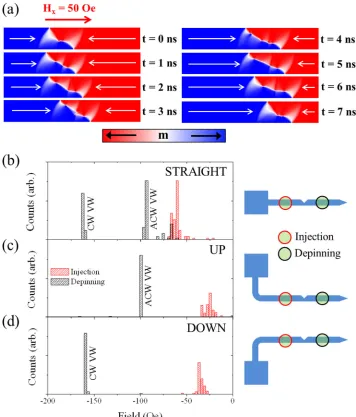
Fig.4(a)presents a simulation of an ACW VDW prop-agating under Hx¼50 Oe, performed using a 2:5 nm
2:5 nm10 nm mesh. The dynamics consisted of periodic
elongations and contractions of the DW, with multiple vor-tices and anti-vorvor-tices forming along its central boundary during the elongation phase. Critically, the basic symmetry of the DW was maintained at all times so that its chirality was always conserved on contracting back to VDW struc-ture. Furthermore, the energy of a bi-domain state contain-ing a TDW was 26% higher than one containcontain-ing a VDW making the pinning of TDWs at defect sites highly unlikely. Therefore, it was expected that by combining this nanowire geometry with the rectifying effects of the corner we could suppress stochastic DW pinning.
To demonstrate this, we fabricated nanowires with the geometries labeled “STRAIGHT,” “UP,” and “DOWN” in Figs.4(b)–4(d). Each nanowire contained a 60 nm deep tri-angular notch where the stochasticity of DW pinning could be probed. Based on our previous results, we expected that T2T VDWs in the “UP” devices would rectify to ACW chir-ality at the r¼1lm corners, while those in the “DOWN” ge-ometry would rectify to CW chirality. We characterized the nanowires’ switching using a focused magneto-optic Kerr effect magnetometer. DW injection and depinning field dis-tributions were measured by performing 100 single shot measurements at the locations indicated in Fig.4.
[image:4.612.49.405.348.765.2]Fig. 4(b) shows data obtained from a “STRAIGHT” nanowire, where a mixture of CW and ACW DWs were expected to pin at the notch. The depinning field distribution showed a high degree of stochasticity with two clear peaks separated by 170 Oe. Based on the results of micromag-netic simulations of VDW depinning fields, we assigned the peak at the lower field to ACW VDWs and the peak at the higher field to CW VDWs. Figs. 4(c) and 4(d) present the results of equivalent measurements on the “UP” and “DOWN” nanowires. Both nanowires exhibited depinning field distributions with a single peak, corresponding to the expected ACW VDWs for the “UP” geometry and CW VDWs for the “DOWN” geometry. We also performed simi-lar measurements on two further devices of each geometry. Across three “STRAIGHT” nanowires, we observed a rela-tively even split between depinning events assigned to ACW and CW VDWs (45% ACW to 55% CW). For the “UP” nanowires, we observed a strong bias towards ACW VDWs (84% ACW to 16% CW), while for the “DOWN” nanowires, we observed the opposite trend (94% CW to 6% ACW). Cumulatively, these results indicate the feasibility of using nanowire corners to suppress stochastic pinning behavior.
In summary, we have shown that the chiralities of VDWs in magnetic nanowires are rectified when they are propagated ballistically into sharp nanowire corners, with the sense of rectification being determined by whether the nano-wires turn left or right. In contrast to previously demon-strated methods of controlling the chirality of propagating DWs,13–15this approach can be implemented in continuous, defect-free, nanowires. Rectification can be suppressed by increasing the radii of nanowire corners, propagating VDWs at low fields, or by increasing the damping constant of the material from which the nanowires are patterned. We have also demonstrated how our approach can be combined with modes of DW propagation that conserve vortex chirality to dramatically reduce the stochasticity of DW pinning at artifi-cial defect sites.
In addition to providing a tool to control VDW chirality in experimental studies this will be useful in chirality-based logic devices11 where the chiralities of VDWs must be switched as they propagate through complex nanowire net-works. Furthermore, corners could be used to “reset” DW chirality to suppress stochastic pinning effects in more con-ventional devices where data is encoded using the orientation of magnetic domains.
This work was supported by the EPSRC (Grant No. EP/ J002275/1). The operation of the microscope was supported
by the Director, Office of Science, Office of Basic Energy Sciences, Materials Sciences and Engineering Division, of the U.S. Department of Energy under Contract No. DE-AC02-05-CH11231. P.F. and M.-Y.I. acknowledge support by the Leading Foreign Research Institute Recruitment Program (Grant No. 2012K1A4A3053565) through the National Research Foundation of Korea (NRF) funded by the Ministry of Education, Science and Technology (MEST).
1G. Hrkac, J. Dean, and D. A. Allwood,Philos. Trans. R. Soc., A369, 3214
(2011). 2
S. S. P. Parkin, M. Hayashi, and L. Thomas,Science320, 190 (2008). 3D. A. Allwood, G. Xiong, C. C. Faulkner, D. Atkinson, D. Petit, and R. P.
Cowburn,Science309, 1688 (2005). 4
R. D. McMichael and M. J. Donahue,IEEE Trans. Magn.33, 4167 (1997). 5
N. L. Schryer and L. R. Walker,J. Appl. Phys.45, 5406 (1974).
6J.-Y. Lee, K.-S. Lee, S. Choi, K. Y. Guslienko, and S.-R. Kim,Phys. Rev.
B76, 184408 (2007). 7
S.-K. Kim, J.-Y. Lee, Y.-S. Choi, K. Y. Guslienko, and K.-S. Lee,Appl. Phys. Lett.93, 052503 (2008).
8M. Hayashi, L. Thomas, C. Rettner, R. Moriya, X. Jiang, and S. S. P.
Parkin,Phys. Rev. Lett.97, 207205 (2006). 9
L. K. Bogart, D. Atkinson, K. O’Shea, D. McGrouther, and S. McVitie, Phys. Rev. B79, 054414 (2009).
10
A. Pushp, T. Phung, C. Rettner, B. P. Hughes, S.-H. Yang, L. Thomas, and S. S. P. Parkin,Nat. Phys.9, 505 (2013).
11K. A. Omari and T. J. Hayward,Phys. Rev. Appl.2, 044001 (2014). 12D. McGrouther, S. McVitie, J. N. Chapman, and A. Gentils,Appl. Phys.
Lett.91, 022506 (2007). 13
E. R. Lewis, D. Petit, L. O’Brien, A. Fernandez-Pacheco, J. Sampaio, A. V. Jausovec, H. T. Zeng, D. E. Read, and R. P. Cowburn,Nat. Mater.9, 980 (2010).
14
J. Brand~ao, R. L. Novak, H. Lozano, P. R. Soledade, A. Mello, F. Garcia, and L. C. Sampaio,J. Appl. Phys.116, 193902 (2014).
15E.-S. Wilhelm, D. McGrouther, L. Heyne, A. Bisig, and M. Kl€aui,Appl. Phys. Lett.95, 252501 (2009).
16
A. Bisig, M.-A. Mawass, M. St€ark, C. Moutafis, J. Rhensius, J. Heidler, S. Gliga, M. Weigand, T. Tyliszczak, B. Van Waeyenberge, H. Stoll, G. Sch€utz, and M. Kl€aui,Appl. Phys. Lett.106, 122401 (2015).
17
The 28 imaging cycles break down as follows: DOWN nanowires-8 imag-ing cycles, input (3 CW, 3 ACW, 2 indeterminate), output (0 CW, 8 ACW). UP nanowires-20 imaging cycles, input (10 CW, 6 ACW, 4 inde-terminate), output (20 CW, 0 ACW).
18OOMMF User’s Guide, Version 1.0, Interagency Report NISTIR 6376,
edited by M. J. Donahue and D. G. Porter (National Institute of Standards and Technology, Gaithersburg, MD, 1999).
19A. Vansteenkiste, J. Leliaert, M. Dvornik, F. Garcia-Sanchez, and B. Van
Waeyenberge,AIP Adv.4, 107133 (2014). 20
G. Woltersdorf, M. Kiessling, G. Meyer, J. U. Thiele, and C. H. Back, Phys. Rev. Lett.102, 257602 (2009).
21W. Bailey, P. Kabos, F. Mancoff, and S. Russek,IEEE Trans. Magn.
37, 1749 (2001).
22
T. A. Moore, P. Mohrke, L. Heyne, A. Kaldun, M. Kl€aui, D. Backes, J. Rhensius, L. J. Heyderman, J. U. Thiele, G. Woltersdorf, A. F. Rodriguez, F. Nolting, T. O. Mentes, M. A. Nino, A. Locatelli, A. Potenza, H. Marchetto, S. Cavill, and S. S. Dhesi,Phys. Rev. B82, 094445 (2010). 23M.-Y. Im, L. Bocklage, P. Fischer, and G. Meier,Phys. Rev. Lett.102,