Terahertz plasmons in coupled two-dimensional semiconductor resonators
O. Sydoruk,1,*J. B. Wu,2A. Mayorov,2C. D. Wood,2D. K. Mistry,2and J. E. Cunningham2
1Optical and Semiconductor Devices Group, Department of Electrical and Electronic Engineering, Imperial College London,
South Kensington Campus, London SW7 2AZ, United Kingdom
2School of Electronic and Electrical Engineering, University of Leeds, Woodhouse Lane, Leeds LS2 9JT, United Kingdom
(Received 8 July 2015; revised manuscript received 24 September 2015; published 9 November 2015) Advances in theory are needed to match recent progress in measurements of coupled semiconductor resonators supporting terahertz plasmons. Here, we present a field-based model of plasmonic resonators that comprise gated and ungated two-dimensional electron systems. The model is compared to experimental measurements of a representative system, in which the interaction between the gated and ungated modes leads to a rich spectrum of hybridized resonances. A theoretical framework is thus established for the analysis and design of gated low-dimensional systems used as plasmonic resonators, underlining their potential application in the manipulation of terahertz frequency range signals.
DOI:10.1103/PhysRevB.92.195304 PACS number(s): 73.20.Mf,73.63.Hs
I. INTRODUCTION
The traditional test beds of terahertz plasmonics are two-dimensional electron systems (2DESs). Early experiments studied plasmon excitation [1,2], thermal emission [3], effects of magnetic fields [2], and dc currents [4]. On the other hand, advances in fabrication and measurement constantly enable discovery of new effects [5]. Theoretical work has traditionally concentrated on the dispersion of gated and ungated plasmons [2,6], magnetoplasmons [2], and edge plasmons [7] in unbounded 2DESs. Analytical studies of plasmonic resonators, however, have been limited mainly to the description of single resonators, either with simple boundaries (in which the resonances occur at multiple half-wavelengths [5]), or with manipulated boundary conditions leading to plasmon instabilities [8]. More complex resonators (realized, for example, by a long periodic grating coupler) have mainly been studied by numerical simulations [9–11].
Several recent experiments, however, have been devoted to systems containing a relatively small number of strongly cou-pled plasmonic resonators. Using an antenna to couple an inci-dent electromagnetic wave, Dyeret al.[12,13] studied the col-lective response of plasmonic crystals comprising up to eleven resonators, with a detector integrated into the crystals. Wu
et al.[14] characterized a system of three coupled resonators by time-domain spectroscopy. They used on-chip LT-GaAs photo-conductive switches monolithically integrated with the 2DESs. The latter experiments are the first to promise a terahertz spec-troscopic characterization where signals transit between the ends of a 2DES (as opposed to the traditional excitation of the whole structure by a grating coupler). The theoretical modeling of the measured spectra then requires new approaches that take into account the coupling between resonators.
A general theoretical method to describe plasmonic struc-tures has been developed by Popov and co-workers. An
Published by the American Physical Society under the terms of the Creative Commons Attribution 3.0 License. Further distribution of this work must maintain attribution to the author(s) and the published article’s title, journal citation, and DOI.
electromagnetic wave is assumed to be incident upon a structure, and the fields are presented in the form of Fourier integrals (for finite structures) [15–18] or series (for in-finitely long periodic plasmonic crystals) [19]. Application of the electromagnetic boundary conditions leads to integral equations for the amplitudes of the harmonics, which can then be found numerically. The structures analyzed include a partially gated infinitely long 2DES [15], a fully gated 2DES with ohmic contacts [16], and a partially gated 2DES with ohmic contacts [17]. The resulting terahertz spectra depend on the spectrum of the plasmonic modes as well as the coupling between a plasmonic mode and the incident electromagnetic wave, and the method is particularly suited to model experiments with a free-space excitation.
The model of Aizin and Dyer [20] presents gated and ungated 2DESs as sections of transmission lines with different impedances. Each section is characterized by a transmission matrix, the product of which can describe the response of a compound resonator. Developed initially for passive struc-tures, the model has recently been extended to terahertz gen-eration in 2DESs carrying a dc current [21]. While the method of Popovet al.takes into account the full fields everywhere in space, much of the attractive simplification of the transmission line model of Aizin and Dyer comes from considering only plasmonic signals at the 2DESs and disregarding retardation. The transmission line could be expected therefore to be particularly suitable for strongly subwavelength plasmons.
An alternative approach to junctions between gated and un-gated 2DESs uses expansions of the electromagnetic fields into eigenmodes [22], which are rigorous solutions of Maxwells equations across the whole junction. It has been conceived for closed metallic waveguides [23–25] and then expanded to include open dielectric waveguides as well [26–28]. It has also been applied to waveguides at optical frequencies [29–33], where metals exhibit a plasmonic response, and to plasmonic waveguides in the terahertz range [34–38]. The technique can be used to characterize a single junction between two waveguides and then analyze more complex geometries (com-prising multiple junctions) relying, for example, on wave [25] or transfer matrices [39].
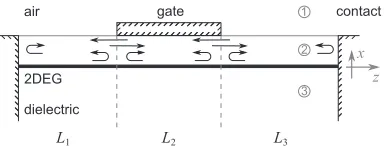
FIG. 1. Two ungated and one gated 2DESs terminated by ohmic constants constitute a system of three coupled resonators, with the contacts and the junctions between the gated and ungated 2DESs acting as plasmonic reflectors.
of systems comprising coupled plasmonic resonators (Sec.II) and compare it directly to the experiments of Wuet al.[14] (Sec.III).
II. THEORETICAL MODEL
The configuration, shown in Fig.1, contains all the basic components of the experimental plasmonic systems: gated and ungated resonators of different lengths and ohmic contacts terminating the system at both ends. The theoretical model includes three steps. First, we find the eigenmode spectra of the gated and ungated 2DESs. We then use these to calculate the plasmon reflection and transmission coefficients at a junction between two 2DESs. From the coefficients, we can derive the resonator modes and simulate the experimentally measured signals.
To calculate the eigenmode spectrum, we assume TM waves with the magnetic fieldHy and the electric fieldsEx andEz.
The angular frequency isωand the longitudinal wave number iskz. The 2DESs are embedded in a homogeneous dielectric
with the permittivityεd.
The electromagnetic waves induce a time-varying modula-tion of the electron densitynand the velocityv. We describe the electron dynamics in 2DESs by the equation of motion of the form
∂v ∂t +
v
τ =
e
mEz|x=0, (1)
where τ is the collision time,e is the electron charge, and m is the effective electron mass. The time-varying current density is J =en0v, where n0 is the dc electron density. Maxwell’s boundary conditions then couple the current and electron density to the fieldsHyandEx.
To find the eigenmode spectra, one has to prescribe the fields is the regions below the 2DES (x <0), between the 2DES and the gate or between the 2DES and the air (0< x < d), and in the air for the ungated 2DES (x > d), whered is the thickness of the dielectric above the 2DES. Denoting these regions correspondingly by 3, 2, and 1, we write the magnetic fields of an eigenmode in the formhyq =Aqexp(ikxa,dx)+ Bqexp(−ikxa,dx). Here,q =1,2,3;Aq andBq are constants;
and the transverse wave numbers in the dielectrickxdand air kxa can be found from the standard dispersion relations for waves in homogeneous dielectrics. We omit everywhere the common factor exp[i(kzz−ωt)].
Because the field amplitudes cannot grow at infinity, the permissible values of the transverse wave numberskxa,d are either purely imaginary or real. When they are imaginary,
FIG. 2. Gated (dashed and dash-dotted) and ungated (solid and dotted) plasmon dispersion curves. The gated dispersion curves were calculated for two different electron densities. The solid line is calculated from the ungated dispersion equation (2) that takes into account the different permittivities of GaAs and air. The dotted line is calculated from a dispersion equation assuming homogeneous GaAs around the 2DES. The plasmon wave numbers for ungated and gated plasmons differ from each other, which contributes to plasmon reflection and transmission at junctions between gated and ungated 2DESs.
the fields decay away from the channel. These wave numbers correspond to plasmons. In the ungated 2DES, they obey a dispersion relation of the form
(1−u)(1+ζ)eikxdd−u(1−ζ)e−ikxdd =0, (2)
whereu=ien0ukxd/(2mε0εdω(ω+i/τ)) withn0u denoting the dc electron density in the ungated 2DES, and ζ = kxd/(kxaεd). In the gated 2DES, the plasmons obey a dispersion relation of the form
ge−ikxdd+(1−g)eikxdd =0, (3)
whereg=ien0gkxd/(2mε0εdω(ω+i/τ)) withn0g denoting the dc electron density in the gated 2DES. Figure 2 shows examples of plasmon dispersion curves. The parameters correspond to the experiments discussed below; the material is GaAs withεd=12.4 andm=0.067m0(m0is the free electron mass). Electron collisions are neglected. The ungated electron concentration isn0u =6.5×1011cm−2(solid line). The gated plasmon dispersions are shown for n0g=6.5×1011 cm−2 (dashed line) andn0g =4.9×1011cm−2 (dash-dotted line). The ungated dispersion curve has a parabolic form; the gated ones are linear at low frequencies (indicating fully gated 2DESs). The thickness of the dielectric above the ungated 2DES and the contrast between the permittivities of air and GaAs affect the ungated dispersion curve. The dotted line in Fig.2shows the ungated dispersion curve assuming a semi-infinite homogenous GaAs layer above the 2DES. The difference between the exact (solid) and approximate (dotted) curves is significant, with the approximate curve giving lower values of frequency for the same wave number.
[image:2.608.313.559.72.179.2]numbers can have any value between zero and infinity. These modes form a continuous spectrum, and the corresponding longitudinal wave numbers are, neglecting losses, either real (radiation modes) or imaginary (evanescent modes).
Any two modes from the same 2DES are orthogonal to each other and obey the orthogonality condition
q
1 εq
hyq(kx)hyq( ˜kx)dx=I(kx,k˜x)δ(kx−k˜x). (4)
The indexq denotes the geometrical region (see Fig.1); the summation goes from 1 to 3 for the ungated and from 1 to 2 for the gated 2DES; the integration limits are determined by the region boundaries;εq equals either 1 orεd;I(kx,k˜x) is a
constant;δ(kx) is the Kronecker delta.
Next, we consider junctions between gated and ungated 2DESs. When a plasmon is incident upon a junction, it will both partially transmit through and partially reflect back from the junction. To find the plasmon transmission and reflection coefficients, we expand the fields at both sides of a junction into the eigenmodes of the gated and ungated 2DESs [22]. One of the expansions contains the incident and reflected plasmon together with the reflected continuous modes; the other contains the transmitted plasmons and the transmitted continuous modes. Maxwell’s boundary conditions require that the transverse fieldsExandHymatch
at the junction. Because of the continuous spectrum of the nonplasmonic modes, the boundary conditions result in two integral equations. Several methods of solving such equations exist, and we adopt here the one based on limiting the size of the regions 1 and 3. We assume that two perfect magnetic conductors are placed in regions 1 and 3 at the same distancew from the 2DES. Since the plasmonic fields decay away from the channel, sufficiently large values ofw do not affect the plasmon dispersions. On the other hand, the presence of the two conductors leads to discrete spectra of the nonplasmonic modes. An advantage of this discretization method is that the effects of radiation can be controlled by the conductor placement. Applying the boundary conditions in each region separately leads for the reflection and transmission coefficients to two algebraic equations of the general form
hyup+Ruhyup+
j
rjhyju
=Tuhygp+
j
tjhyg,
kzuphyup−Rukzuphyup−
j
kzjurjhyju
=Tukzgphygp+
j
kzjgtjhyg, (5)
where the summations are over the nonplasmonic modes, and the incidence is from the ungated 2DES. Truncating the summations at a sufficiently large number and using the orthogonality conditions (4) leads to an algebraic matrix equation for the coefficientsRu,Tu,tj andrj. Alternatively,
Eq. (5) can be solved by the variational method [25], and we found that both approaches gave the same result.
Once the plasmon transmission and reflection coefficients are known for incidence from the ungated (TuandRu) and the gated (TgandRg) 2DESs, the junction between them can be characterized by a wave matrix [25] of the form
1 Tg
TuTg−RuRg Rg
−Ru 1
. (6)
A section of a 2DES of the lengthL, on the other hand, is characterized by a 2×2 diagonal matrix with the diagonal elements exp(±ikzup,gpL).
Finally, we describe compound plasmonic resonators by multiplying the wave matrices. The structure shown in Fig.1 consists of three coupled resonators. To simulate the experiments, we assume that the (perfectly conducting) ohmic contacts, terminating the structure on both ends, leak some signal, in a frequency-independent manner, into and out of the 2DES.
Moderate electron collisions do not affect the mode shapes and, hence, the transmission and reflection coefficients. They do, however, lead to a propagation loss, which can be taken into account by complex-valued plasmon wave numbers kzup,gp. The resonances of the whole structure can be determined from the frequency variation of the wave matrices.
The modal analysis presented here shares several strengths with the theoretical approach of Popov et al. [15–17,19], based on a Fourier representation of the fields. They both are rigorous solutions of Maxwell’s equations, consider the fields everywhere in space, and take effects of retardation into account. However, the modal analysis is able to characterize single junctions, so that complex geometries and be easily analyzed and designed. The price is some loss of generality. We assume, for example, that the ungated resonators of Fig. 1 couple only via the plasmons propagating in the gated resonator (justified for wide gates). On the other hand, the modal analysis may offer advantages compared with the transmission-line approach of Aizin and Dyer [20], in particular when the plasmons are confined loosely to the 2DESs and retardation is important. Finally, by relying in part on analytical calculations, all three approaches would need less computational resources than full-wave numerical simulations. In addition, commercial numerical solvers have currently a limited ability to self-consistently solve problems involving complex electron dynamics (for example, effects of diffusion and dc currents). Analysis of such problems by purpose-built solvers has so far been limited to rather simple geometries [40].
III. COMPARISON WITH EXPERIMENTS
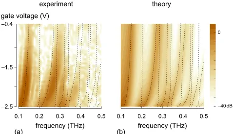
FIG. 3. (Color online) (a) Experimental and (b) theoretical gate-modulated signals (color plots) agree, within the noise floor of the experiments. The signals are determined by the resonances of the whole structure (black lines).
relationship between the applied voltageVg and the electron density asn0g=a1(Vg+a2)γ, wherea1 =5.38×1011 cm−2, a2=2.6,γ =0.23, andVgis in volts.
In our experiments, two LT-GaAs photoconductive switches were connected to the 2DES by ohmic contacts attached to coplanar transmission lines on either side. Terahertz signals generated in one switch traveled through the first coplanar line, the 2DES, and the second coplanar line, before exciting a photocurrent in the far switch. This arrangement enabled on-chip time-domain transmission spectroscopy of the compound plasmonic resonator formed from the 2DESs between 0.05 and 0.5 THz. The structure was kept at a temperature of∼2 K. To increase the signal-to-noise ratio, a gate-modulation technique was used, whereby a small (25 mV rms) gate modulation was superimposed on the static gate voltage, allowing lock-in detection [14]. The measured signal was proportional to the derivative of the photo-excited current with the gate voltage. The (static) gate voltage was varied between−2.5 V (close to pinch-off) and−0.4 V (above which the gate-modulated signals became weak). The measured time variations of the signals were first filtered to eliminate high frequency noise, and then Fourier-transformed to reveal the frequency spectrum of the transmitted pulses.
Figures 3(a) and 3(b) show contour plots of, respec-tively, the experimental and the simulated signals against the frequency and the gate voltage. Both have three distinct features: a strong and narrow feature starting at 0.1 THz for
−2.5 V, with another starting at 0.2 THz, and a weaker broad one around 0.3 THz. Both the theoretically predicted and the experimentally determined signals are stronger at lower frequencies and at larger gate voltages. Overall, they agree best around−2.5 V for all frequencies. The agreement is excellent between the positions of the lowest-frequency feature for the whole voltage range. The experimental and theoretical features that start at 0.2 THz differ somewhat at lower gate voltages. Nevertheless, their shapes are similar; we note in particular that both the theory and the experiments show a frequency broadening between−2.5 and−2 V. The shapes of the third feature around 0.3 THz also agree: both the theory and the experiments start as a broad resonance at−2.5 V and fork into two branches as the gate voltage decreases.
In the simulations, we calculated the derivative of the trans-mitted power with the gated electron density. The plasmons were lossy, first due to collisions (τ =5 ps) and second, due to plasmon leakage into radiation modes at the junctions. Both mechanisms affect the shape of the curves. To simulate the incident terahertz pulse, we assumed that its power decays exponentially with the frequency [14].
Even though a common assumption [5,12,13,36,38], the perfectly reflecting contacts in the simulations is an approxi-mation, since strictly they would not allow coupling between the transmission lines and the 2DESs. The coupling also depends on the fields on both sides of the contact, and it is absent for one of the two modes supported by the transmission line [14]. However, due to the high doping of the contacts and the mismatch of the modal fields, the coupling between the transmission line and the 2DESs is expected to be weak across the whole frequency range. Correspondingly, the real contacts should be good reflectors, and should not strongly shift the phase of the reflected plasmons, or degrade the quality of the resonances considerably. The gate-modulation technique provides acceptable signal-to-noise ratio despite weak plasmon excitation by the transmission lines.
To elucidate further the origin of the measured and simulated signals, Figs. 3(a) and 3(b) also show (dashed black lines) the positions of the resonances calculated for the whole structure. The measured and simulated signals (the contour plots) correspond to some of the calculated resonances. However, not all resonances affect the signals equally. For example, only two of the three lowest resonances (dashed lines) excite a strong signal. Similarly, while three resonances exist around 0.3 THz, only two of them appear to be responsible for two branches originating from the broad third feature in Figs.3(a)and3(b). The reason is that both the experimental and simulated signals are effectively derivatives with respect to the gate voltage and the gated electron density. Consequently, the signals were weak when the derivatives were small (for example, for the resonances of the ungated 2DESs). We calculated the resonant curves ignoring collisions and radiation losses (by takingτ = ∞and by putting magnetic conductors close to the 2DESs).
Although the gate-modulated signals are inherently weak for some resonances, they characterize plasmons directly, unaffected, for example, by a direct cross-talk between the transmission lines on either sides of the 2DESs. The gate-modulation technique is, however, sensitive to frequency variations of the input signals and the coupling strength between the transmission lines and the 2DESs. We were able to take the former effect into account, while assuming that the latter effect is weak. The good qualitative agreement between the experiments and simulations of Fig.3appears to justify this assumption.
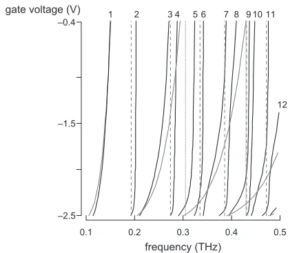
[image:4.608.54.293.74.212.2]FIG. 4. Resonances of the whole system (black lines) and of the uncoupled gated (solid gray) and the two ungated (dashed and dotted gray lines). Interaction between modes co-existing in the same frequency leads to hybridized resonances (e.g., 3 and 4).
The lowest coupled resonance (black line 1 in Fig.4) hardly differs from the lowest uncoupled resonance of the gated 2DES. The next coupled resonance (line 2) is also close to the lowest uncoupled resonance of the longer ungated 2DES. However, the second-order uncoupled resonances of the gated and longer ungated 2DES exist in the same frequency range between 0.2 and 0.3 THz. In the coupled system, they become hybridized (lines 3 and 4). Line 3 starts at −2.5 V as a resonance of the gated 2DES and finishes at−0.4 V as the ungated one; line 4 behaves in the opposite way. Around
−1.5 V, the resonances are coupled, with strong plasmon
amplitudes excited in both 2DESs. A change in the gate voltage will therefore affect not only the plasmons below the gate but also the plasmons in the ungated 2DESs, an effect previously reported in Ref. [17].
The resonances become more entangled as the frequency increases. For example, the next three resonances (lines 5, 6, and 7) stem, at higher gate voltages, from the interaction between three uncoupled resonances (the third-order gated, the third-order longer ungated and the first-order shorter ungated). The interaction creates the broad measured and simulated signals seen in Fig.3around 0.3 THz.
Our model could be used to design further configurations that support hybridized resonances generating strong gate-modulated signals. A candidate structure could comprise two gated 2DESs separated by an ungated 2DES, where uncoupled gated plasmons exist in the same frequency range.
IV. CONCLUSIONS
We have presented an electromagnetics-based approach to characterize coupled plasmonic resonators and compared its predictions with experiments. An analysis of the coupled system showed that while some of the resonances may be independent from each other, most of them hybridize as a result of an interaction between gated and ungated 2DESs. We note that our theoretical approach could be extended for the design of more advanced plasmonic devices, in particular resonant oscillators, amplifiers, and detectors carrying dc currents.
ACKNOWLEDGMENTS
The authors from the University of Leeds thank the EPSRC (grant EP/H007881/1) and ERC (grant TOSCA) for funding.
[1] S. J. Allen, D. C. Tsui, and R. A. Logan,Phys. Rev. Lett.38,
980(1977).
[2] T. N. Theis,Surf. Sci.98,515(1980).
[3] N. Okisu, Y. Sambe, and T. Kobayashi,Appl. Phys. Lett.48,
776(1986).
[4] S. J. Allen, Jr., F. Derosa, R. Bhat, G. Dolan, and C. W. Tu,
Physica B+C134,332(1985).
[5] V. M. Muravev, P. A. Gusikhin, I. V. Andreev, and I. V. Kukushkin,Phys. Rev. Lett.114,106805(2015).
[6] A. L. Fetter,Ann. Phys.81,367(1973).
[7] J. J. Quinn,Solid State Commun.84,139(1992).
[8] M. Dyakonov and M. Shur,Phys. Rev. Lett.71,2465(1993). [9] T. Otsuji, M. Hanabe, T. Nishimura, and E. Sano,Opt. Express
14,4815(2006).
[10] A. R. Davoyan, V. V. Popov, and S. A. Nikitov,Phys. Rev. Lett.
108,127401(2012).
[11] V. Giliberti, A. Di Gaspare, E. Giovine, M. Ortolani, L. Sorba, G. Biasiol, V. V. Popov, D. V. Fateev, and F. Evangelisti,Phys. Rev. B91,165313(2015).
[12] G. C. Dyer, G. R. Aizin, S. Preu, N. Q. Vinh, S. J. Allen, J. L. Reno, and E. A. Shaner,Phys. Rev. Lett.109,126803(2012). [13] G. C. Dyer, G. R. Aizin, S. J. Allen, A. D. Grine, D. Bethke,
J. L. Reno, and E. A. Shaner,Nat. Photon.7,925(2013).
[14] J. B. Wu, A. S. Mayorov, C. D. Wood, D. Mistry, L. H. Li, W. Muchenje, M. C. Rosamond, L. Chen, E. H. Linfield, A. G. Davies, and J. E. Cunningham,Sci. Rep.5,15420(2015). [15] V. V. Popov, O. V. Polischuk, and M. S. Shur,J. Appl. Phys.98,
033510(2005).
[16] V. V. Popov, O. V. Polischuk, W. Knap, and A. El Fatimy,Appl. Phys. Lett.93,263503(2008).
[17] V. V. Popov, A. N. Koudymov, M. Shur, and O. V. Polischuk,
J. Appl. Phys.104,024508(2008).
[18] V. V. Popov and O. V. Polischuk,Tech. Phys. Lett. 36, 272
(2010).
[19] V. V. Popov, G. M. Tsymbalov, and M. S. Shur, J. Phys.: Condens. Matter20,384208(2008).
[20] G. R. Aizin and G. C. Dyer, Phys. Rev. B 86, 235316
(2012).
[21] G. R. Aizin, J. Mikalopas, and M. Shur,arXiv:1506.03491. [22] O. Sydoruk, K. Choonee, and G. Dyer,IEEE Trans. Terahertz
Sci. Technol.5,486(2015).
[23] A. Wexler,IEEE Trans. Microw. Theory Tech.15,508(1967). [24] R. Mitra and S. W. Lee,Analytical Techniques in the Theory of
Guided Waves(Macmillan, New York, 1971).
[26] V. V. Shevchenko,Continuous Transitions in Open Waveguides (Golem, Boulder, Colorado, 1971).
[27] D. Marcuse,Light Transmission Optics(Van Nostrand Reinhold, New York, 1982).
[28] T. Rozzi and M. Mongiardo,Open Electromagnetic Waveguides (IET, London, 1996).
[29] G. I. Stegeman, A. A. Maradudin, and T. S. Rahman,Phys. Rev. B23,2576(1981).
[30] A. A. Maradudin, R. F. Wallis, and G. I. Stegeman,Prog. Surf. Sci.33,171(1990).
[31] R. F. Oulton, D. F. P. Pile, Y. Liu, and X. Zhang,Phys. Rev. B
76,035408(2007).
[32] S. E. Kocabas, G. Veronis, D. A. B. Miller, and S. Fan,Phys. Rev. B79,035120(2009).
[33] S. Thongrattanasiri, J. Elser, and V. A. Podolskiy,J. Opt. Soc. Am. B26,B102(2009).
[34] O. Sydoruk, R. R. A. Syms, and L. Solymar,Opt. Express20,
19618(2012).
[35] O. Sydoruk, R. R. A. Syms, and L. Solymar,J. Appl. Phys.112,
104512(2012).
[36] O. Sydoruk, J. Phys. D: Appl. Phys. 46, 135103
(2013).
[37] O. Sydoruk,J. Phys. D: Appl. Phys.46,345101(2013). [38] O. Sydoruk,J. Appl. Phys.115,204507(2014).
[39] X. Y. He, Q. J. Wang, and S. F. Yu,J. Appl. Phys.111,073108
(2012).