Attenuation of a Shielded Rectangular
Dielectric Rod Waveguide
Colin G. Wells
, Member, IEEE
, and James A. R. Ball
, Member, IEEE
Abstract—The attenuation coefficient of a rectangular dielectric line enclosed by a rectangular shield is obtained by the use of a rig-orous mode-matching method to calculate the required mode field intensity. The cross section of the waveguide is overlaid by a grid, and numerical integration is used to determine the power flow, dielectric, and conductor losses and respective attenuation coeffi-cients. To obtain experimental verification, a length of waveguide was made into a resonator, and measured and calculated factors were compared. The results for the 11mode show how the influ-ence of the shield decreases with distance. This is relevant to the design of dielectric waveguide structures and in filter applications where dielectric resonators are used.
Index Terms—Attenuation, dielectric waveguides, mode-matching methods, numerical analysis, shielding.
I. INTRODUCTION
R
ECTANGULAR dielectric waveguides are used in inte-grated optics, millimeter-wave inteinte-grated circuits, and as transmission lines. Compared to metal waveguides, at mil-limeter-wave frequencies, they have lower propagation loss (depending on dielectric loss), lower cost and are easier to fabri-cate [4]. They are also significantly smaller [1]. Shielded square cross-sectional dielectric resonators are also used in filter appli-cations, e.g., in multimode cubic dielectric-resonator filters [2].The loss in rectangular dielectric waveguides is mostly due to that in the dielectric. However, if the waveguide is surrounded by a rectangular metallic shield (see Fig. 1), then the total loss of the waveguide will also include loss due to induced currents in the inner surface of the shield walls. In a recent paper [9], a modified version of the mode-matching method devised by Sol-bach and Wolf [7] (modified SolSol-bach and Wolf (MSW) method) was used to find the propagation coefficients and field patterns of the hybrid modes of a shielded rectangular dielectric wave-guide. In this paper, the calculated fields for the commonly used mode will be employed to find the wall and dielectric losses of the waveguide and, hence, its attenuation. The effect of the proximity of the shield on the attenuation will also be evaluated.
II. CALCULATING THEATTENUATIONCOEFFICIENT
USINGMODEMATCHING
The modes supported by a rectangular shielded dielectric rod waveguide were investigated using mode matching in a recent
Manuscript received June 7, 2005; revised January 23, 2006. The work of C. G. Wells was supported by the University of Southern Queensland under a scholarship.
The authors are with the Department of Engineering, University of Southern Queensland, Toowoomba, Qld., Australia.
[image:1.594.305.547.167.258.2]Digital Object Identifier 10.1109/TMTT.2006.877056
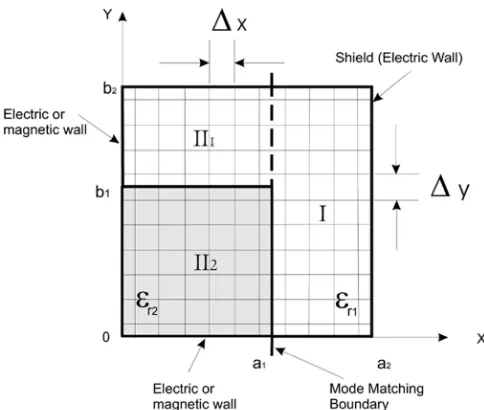
Fig. 1. Shielded dielectric rod waveguide.
Fig. 2. One quadrant of the cross section showing the grid for power loss cal-culation.
paper [9]. The cross section was divided into three separate re-gions, and the field within each region represented as a sum of basis functions particular to the region. Due to symmetry, it was only necessary to consider one quadrant of the cross section for which the mode-matching regions are as shown in Fig. 2. Conti-nuity of the tangential fields was then enforced at the boundaries between the regions, allowing the amplitudes of the basis func-tions to be determined. Once this has been accomplished, the field components of any required mode can be calculated at any point in the cross section.
To calculate the power losses within the waveguide, the cross section is overlaid with a grid with lines spaced at and , as illustrated in Fig. 2. Field values and power densities are cal-culated at each intersection of the grid lines, and the total power flow and power dissipation is found by numerical integration.
[image:1.594.304.546.304.509.2]the total power flow is found by writing (2) as
(3)
where and identify the and nodes in regions and , respectively.
If the dissipation in the walls and dielectric is sufficiently small, the fields within the waveguide will be almost the same as in the lossless case. This allows both types of losses to be es-timated from the lossless fields using the perturbation method [6].
The dielectric power loss per unit length over the cross section can be obtained from
(4)
and
where is the permittivity of free space, is the dielectric loss factor, is the real part of the dielectric relative permittivity in region , and is the dielectric loss tangent.
The numerical form of (4) is
(5)
where the index identifies nodes in region .
The conductor loss per unit length in the shield walls can be obtained from
(6)
(7)
where identifies nodes, on the top shield boundary
spaced apart, and the index identifies points on the right-hand-side shield boundary
with spacing . Also in (3), (5), and (7), each component of or , at a point, is the sum of a number of basis function values calculated using the MSW method.
By substituting the spatial grid component values into these equations, a close approximation to the power flow and losses can be obtained for the structure. Since (3), (5), and (7) are ob-tained from 4 the quarter structure of Fig. 2, duplication of common points at the boundaries must be taken into account.
From [6], the attenuation coefficient due to dielectric loss and shield wall loss can then be calculated using
(8)
where and are the dielectric loss and attenuation and shield wall loss and attenuation, respectively.
In practice, conductor loss is increased by surface roughness, and this is normally taken into account by multiplying the theo-retical value of the surface resistance by a roughness factor [5].
III. ALTERNATIVEMETHOD OFCALCULATING THE
ATTENUATIONCOEFFICIENTDUE TODIELECTRICLOSS
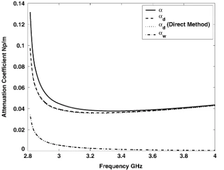
Fig. 3. Attenuation coefficient versus frequency for theE mode. The SDR isSDR = a =a = 2.
The perturbation method using the grid is preferred to the above direct method, as it can be used to find both shield wall loss and dielectric loss. It is also much faster to compute. How-ever, since fields from the lossless solution are used to estimate the dissipation, some additional error is involved. In Section IV, dielectric loss results obtained by both methods are compared to show that the additional error cost of the perturbation approxi-mation is negligible.
IV. DISCUSSION OFCALCULATEDRESULTS
The attenuation coefficients created by the dissipation within the dielectric and shield walls were calculated for the commonly used mode using the grid method described in Section II. The dielectric rod material is barium tetratitanate for which the loss tangent is specified by the manufacturer (picoFarad, Ana-heim, CA) as
Frequency GHz (9)
This material was also used to obtain the experimental results presented later. A surface roughness factor of unity has been as-sumed for the metal shield. The attenuation coefficient verses frequency (beginning near cutoff) with a shield to dielectric di-mension ratio (SDR), , is shown in Fig. 3. The plot of the attenuation coefficient verses SDR with the fre-quency at 3.4 GHz is shown in Fig. 4.
For the mode shown in Fig. 4, as shield size increases relative to the dielectric, is gradually dominated by a rela-tively constant . This indicates that when using a dielectric with a relative permittivity of around 37, choosing an
will minimize the shield conductor loss.
[image:3.594.54.277.67.236.2]The size of grid used in these plots was 51 51 points for one-quarter of the structure. The values marked with “ ” and “*” on the plots are generated from an extrapolation of the con-vergence of the attenuation coefficient with an increase in grid size. The maximum grid used in this convergence process was 501 501. The comparison of these values show that a grid size
Fig. 4. Attenuation coefficient versus SDR for theE mode. The frequency is 3.4 GHz.
of 51 51 (very efficient to compute) should be of sufficient ac-curacy for SDR values down to 1.1. Below this, larger grid sizes will be required.
To estimate the extra error due to the perturbation approx-imation, which is inherent in the grid method, of the mode was also calculated directly using the MSW method, as described in Section III. The results are shown in Figs. 3 and 4, and show excellent agreement with the grid method extrapo-lated values.
As , the mode becomes , and the
coupled modes become the mode. The -and -like qualities of these modes, in a cross section of the dielectric region, can be seen in Figs. 5 and 6, respectively. Hence, a further check of the grid method was performed by analytically calculating the perturbation approximations for and in a square cross-sectional waveguide completely filled with dielectric [6]. These were compared to those obtained from the grid method as the SDR value is brought very close to 1. To obtain the best accuracy, the grid method values, as mentioned before, were obtained from an extrapolation of the convergence of the attenuation coefficient with an increase in grid size. The dimensions of the waveguide used were the same as the dielectric rod used in experimental measurement, i.e., a 12.05-mm square cross section ( ) at a frequency of 3.4 GHz and with calculated for the dielectric at that frequency. The results, shown in Table I, show a difference of less than 2%.
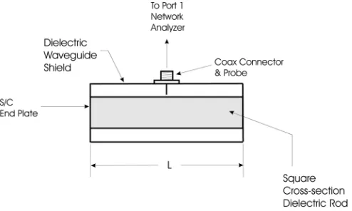
V. MEASUREMENTTECHNIQUE
To verify the grid mode-matching method for finding loss, comparisons of calculated and measured unloaded were made for the mode using two sizes of resonator.
Fig. 6. Electric and magnetic field patterns in thexy-plane for the coupled
E =E modes. For clarity, the electric field intensity in the dielectric isx5. (Color version available online at http://ieeexplore.ieee.org.)
TABLE I
COMPARISON OFEXTRAPOLATEDGRIDMETHODATTENUATIONCOEFFICIENT
RESULTS(Np/m)FOR THESHIELDEDRECTANGULARDIELECTRIC
WAVEGUIDE,ATSDR = 1,ANDTHOSECALCULATED FOR
DIELECTRICFILLEDRECTANGULARWAVEGUIDE
(a = b = 6:025mm," = 37:13, Frequency= 3:4GHz)
provide consistent results, the same dielectric rod was actually used in both resonators. The waveguides cross sections were 23.8 23.8 mm and 18 18 mm, giving SDR values of 1.98 and 1.49, respectively.
The measurements of the unloaded were carried out using a form of the amplitude reflection method [3].
The unloaded of a resonator can be calculated from
(10)
where is the frequency at resonance, is 4 the energy stored in the three regions of Fig. 2 over the resonator length, and
and are the dielectric, wall and end plate losses in the resonator, respectively.
The total energy stored in the resonator over the full cross section can be calculated from
(11)
and the propagation coefficient will be
(12)
where is the number of half-wavelengths of the resonant mode under investigation. Furthermore, the variation of the components of in this type of resonator will be of the form or . After integration with respect to , (11) can be written as
(13)
where is a function of the transverse coordinates only. In Reimann sum form,
(14)
[image:4.594.56.279.66.182.2] [image:4.594.53.278.227.344.2]TABLE II
COMPARISON OFCALCULATED ANDMEASUREDQVALUES FOR THE
153.3 -mm-LONGSQUARECROSS-SECTIONALDIELECTRICROD
RESONATOR ATN HALF-WAVELENGTHS(a = b = 6:025mm,
a = b = 11:9mmAND9 mm)
Alternatively, the energy stored in the cavity may be obtained from the power flow in the infinite waveguide (3)
(15)
where is the group velocity, obtainable numerically. Similarly, the dielectric and wall losses within the cavity can be obtained from the corresponding waveguide losses per unit length as follows:
(16) (17)
The end-plate loss, for both ends and the full cross section of the resonator, can be calculated from
(18)
which becomes in Reimann sum form
(19)
VI. COMPARISON OFCALCULATED ANDMEASUREDRESULTS
The reflection coefficient values for resonances of the mode were measured over a frequency range from cutoff to 4.2 GHz. When comparing the measured factor results to cal-culated values, it is necessary to account for surface roughness. The average surface roughness due to the milling process was estimated as 3.2 m. Given that the shield material is brass con-taining 38% zinc with a conductivity of 1.57 10 m, a sur-face roughness factor of approximately 1.7 is predicted from [5]. The method used in [5] assumes that the surface profile shows
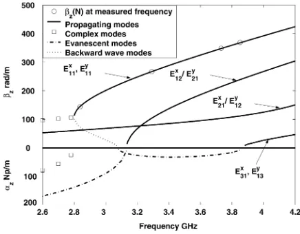
[image:5.594.316.534.302.472.2]Fig. 8. Calculated propagation coefficient values for the first few modes to propagate, with measurements of theE mode superimposed. Shield dimen-sion ratioSDR = 1:49.
Fig. 9. Calculated propagation coefficient values for the first few modes to propagate, with measurements of theE mode superimposed. Shield dimen-sion ratioSDR = 1:98:.
a regular variation, e.g., a sawtooth. The actual surface profile is likely to be more complicated than this. Therefore, a surface roughness factor of 2 was used to calculate the -factor values. A comparison of measured and calculated values is shown in Table II. Percentage differences of the measured values with re-spect to the calculated values are shown in the right-hand-side column. From this, it can be seen that, on average, the measured -factor values are too low by approximately 5%. The most probable reason for this is the flange contact resistance of the short-circuit end plates, which were bolted on, not soldered [8]. Not all possible resonances were able to be measured. It was found that some resonances did not couple well to the probe and, thus, were too noisy. Other resonances were found to be affected by significant coupling to the degenerate mode , which made accurate unloaded calculations impossible at these frequen-cies.
It is believed that these results for the rectangular dielectric rod waveguide have not previously appeared in the literature. The method is confirmed by a close comparison with a direct method for calculating the attenuation coefficient due to the dielectric and also with analytically calculated values for a rectangular waveguide completely filled with dielectric. The method is also validated by good comparison of the measured and calculated values of the shielded dielectric rod wave-guide when used as a resonator.
The results of this paper will be relevant to the design of electric waveguide structures and in filter applications where di-electric resonators are used.
ACKNOWLEDGMENT
The prototype dielectric shielded line was manufactured at the University of Southern Queensland (USQ) Mechanical En-gineering Workshop by C. Galligan.
REFERENCES
[1] A. G. Engel, Jr. and L. P. B. Kathi, “Low loss monolithic transmission lines for submillimeter and terahertz frequency applications,”IEEE Trans. Microw. Theory Tech., vol. 39, no. 11, pp. 1847–1854, Nov. 1991.
[2] I. Hunter, Theory and Design of Microwave Filters, ser. Electromag-netic Wave Series. London, U.K.: IEE Press, 2001.
[3] D. Kajfez and E. J. Hwan, “Q-factor measurement with network an-alyzer,”IEEE Trans. Microw. Theory Tech., vol. MTT-32, no. 7, pp. 666–670, Jul. 1984.
Colin G. Wells(S’02–M’05) was born in Sydney, Australia, on April 3, 1951. He received the B.Eng. degree in electrical and electronic engineering and Ph.D. degree from the University of Southern Queensland, Toowoomba, Qld., Australia, in 2002 and 2006, respectively. His doctoral dissertation concerned the design of microwave components and filters using the mode-matching technique.
James A. R. Ball(M’81) was born in Guildford, U.K., on February 11, 1943. He received the B.Sc. degree in engineering from Leicester University, Leicester, U.K., in 1964, the M.Sc. degree in physics from the University of London, London, U.K., in 1968, and the Ph.D. degree in electrical engineering from the University of Queensland, Queensland, Qld., Australia, in 1988.