JOURNAL OF LIGHTWAVE TECHNOLOGY, VOL. 35, NO. 12, JUNE 15, 2017 2339
Positioning and Space-Division Multiple Access
Enabled by Structured Illumination With
Light-Emitting Diodes
Johannes Herrnsdorf, Member, IEEE, Michael John Strain, Erdan Gu, Robert K. Henderson, and Martin D. Dawson
Abstract—Self-location of devices in an illuminated area can be realized using light-emitting diode array luminaires with in-tegrated electronic smart control. These smart lighting sources project a rapidly displayed time sequence of spatial illumination patterns onto the scene, which enables positioning on a millisec-ond timescale. We demonstrate a prototype system based on a CMOS-driven 16× 16 array of GaN light-emitting diodes and its application to space-division multiple access in a Gb/s optical wireless network.
Index Terms—Light-emitting diodes (LEDs), localization, nav-igation, position measurement, space-division multiple access, wireless optical.
I. INTRODUCTION
W
ITH the advent of light-emitting diode (LED) based solid state lighting, much excitement has centered around so-called “smart lighting”, which is energy saving on the one hand, but on the other, offers advanced functionality. This functionality may include intelligent intensity control, ac-tive color balance, electronic control systems and data trans-mission. These schemes are enabled by the favorable properties of GaN-based LEDs such as low power consumption, compact dimensions, easy integration with control electronics and color converters, availability of LEDs throughout the visible spectrum and fast modulation response.Manuscript received May 16, 2016; revised November 30, 2016; accepted February 19, 2017. Date of publication February 21, 2017; date of current version April 20, 2017. This work was supported by the Engineering and Physical Sciences Research Council under Grant EP/M01326X/1, QuantIC. The underlying data for this work can be found at [1].
J. Herrnsdorf, M. J. Strain, E. Gu, and M. D. Dawson are with the Institute of Photonics, Department of Physics, University of Strathclyde, Glasgow G1 1RD, U.K. (e-mail: [email protected]; [email protected]; [email protected]; [email protected]).
R. K. Henderson is with the Joint Research Institute for Integrated Systems, Institute for Micro and Nano Systems, School of Engineering, University of Edinburgh, Edinburgh EH93JL, U.K. (e-mail: [email protected]).
This paper has supplementary downloadable multimedia material available at http://ieeexplore.ieee.org provided by the authors. The supplementary file contains a video of real-time positioning and space-division multiple access using structured illumination. At first, it is shown how two detectors in the illuminated area receive a positioning signal transmitted at 2000 fps. Once their position is known, individual wireless optical data streams are sent to each detector at 1 Mb/s/channel. This is shown from two different angles. Afterwards, it is shown how the position of a single detector is traced in real-time. This material is 43.8 MB in size.
Color versions of one or more of the figures in this paper are available online at http://ieeexplore.ieee.org.
Digital Object Identifier 10.1109/JLT.2017.2672864
Here, we report a scheme of smart lighting that allows ac-curate determination of the position of devices within the il-luminated area. Stimulated by the development of LED based communications systems [2], LED-based positioning systems are the subject of considerable interest [3]–[6]. Earlier reports used a relatively small number of LED emitters and provide positioning through time difference of arrival ranging [3], [7], [8], allocation to fingerprinted luminaires, often combined with signal strength evaluation [9]–[11], probabilistic methods [4], or a range of different triangulation methods [3], [4], [12], [13]. This work presents a scheme where the position information can be retrieved from a time-sequence of spatial illumination patterns which provide fingerprint optical signals for each spa-tial site. The modulation format of each individual LED element is relaxed in this scheme as compared with other fingerprinting methods, and in particular projection-based approaches such as that reported by Taylor and Hranilovic [10]. Crucially, there is no requirement for orthogonal modulation in the method detailed here. The use of spatial illumination pattern sequences provides uniform illumination across the scene and is implemented using a single-chip transmitter. This scalable approach allows signif-icant simplification at the receiver end, which is beneficial e.g. for applications related to the internet of things [14], whilst at the same time providing high positioning accuracy and speed. As shown schematically in Fig. 1, the LED light source comprises a dense array of microscopic LED elements which project a spatial-temporal pattern sequence onto the scene. The sequence is displayed at a pattern update rate beyond visual flicker recog-nition. Devices with a photodetector within the illumination area monitor the time sequence signal, uniquely defining their posi-tion within the scene. An uplink from the device to the pattern generator is not needed and the geometry of the array can be adapted to the geometry of the room. Based on this system, positioning within a time of less than 10 ms can be achieved using a single photodiode as receiver and computationally un-demanding decoding.
One possible application of this positioning system is the provision of multiple-access in a multi-user Light-Fidelity (Li-Fi) system [15]–[19]. Here we demonstrate how the position information can be used to supply individual data streams to 16 connected devices with an aggregate data rate in excess of 1 Gb/s using on-off keying (OOK). This implementation of space-division multiple access provides a high overall data rate because the individual connected devices are not required to
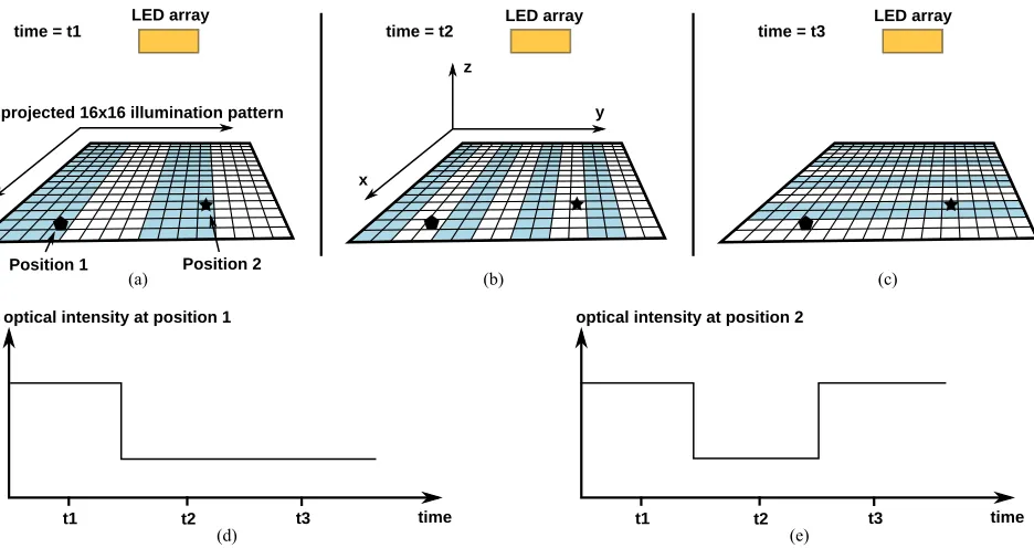
Fig. 1. Schematic of the positioning system. (a)–(c) illustrate three different timest1, t2, t3. At each of these times, a different illumination pattern is projected by the LED array, where the blue and white checkerboard squares correspond to grid sites with binary high or low optical intensity. Two exemplary positions within the projection area are indicated by a pentagon and a star. The time-sequence fingerprints corresponding to these two sites are shown in (d) and (e).
share transmitter bandwidth, and it also enhances security as the individual connections are highly directional and therefore less prone to interception.
The applications of this work are not limited to smart lighting. For example, the same approach can potentially be used in microscopy for automated location of a bright (e.g. fluorescent) object within the field of view.
II. POSITIONINGWITHSTRUCTUREDILLUMINATION
A. Local Fingerprinting With a Projected LED Array
A system has been developed to follow the schematic of Fig. 1. The light source comprises ann×mLED array and optics which project the array output onto the scene. Thus, any device equipped with a photodetector detects the emission of one corresponding pixel (“checkerboard square”) within the array. In the simplest case, positioning can now be achieved by raster-scanning through the array, i.e. one pixel is switched on at a time. Therefore, a device that is synchronized to the transmitter clock can identify from which pixel it receives a signal and thus knows its position.
A more practical implementation employs a sequence of suit-able binaryn×mpatterns rather than raster scanning. For ex-ample, the Hadamard basis, which has been used for image compression and single pixel cameras [20], has the benefit that each pattern has half of the pixels switched on instead of a single pixel. This provides a higher illumination level suitable for lighting. Receiving devices record the intensity they receive from each pattern and can subsequently determine their position using a decoding algorithm. Since the position signal provided by the Hadamard basis is over-determined, we are able to use a subset of the Hadamard basis consisting of k= 2 log2(N)
Fig. 2. The 16×16 micro-LED array with integrated CMOS control that was used for this work: (a) cross-sectional schematic of the integration of LED chip and CMOS chip, (b) plan view micrograph of the device displaying pattern number 9 of the pattern sequence, and (c) the 16 patterns used for positioning.
HERRNSDORF et al.: POSITIONING AND SPACE-DIVISION MULTIPLE ACCESS ENABLED BY STRUCTURED ILLUMINATION WITH LED 2341
in Section II-B. Note that the LED elements do not need to be arranged in a square or rectangular fashion but can be arranged in any suitable geometry.
Since the pattern sequence as well as an embedded clock sig-nal for synchronization can be implemented in the transmission protocol, no uplink from the device to the structured illumination ceiling light is required. The scheme can be supplemented by technologies currently being developed for Li-Fi. For example, a fast modulation on top of the pattern sequence can enhance robustness to ambient light and compatibility with dimming. The knowledge of the device position can be exploited to pro-vide individual data streams to devices in a multi-user Li-Fi environment.
B. Position Encoding in Spatio-Temporal Illumination Pattern Sequences
In our demonstrator system, the 16× 16 spatial locations can be uniquely identified by an 8-bit fingerprint. If we transmit these 8 bits using Manchester encoding, a total of 16 on/off states will be transmitted. The 16 illumination patterns shown in Fig. 2(c) are chosen such that each spatial site is assigned a unique Manchester-encoded 8-bit sequence. The computational complexity in this setup is thus reduced to retrieving these 8 bits from the received optical signal.
Generalisation to arbitrary array sizes is done by first con-sidering ann×marray wherenandmare powers of 2. Then each spatial site can be uniquely identified by a fingerprint of
log2 n+ log2 m bits, which is transmitted in a Manchester-encoded on/off sequence of the corresponding LED element. The assignment of location words to the spatial sites is in prin-cipal arbitrary and in our demonstration was chosen such that stripe-patterns were generated that are at the same time a subset of the n×m Hadamard basis. This way, the spatial patterns are orthogonal to each other, which is a convenient choice if a remote monitoring or tracking functionality based on single-pixel imaging [20] is added to the system. Manchester encoding maintains the same duty cycle for each LED and thus provides an even illumination level across the scene. Other array dimen-sions and non-rectangular configurations can also be addressed by assigning location fingerprints of sufficient length to the spa-tial sites. Synchronization with the transmitter clock is achieved by adding two illumination patterns as a start/stop bit where all LEDs are first turned off and then on.
It is possible to choose fingerprints longer than log2 n+ log2 mbits, for example in order to improve the signal to noise ratio (SNR) and error tolerance [14]. All of these sequences have in common that they encode the position information in a unique on-off sequence seen by the receiver, thus eliminating the computational effort needed by methods based on triangulation, time of arrival, or probabilistic approaches.
III. TRANSMITTER
We use a 16×16 array of 100×100µm2 GaN LED pixels (98% area fill factor) emitting at 450 nm. The LED array was bump-bonded to a custom-designed complementary metal oxide semiconductor (CMOS) driver chip enabling fully individual
control of bright pixels in a compact format [21]–[26]. A schematic and an optical micrograph of the device are shown in Fig. 2. A few defects are visible which can be short circuit (no occurence on the particular device used here), open circuit (4 occurences) or where neighboring pixels can be inadvertantly interconnected (28 pixels affected). The number of defects in this prototype device can be reduced by optimizing the man-ufacturing process. For positioning, it is not required to use such a CMOS-integrated device but it has several advantages such as small footprint, simple projection and digital electronic interface.
The individual pixels in these devices respond with a full on-off modulation bandwidth of up to 110 MHz [24]. The pattern update rate is 2 kfps limited by a serial data link in the current electronic implementation. Future devices may be able to oper-ate at Mfps frame roper-ates. The 16×16 CMOS-controlled array has 16 individual data inputs which modulate the columns of the array. Note that these devices are designed for OOK and are capable of a maximal data rate of about 500 Mb/s for a single pixel [24]. However, when applying more sophisticated encod-ing schemes to LEDs of similar dimensions, data rates of several Gb/s from a single micro-LED have been demonstrated [27].
The logic inputs to the CMOS control chip were supplied through a field-programmable gate array (FPGA) operating at up to 150 MHz and the electrical power was supplied through a universal serial bus (USB) connection. This way, the entire device is driven through a single USB cable, which is a more practical implementation than our earlier work where the logic inputs were directly connected to high-speed bit error rate (BER) test equipment, voltages higher than the 5 V available from USB were applied and only few pixels were operated in parallel [24], [28], [29].
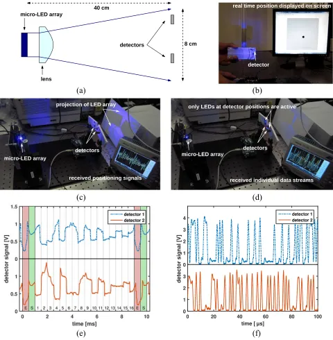
Fig. 3(a)–(d) show the current lab-scale implementation of the system. An aspherical lens with 8 mm focal length and a numerical aperture of 0.5 was used to project the patterns onto a plane at 40 cm distance, providing a scene illuminated area of 8×8 cm2. As indicated Fig. 3(a), photodetectors were placed arbitrarily within the scene. The operation is insensitive to the orientation of the photodiodes as long as the line-of-sight signal is incident within the field-of-view of the bare photodiode chip. Optics could be used to tailor the field of view if desired. Mul-tipath propagation would lead to an increase of the background noise, i.e. reduction of the SNR. Due to the large depth of focus of the projection optics in this setup, positioning was observed to be insensitive to vertical displacements of the photodetectors out of the projection plane.
We have also verified experimentally that positioning can be achieved by the same system if retro-reflective elements are placed in the scene and the back-reflected optical signal is mon-itored by a remote photodetector which is placed next to the transmitter.
IV. DEMONSTRATION OFREAL-TIMEPOSITIONING
Fig. 3. Demonstration of positioning of detectors and subsequent individual data streaming: (a) Schematic of the setup. (b) Video-still from a real-time positioning demonstration at 333 fps. Photographs of (c) positioning at 2 kfps and (d) individual data streams sent to each detector at 1 Mb/s/channel. (e) Individual optical signals recorded in the positioning mode, corresponding to (c). The start bit interval is highlighted in green and marked with “S”, the stop bit interval is highlighted in red and marked with “E”, and the time intervals of the 16 patterns shown in Fig. 2(c) are indicated. The detector positions arex1 =4.5 cm,y1 =5 cm for detector 1 andx2 = 2cm,y2 = 3cm for detector 2. (f) Individual optical signals recorded in the data transmission mode corresponding to (d).
in other Li-Fi implementations AC-coupled detection can be used in order to make the system robust against low-frequency ambient noise. Fig. 3(b)–(d) show photographs of the system during operation and a video showing the system in opera-tion can be found at [1]. The pattern sequence is displayed at a frame rate of up to 2 kfps. Above 1 kfps, no visual flicker was observed. We employ a pattern sequence consisting of 16 patterns plus a start bit (all LEDs on) and a stop bit (all LEDs off). Hence, position information is obtained within 9 ms as shown in Fig. 3(e).
HERRNSDORF et al.: POSITIONING AND SPACE-DIVISION MULTIPLE ACCESS ENABLED BY STRUCTURED ILLUMINATION WITH LED 2343
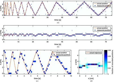
Fig. 4. Trajectory of a photodiode moved back and forth along a circular arc as shown in Fig. 5: (a) recordedx-coordinate and (b) recordedy-coordinate of the photodiode as a function of time. The solid line represents the position according the input signals to the motor. (c) Detail of (a). (d) Trajectory in thex−y-plane. The solid red line shows the arc taken by the detector and the color coding indicates how often a given position was recorded by the positioning system during the experiment.
a frame rate of 333 fps, limited by the sampling capability of the Arduino board with 5-value median filtering. The process-ing capability of the Arduino chip was not limitprocess-ing because the decoding algorithm is computationally cheap. Note that this pro-totype was operated under typical laboratory ambient lighting conditions.
Fig. 4 shows the real-time traced position of a photodiode that was moved back and forth along a circular arc of 43.2◦ and 103 mm radius by a stepper motor with 1.8◦step angle. A schematic of this configuration is shown in Fig. 5. The position data was recorded by the Arduino board with a position update rate of 6.7 Hz, limited by the pattern rate of 333 fps and the over-head needed for the synchronization with the embedded optical clock signal. As can be seen in Fig. 4(c), position information is still obtained at motion speeds where more than one pixel is crossed during the time taken for one position update. A slight lag of about 100 ms is visible which is due to the number of transmitted symbols that need to be received for clock synchro-nization and location estimation. This means that an increase of the pattern rate will reduce this lag. No measures for error de-tection were taken and the position accurracy was 8.2 mm RMS, corresponding to 1.64 pixels. In Fig. 4 several spurious location estimates can be seen. 10% of the position readings deviated
Fig. 5. Schematic of the setup used to demonstrate real-time tracking. The data recorded by this setup is shown in Fig. 4.
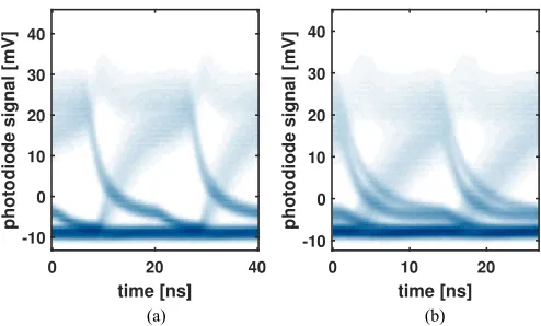
Fig. 6. Representative eye diagrams of one of 16 data channels operated in parallel at (a) 50 Mb/s/channel and (b) 75 Mb/s/channel.
V. APPLICATION TOMULTIPLEACCESS IN AMULTI-USER LI-FIENVIRONMENT
A multi-functional demonstration was designed to illustrate the spatial recognition of two separate detectors and subsequent individual data transmission to these detectors from a single ar-rayed LED source. For individual data transmission, two LEDs corresponding to the locations of the two detectors (and thus imaged to the detector) were switched on. Each of these two LEDs was modulated with an individual data signal at 1 Mb/s, limited by the bandwidth of the detector. This mode of opera-tion is shown in Fig. 3(d) and the video at [1]. Representative received optical signals are shown in Fig. 3(f).
The data transmission rates of the individual data channels were assessed with an AC-coupled fast photodiode with 1.4 GHz bandwidth connected to an oscilloscope with 1 GHz bandwidth. In this case, 16 LEDs of the array were switched on, each carry-ing an individual data signal. The transmitted data streams con-sisted of 16384 bits per channel, which is limited by the memory available on the FPGA. The first 84 bits of these streams were set to a fixed sequence of 83 zeros and 1 one in order to pro-vide a trigger signal for the detector. The remaining 16300 bits were filled with a pseudo-random bit sequence, where the se-quences of the 16 different channels were uncorrelated with each other. Hence, the setup is useful for measuring a BER above 6.14×10⁻⁵.
At 50 Mb/s per channel (800 Mb/s aggregate data rate), not a single bit error occured and at 75 Mb/s/channel (1.2 Gb/s) the BER was 3.5×10⁻⁵. In both cases, the measured BER is below the detection limit of 6.14×10⁻⁵. At 85 Mb/s/channel (1.36 Gb/s) the BER was 8.7×10⁻⁴ and at higher data rates the BER exceeded 10−3. Representative eye diagrams of one channel are shown in Fig. 6. Note that the off-state appears much more clearly defined than the on-state. This is because of the electrical cross-talk through the shared n-contact that affects pixels being switched on at the same time but does not affect pixels that are switched off [26].
By regular switching between positioning and data transmis-sion mode, a single transmitter device can provide reconfig-urable individual connections to moving network nodes in the area.
VI. CONCLUSION ANDOUTLOOK
Lighting by smart arrays of LEDs with integrated CMOS con-trol enables self-positioning of devices in the illuminated area within 10 ms. This is possible by structured illumination with a suitable spatial illumination pattern sequence. In principle, fu-ture implementations should allow positioning within less than 10µs if the control electronics are specifically engineered to harness the MHz bandwidth of the LEDs. The accuracy and area coverage are scalable via the number of emitters and the projection optics used. Here, we demonstrated a precision of 5 mm over a distance of 40 cm, though in principle the projec-tion of the array can be demagnified to microscopic dimensions or extended to cover areas of several meters across. There is scope to achieve a resolution better than the sampling grid by defocussed projection and development of a suitable decoding algorithm using spatial interpolation, though this requires or-thogonal modulation of the LEDs and increases the complexity at the receiver end [10].
The potential applications of this technology are wide-ranging. As an example, we have demonstrated wireless optical space-division multiple access to 16 connected users at an ag-gregate data rate of 1.2 Gb/s with a BER of less than 10−4. The capability of doing so with a single-chip transmitter is an intrin-sic property of the positioning method presented here. Again, improvement by dedicated engineering is possible. The under-lying technology has been shown earlier to provide high optical power [26] which is required for projection over a few meters in this type of application.
REFERENCES
[1] “Data,” 2016. [Online]. Available: http://dx.doi.org/10.15129/813f5f64-b709-4c0f-8dcd-097ad2ef5381
[2] T. Komine and M. Nakagawa, “Fundamental analysis for visible-light communication system using LED lights,” IEEE Trans. Consum.
Elec-tron., vol. 50, no. 1, pp. 100–107, Feb. 2004.
[3] J. Armstrong, Y. A. Sekercioglu, and A. Neild, “Visible light position-ing: A roadmap for international standardization,” IEEE Commun. Mag., vol. 51, no. 12, pp. 68–73, Dec. 2013.
[4] T.-H. Do and M. Yoo, “An in-depth survey of visible light communication based positioning systems,” Sensors, vol. 16, no. 5, 2016, Art. no. 678. [Online]. Available: http://www.mdpi.com/1424-8220/16/5/678 [5] M. Nakajima and S. Haruyama, “New indoor navigation system for
vi-sually impaired people using visible light communication,” EURASIP J.
Wireless Commun. Netw., vol. 2013, no. 1, pp. 1–10, 2013. [Online].
Available: http://dx.doi.org/10.1186/1687-1499-2013-37
[6] M. Biagi, S. Pergoloni, and A. M. Vegni, “LAST: A framework to localize, access, schedule, and transmit in indoor VLC systems,” J. Lightw. Technol., vol. 33, no. 9, pp. 1872–1887, May 2015.
[7] S. Y. Jung, S. Hann, and C. S. Park, “TDOA-based optical wireless indoor localization using led ceiling lamps,” IEEE Trans. Consum. Electron., vol. 57, no. 4, pp. 1592–1597, Nov. 2011.
[8] J. H. Y. Nah, R. Parthiban, and M. H. Jaward, “Visible light communica-tions localization using TDOA-based coherent heterodyne detection,” in
Proc. 2013 IEEE 4th Int. Conf. Photon., Oct. 2013, pp. 247–249.
[9] A. S. Martinez-Sala, F. Losilla, J. C. Snchez-Aarnoutse, and J. Garca-Haro, “Design, implementation and evaluation of an indoor navigation system for visually impaired people,” Sensors, vol. 15, no. 12, pp. 32168–32187, 2015. [Online]. Available: http://www.mdpi.com/1424-8220/15/12/29912 [10] M. T. Taylor and S. Hranilovic, “Angular diversity approach to indoor positioning using visible light,” in Proc. 2013 IEEE Globecom Workshops, Dec. 2013, pp. 1093–1098.
[11] A. M. Vegni and M. Biagi, “An indoor localization algorithm in a small-cell led-based lighting system,” in Proc. 2012 Int. Conf. Indoor Positioning
HERRNSDORF et al.: POSITIONING AND SPACE-DIVISION MULTIPLE ACCESS ENABLED BY STRUCTURED ILLUMINATION WITH LED 2345
[12] M. S. Ifthekhar, N. T. Le, M. A. Hossain, T. Nguyen, and Y. M. Jang, “Neural network-based indoor positioning using virtual projective invari-ants,” Wireless Personal Commun., vol. 86, no. 4, pp. 1813–1828, 2016. [Online]. Available: http://dx.doi.org/10.1007/s11277-016-3177-0 [13] S. H. Yang, E. M. Jeong, D. R. Kim, H. S. Kim, Y. H. Son, and S. K. Han,
“Indoor three-dimensional location estimation based on led visible light communication,” Electron. Lett., vol. 49, no. 1, pp. 54–56, Jan. 2013. [14] J. Herrnsdorf, M. J. Strain, and M. D. Dawson, “Control of automated
sys-tems with a structured light illumination source,” in Proc. 2016 IEEE
Pho-ton. Conf., Oct. 2016, pp. 560–561, doi: 10.1109/IPCon.2016.7831230.
[15] H. Burchardt, N. Serafimovski, D. Tsonev, S. Videv, and H. Haas, “VLC: Beyond point-to-point communication,” IEEE Commun. Mag., vol. 52, no. 7, pp. 98–105, Jul. 2014.
[16] S. Pergoloni, M. Biagi, S. Colonnese, R. Cusani, and G. Scarano, “Optimized LEDs footprinting for indoor visible light communication networks,” IEEE Photon. Technol. Lett., vol. 28, no. 4, pp. 532–535, Feb. 2016.
[17] F. E. Alsaadi, “15 Gbit/s indoor optical wireless systems employ-ing fast adaptation and imagemploy-ing reception in a realistic environment,”
Opt. Commun., vol. 363, pp. 145–160, 2016. [Online]. Available:
http://www.sciencedirect.com/science/article/pii/S0030401815302650 [18] M. Biagi, A. M. Vegni, and T. D. C. Little, “LAT indoor MIMO-VLC;
localize, access and transmit,” in Proc. 2012 Int. Workshop Opt. Wireless
Commun., Oct. 2012, pp. 1–3, doi: 10.1109/IWOW.2012.6349698.
[19] J. Herrnsdorf et al., “High speed spatial encoding enabled by CMOS-controlled micro-led arrays,” in Proc. 2016 IEEE Photon. Soc. Summer
Top. Meet. Ser., Jul. 2016, pp. 173–174.
[20] N. Radwell, K. J. Mitchell, G. M. Gibson, M. P. Edgar, R. Bowman, and M. J. Padgett, “Single-pixel infrared and visible microscope,” Optica, vol. 1, no. 5, pp. 285–289, 2014.
[21] J. J. D. McKendry et al., “Individually addressable AlInGaN micro-LED arrays with CMOS control and subnanosecond output pulses,” IEEE
Pho-ton. Technol. Lett., vol. 21, no. 12, pp. 811–813, Jun. 2009.
[22] Z. J. Liu, K. M. Wong, C. W. Keung, C. W. Tang, and K. M. Lau, “Mono-lithic LED microdisplay on active matrix substrate using flip-chip technol-ogy,” IEEE J. Sel. Topics Quantum Electron., vol. 15, no. 4, pp. 1298–1302, Jul./Aug. 2009.
[23] J. Day, J. Li, D. Y. C. Lie, C. Bradford, J. Y. Lin, and H. X. Jiang, “III-nitride full-scale high-resolution microdisplays,” Appl. Phys. Lett., vol. 99, 2011, Art. no. 031116.
[24] J. J. D. McKendry et al., “Visible-light communications using a CMOS-controlled micro-light-emitting-diode array,” J. Lightw. Technol., vol. 30, no. 1, pp. 61–67, Jan. 2012.
[25] Z. J. Liu, W. C. Chong, K. M. Wong, K. H. Tam, and K. M. Lau, “A novel BLU-free Full-color LED projector using LED on silicon micro-displays,” IEEE Photon. Technol. Lett., vol. 25, no. 23, pp. 2267–2270, Dec. 2013.
[26] J. Herrnsdorf et al., “Active-matrix GaN micro light-emitting diode dis-play with unprecedented brightness,” IEEE Trans. Electron Devices, vol. 62, no. 6, pp. 1918–1925, Jun. 2015.
[27] D. Tsonev et al., “A 3-Gb/s single-LED OFDM-based wireless VLC link using a gallium nitrideµLED,” IEEE Photon. Technol. Lett., vol. 26, no. 7, pp. 637–640, Apr. 2014.
[28] J. McKendry et al., “High-speed visible light communications using indi-vidual pixels in a micro light-emitting diode array,” IEEE Photon. Technol.
Lett., vol. 22, no. 18, pp. 1346–1348, Sep. 2010.
[29] S. Zhang et al., “1.5 Gbit/s multi-channel visible light communications using CMOS-controlled GaN-based LEDs,” J. Lightw. Technol., vol. 31, no. 9, pp. 1211–1216, Apr. 2013.
Johannes Herrnsdorf (M’16) received the Ph.D. degree in physics from the University of Strathclyde, Glasgow, U.K., in 2012. He is working on GaN micro-LEDs for communications and advanced imaging technology.
Michael John Strain received the M.A.Sc. and Ph.D. degrees in photonics from the University of Toronto, Toronto, ON, Canada, and the University of Glas-gow, GlasGlas-gow, U.K., respectively. He is a Lecturer in photonic semiconductor devices at the University of Strathclyde, Glasgow, U.K. His research interests include micro-LED arrays for high-speed structured illumination, micro- and nanofabrication techniques for integrated optical devices across the III-V and silicon material platforms, hybrid device integration, and on-chip semiconduc-tor lasers.
Erdan Gu received the Ph.D. degree in physics from Aberdeen University, Aberdeen, U.K., in 1992. Then, he worked in the Cavendish Laboratory, Cam-bridge, U.K., Oxford Instruments PLC, Abingdon, U.K., and the University of Strathclyde, Glasgow, U.K. He is an Associate Director of the Institute of Photonics.
Robert K. Henderson received the Ph.D. degree from the University of Glas-gow, GlasGlas-gow, U.K., in 1990. He then worked in the Swiss Center for Micro-electronics, Neuchatel, Switzerland, VLSI Vision Ltd., Edinburgh, U.K., and the University of Edinburgh, Edinburgh, U.K., where he is a Professor with research interest in CMOS electronics.