Polymorphic nanoparticles as all-optical
memory elements
B. F. Soares, M. V. Bashevoy, F. Jonsson, K. F. MacDonald and N. I. Zheludev
EPSRC NanoPhotonics Portfolio Centre, School of Physics and Astronomy, University of Southampton, SO17 1BJ, UK
http://www.nanophotonics.org.uk
Abstract: A nanoparticle undergoing light-induced transformations between structural phases with different optical properties is an inheritably bistable structure and this bistability can be used to create a resonator-free optical memory element, operating at very low power levels. We experi-mentally demonstrate this memory functionality using a film of gallium nanoparticles, and we present a method for differentially accessing the logic state of the memory using a modulated optical probe beam.
© 2006 Optical Society of America
OCIS codes: (190.3970) Microparticle nonlinear optics; (210.4680) Optical memories
References and links
1. K. F. MacDonald, B. F. Soares, M. V. Bashevoy, and N. I. Zheludev, “Controlling light with light via structural transformations in metallic nanoparticles,” IEEE J. Sel. Top. Quantum Electron. 12, 371 (2006).
2. S. Pochon, K. F. MacDonald, R. J. Knize, and N. I. Zheludev, “Phase Coexistence in Gallium Nanoparticles Controlled by Electron Excitation,” Phys. Rev. Lett. 92, 145,702 (2004).
3. B. F. Soares, K. F. MacDonald, V. A. Fedotov, and N. I. Zheludev, “Light-induced structural transformations in a single gallium nanoparticulate,” Nano Lett. 5, 2104–2107 (2005).
4. R. S. Berry and B. M. Smirnov, “Phase stability of solid clusters,” J. Chem. Phys. 113(2), 728–737 (2000). 5. A. S. Shirinyan and M. Wautelet, “Phase separation in nanoparticles,” Nanotechnology 15, 1720–1731 (2004). 6. M. Wautelet, “Phase stability of electronically excited Si nanoparticles,” J. Phys.: Condens. Matter 16, L163–
L166 (2004).
7. K. F. MacDonald, V. A. Fedotov, S. Pochon, K. J. Ross, G. C. Stevens, N. I. Zheludev, W. S. Brocklesby, and V. I. Emel’yanov, “Optical control of gallium nanoparticle growth,” Appl. Phys. Lett. 84, 1643 (2002). 8. A. Defrain, “ ´Etats m´etastables du gallium, surfusion et polymorphisme,” J. Chim. Phys. 74, 851–862 (1977).
Functional nanoparticles are expected to play an important role in highly integrated photonic devices as active elements of waveguiding and switching structures. In recent experiments on reversible light- and electron beam-induced structural transformations in gallium nanoparti-cles [1, 2] and in particular in the observation of of solid-to-solid light-induced phase transi-tions in a single nanoparticulate [3], we have demonstrated that a nanoparticle with a diameter of the order of tens of nanometers exhibits equilibrium coexistences [4, 5] between a number of solid and disordered structural phases with very different dielectric properties, which can be controlled by optical excitation [6] in a highly reversible and reproducible fashion. The energy required to exercise such control is only a few picojoules per particle, promising low-energy photonic devices.
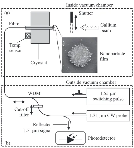
Fig. 1. The experimental setup used to demonstrate optical memory functionality of a film of gallium nanoparticles self-assembled on the end face of an optical fiber. The inset is an scanning electron microscope image of the gallium nanoparticle film on the core of the cleaved optical fiber.
phases with radically different dielectric properties. The state of the nanoparticles is read by a weak optical probe beam, and we show that a single optical pulse can irreversibly switch nanoparticles from a low reflectivity phase into a high reflectivity phase, thus providing mem-ory write functionality. Memmem-ory erase functionality is meanwhile provided by removing the optical probe beam or simply by cooling the film down. Thus, our results show that a resonator-less optical memory element can be created with a nanoparticle undergoing a structural trans-formation.
To demonstrate such memory functionality, a film of gallium nanoparticles deposited onto the end face of an optical fiber was used. The nanoparticles were grown to a median diameter of 50 nm, using the light assisted atomic beam deposition technique as described elsewhere [7]. A film of nanoparticles was grown on the end face of an optical fiber, using the setup schematically illustrated in Fig. 1. This way, the film is ideally positioned for its optical probing and excitation. The fiber supporting the film of nanoparticles was attached to a liquid nitrogen cooled cryostat inside a vacuum chamber, operated at a pressure of 10−6mbar, allowing the temperature of the
film to be varied in the range from 80 to 300 K.
Two lasers were used as light sources in the optical characterization of the nanoparticle film. The first, which was used to probe the state of the nanoparticles by monitoring the reflectivity of the film, was a 1 mW continuous wave (CW) diode laser operating at a wavelength of 1310 nm. The second, which was used to optically excite and switch the nanoparticles, was a pulsed diode laser operating at a wavelength of 1550 nm, generating single optical pulses on demand.
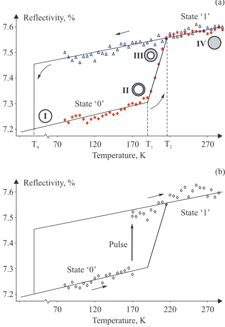
Fig. 2. (a) Dynamic coexistence of structural forms in the gallium nanoparticle film at different stages during the phase transition. Starting from I in a low reflectivity ‘0’ state, the film remains in this memory state until the temperature passes T2(the upper boundary of the phase coexistence domain) after which the film enters and remains in a high reflectivity ‘1’ state. The film only returns to the low reflectivity ‘0’ state on passing below the lower switching temperature T0. The arrows show the hysteresis cycle followed during a complete temperature scan from below T0to above T2and back again. (b) Demonstration of ’memory write’ functionality: switching from the low reflectivity ‘0’ state to the high reflectivity ‘1’ state, using a single laser pulse.
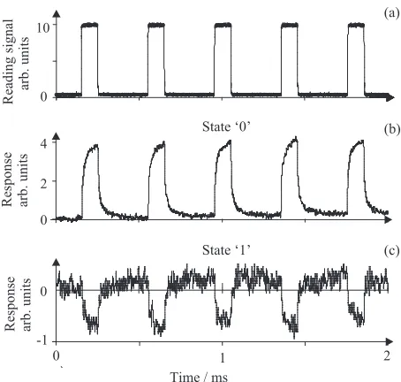
[image:3.612.191.420.80.412.2]Fig. 3. Differential change of reflectance between the bias level and the induced change in the ‘0’ and ‘1’ level. As the pulses of the weak optical probe, shown in (a), excite the nanoparticle film with an energy less than that of a full transition, the reflectance of the low-reflectivity state ‘0’ is positively shifted, as shown in (b). For the high-low-reflectivity state ‘1’, the shift is instead negative as shown in (c), thus providing means to extract a sensitive read-out functionality of the nanoparticle memory.
phase diagram of gallium[8], the states ‘0’ and ‘1’ can be attributed to theβ and liquid phases. In order to demonstrate the memory functionality of the gallium nanoparticle film, one must be able to switch it into the high reflectivity state at a constant temperature. In the present study, this was achieved using a manually triggered 1550 nm pulsed laser, with the sample kept at a constant temperature close to the phase transition, at Tset=170 K. In order to switch the film
from the logic ‘0’ state to the ‘1’ state, a single optical pulse of peak power 13.1 mW and pulse duration 1µs was used to excite the system. After exposure to the optical pulse, the film was found to be locked into the high reflectivity ‘1’ state. Thus, the gallium nanoparticles can be switched by a single optical pulse from the low reflectivity state ‘0’ to the high reflectivity state ‘1’ at a fixed temperature below the lower transition temperature T1, providing memory write functionality (Fig. 2(b)). The written state is maintained until the nanoparticle film is substantially cooled, to a point below T0at which the particles return to the logical ‘0’ level. Such cooling thus provides memory erase functionality.
state, and at a repetition rate that allowed enough time for the system to recover between pulses. With the nanoparticle memory in either the low or high reflectivity state, the reflectivity changes induced by these weak reading pulses can be measured, with the sign of the induced change indicating whether the memory is in the ‘0’ or ‘1’ logic state. In the low reflectivity state, the differential change induced by such pulses is positive, while in the high reflectivity state it is negative.
This principle of operation was experimentally verified using a weak pulsed laser with a peak power of 3 mW, a pulse width of 100µs, and a repetition rate of 2.5 kHz (Fig. 3(a)). The differential reflectivity changes for the low and high reflectivity states ‘0’ and ‘1’ are shown in Figs. 3(b) and 3(c), respectively. By extracting the sign of the induced reflectivity change, one clearly has a distinct and reliable method of reading the memory without affecting its state. The signal-to-noise ratios for these measurements were found to be 49 and 7.8 for the low and high reflectivity states respectively. It should here be emphasized that in contrast to optically bistable memory elements relying on cavity resonances and optical feedback, which in size possess a lower limit roughly of half a wavelength, the memory functionality we here report is directly due to the different properties of reflection of different structural phases, not relying on any interferometrical effect as such.
In conclusion, we have experimentally demonstrated that gallium nanoparticles undergoing light-induced structural transformations possess all of the characteristics necessary to act as rewritable all-optical memory elements. Although a film of nanoparticles was used for this first proof of concept, each particle can potentially act as a single memory bit. By taking the total energy supplied to the gallium film by a writing pulse and dividing it by the estimated number of nanoparticles present in the effective area of the waveguide mode of the fiber, an upper limit on the total energy required to switch a single nanoparticle from state ‘0’ to state ‘1’ of 400 fJ is obtained. This estimate clearly shows the potential for single nanoparticles to provide memory functionality in future nanophotonic devices, operating at very low power levels.