Operational Amplifiers & Linear Integrated Circuits:
Operational Amplifiers & Linear Integrated Circuits:
Theory and Application / 3E
Theory and Application / 3E
Operational Amplifiers & Linear Integrated Circuits:
Operational Amplifiers & Linear Integrated Circuits:
Theory and Application
Theory and Application
by
James M. Fiore
This Operational Amplifiers & Linear Integrated Circuits: Theory and Application, by James M. Fiore is
copyrighted under the terms of a Creative Commons license:
This work is freely redistributable for non-commercial use, share-alike with attribution
Device datasheets and other product information are copyright by their respective owners
Published by James M. Fiore via dissidents
For more information or feedback, contact: James Fiore, Professor
Electrical Engineering Technology Mohawk Valley Community College 1101 Sherman Drive
Utica, NY 13501
For the latest versions and other titles go to
www.mvcc.edu/jfiore or www.dissidents.com
Preface
Preface
Welcome to the third edition of this text! The first edition was written circa 1990 and was published by West Publishing. The title was then purchased by Delmar/Thomson/Cengage some years later and a new edition was written around 2000 (although it was never tagged as a second edition). That version added a companion laboratory manual. In the early 2000s the text went from hard cover to soft cover, and in early 2016, Cengage decided to revert the copyright back to me, the original and singular author. Having already produced a number
of OER (Open Educational Resource) titles including a microcontroller text using the Arduino platform and
numerous laboratory manuals covering DC circuits, AC circuits, Python programming and discrete electronic devices, it was an obvious decision to go the same route with this book. This third edition includes new specialty
ICs and rewrites of certain sections. If you need information on obsolete legacy ICs such as the NE565,
ICL8038, etc., an OER second edition is available (and for you fans of analog computing, Chapter 10 remains).
The OER lab manual to accompany this text has also been updated to the third edition. It features new exercises
and expansions of the existing ones. If you have any questions regarding the text or lab manual, or are interested in contributing to the project, do not hesitate to contact me. Finally, note that the most recent versions of all of
my OER texts and manuals on electronics, circuit analysis and programming may be found at my MVCC web
site as well as my mirror site: www.dissidents.com The original Preface follows, slightly modified.
The goal of this text, as its name implies, is to allow the reader to become proficient in the analysis and design of circuits utilizing modern linear ICs. It progresses from the fundamental circuit building blocks through to analog/digital conversion systems. The text is intended for use in a second year Operational Amplifiers course at the Associate level, or for a junior level course at the Baccalaureate level. In order to make effective use of this text, students should have already taken a course in basic discrete transistor circuits, and have a solid
background in algebra and trigonometry, along with exposure to phasors. Calculus is used in certain sections of the text, but for the most part, its use is kept to a minimum. For students without a calculus background, these sections may be skipped without a loss of continuity. (The sole exception to this being Chapter Ten, Integrators and Differentiators, which hinges upon knowledge of calculus.)
In writing this text, I have tried to make it ideal for both the teacher and the student. Instead of inundating the student with page after page of isolated formulas and collections of disjunct facts and figures, this text relies on building a sound foundation first. While it may take just a little bit longer to “get into” the operational amplifier than a more traditional approach, the initial outlay of time is rewarded with a deeper understanding and better retention of the later material. I tried to avoid creating formulas out of thin air, as is often done for the sake of expediency in technical texts. Instead, I strove to provide sufficient background material and proofs so that the student is never left wondering where particular formulas came from, or worse, coming to the conclusion that they are either too difficult to understand completely, or are somehow “magic”.
The text can be broken into two major sections. The first section, comprised of Chapters One through Six, can be seen as the foundation of the operational amplifier. Here, a methodical, step by step presentation is used to introduce the basic idealized operational amplifier, and eventually examine its practical limitations with great detail. These chapters should be presented in order. The remaining six chapters comprise a selection of popular applications, including voltage regulation, oscillators, and active filters, to name a few. While it is not
There are a few points worth noting about certain chapters. First, Chapter One presents material on decibels, Bode plots, and the differential amplifier, which is the heart of most operational amplifiers. This chapter may be skipped if your curriculum covers these topics in a discrete semiconductor or circuit analysis course. In this case, it is recommended that students scan the chapter in order to familiarize themselves with the nomenclature used later in the text. As part of the focus on fundamentals, a separate chapter on negative feedback (Chapter Three) is presented. This chapter examines the four basic negative feedback connections that might be used with an operational amplifier, and details the action of negative feedback in general. It stresses the popular
series-parallel (VCVS or non-inverting voltage amplifier) form to show how bandwidth, distortion, input impedance,
etc. are affected. Chapter Six presents a variety of modern special purpose devices for specific tasks, such as high load current, programmable operation, and very high speed. An extensive treatment of active filters is given in Chapter Eleven. Unlike many texts which use a “memorize this” approach to this topic, Chapter Eleven strives to explain the underlying operation of the circuits, yet it does so without the more advanced math
requirement of the classical engineering treatment. The final chapter, Chapter Twelve, serves as a bridge between the analog and digital worlds, covering analog to digital to analog conversion schemes. Please bare in mind that entire books have been written on the topics of active filters and analog/digital systems. Chapters Eleven and Twelve are designed as introductions to these topics, not as the final, exhaustive word.
At the beginning of each chapter is a set of chapter objectives. These point out the major items of importance that will be discussed. Following the chapter objectives is an introduction. The introduction sets the stage for the upcoming discussion, and puts the chapter into perspective with the text as a whole. At the end of each chapter is a summary and a set of review questions. The review questions are of a general nature, and are designed to test for retention of circuit and system concepts. Finally, each chapter has a problem set. For most chapters, the problems are broken into four categories: analysis problems, design problems, challenge problems, and
computer simulation (SPICE) problems. An important point here was in including problems of both sufficient
variety and number. An optional coverage extended topic may also be found at the end of many chapters. An extended topic is designed to present extra discussion and detail on a certain portion of a chapter. This allows you to customize the chapter presentation to a certain degree. Not everyone will want to cover every extended topic. Even if they aren't used as part of the normal run of the course, they do allow for interesting side reading, possible outside assignments, and launching points for more involved discussions.
Integrated with the text are examples using popular SPICE-based circuit simulation packages and derivatives
such as the commercial offerings NI Multisim and Orcad PSpice, or free versions such as Texas Instruments'
Finally, there are two elements included in this text which I always longed for when I was a student. First, besides the traditional circuit examples used to explain circuit operation, a number of schematics of have been included to show how a given type of circuit might be used in the real world. It is one thing to read how a precision rectifier works, it is quite another thing to see how one is being used in an audio power amplifier as part of an overload protection scheme.
The second element deals with the writing style of this text. I have tried to be direct and conversational, without being overly cute or “chatty”. The body of this text is not written in a passive formal voice. It is not meant to be impersonal and cold. Instead, it is meant to sound as if someone were explaining the topics to you over your shoulder. It is intended to draw you into the topic, and to hold your attention. Over the years, I have noticed that some people feel that in order to be taken seriously, a topic must be addressed in a detached, almost antiseptic manner. While I will agree that this mindset is crucial in order to perform a good experiment, it does not translate particularly well to textbooks, especially at the undergraduate level. The result, unfortunately, is a thorough but thoroughly unreadable book. If teachers find a text to be uninteresting, it shouldn't be surprising if the students feel the same. I hope that you will find this text to be serious, complete and engaging.
Acknowledgements
Acknowledgements
In a project of this size, there are many people who have done their part to shape the result. Some have done so directly, others indirectly, and still others without knowing that they did anything at all. First, I'd like to thank my wife Karen, family and friends for being such “good eggs” about the project, even if it did mean that I disappeared for hours on end in order to work on it. For their encouragement and assistance, my fellow faculty
members and students. For reverting the copyright back to me so that I could make an OER text, Cengage
Publishing. Finally, I'd like to thank the various IC and equipment manufacturers for providing pertinent data sheets, schematics, and photographs.
For potential authors, this text was created using several free and open software applications including Open
Office and Dia, along with a few utilities I created myself. The filter graphs found in Chapter Eleven were
created using SciDAVis. Screen imagery was often manipulated though the use of XnView.
I cannot say enough about the emerging Open Educational Resource movement and I encourage budding authors to consider this route. While there are (generally) no royalties to be found, having complete control over your own work (versus the “work for hire” classification of typical contracts) is not to be undervalued. Neither should contributions to the profession or the opportunity to work with colleagues be dismissed. Given the practical aspects of the society in which we live, I am not suggesting that people “work for free”. Rather, because part of the mission of institutes of higher learning is to promote and disseminate formalized instruction and information, it is incumbent on those institutions to support their faculty in said quest, whether that be in the form of sabbaticals, release time, stipends or the like.
Finally, it is still no lie to say that I couldn't have completed this project without my personal computers; a stack
of Frank Zappa, Kate Bush, King Crimson, Stravinsky and Bartόk CDs; and the endless stream of healthy and
tasty goodies flowing from Karen's kitchen.
For Karen
“Information is not knowledge, knowledge is not wisdom.”
-Frank Zappa
“Training is not education.”
- Anon
“My hovercraft is full of eels.”
Table of Contents
Table of Contents
Chapter 1: Introductory Concepts and Fundamentals
Chapter 1: Introductory Concepts and Fundamentals
15
15
Chapter Objectives
.
.
.
.
.
.
.
15
1.1 Introduction
.
.
.
.
.
.
.
15
Variable Naming Convention 16
1.2 The Decibel .
.
.
.
.
.
.
.
17
Decibel Representation of Power and Voltage Gains 17
Signal Representation in dBW and dBV 23
Items Of Interest In The Laboratory 25
1.3 Bode Plots .
.
.
.
.
.
.
.
27
Lead Network Gain Response 28
Lead Network Phase Response 31
Lag Network Response 33
Risetime versus Bandwidth 36
1.4 Combining The Elements - Multi-Stage Effects
.
.
.
38
1.5 Circuit Simulations Using Computers
.
.
.
.
40
1.6 The Differential Amplifier .
.
.
.
.
.
43
DC Analysis 43
Input Offset Current and Voltage 46
AC Analysis 46
Common Mode Rejection 53
Current Mirror 55
Summary
.
.
.
.
.
.
.
.
58
Review Questions
.
.
.
.
.
.
.
58
Problem Set
.
.
.
.
.
.
.
.
59
Chapter 2: Operational Amplifier Internals
Chapter 2: Operational Amplifier Internals
63
63
Chapter Objectives
.
.
.
.
.
.
.
63
2.1 Introduction
.
.
.
.
.
.
.
63
2.2 What Is An Op Amp?
.
.
.
.
.
.
63
Block Diagram Of An Op Amp 64
A Simple Op Amp Simulation Model 69
Op Amp Data Sheet and Interpretation 70
2.3 Simple Op Amp Comparator
.
.
.
.
.
74
2.4 Op Amp Manufacture
.
.
.
.
.
.
78
Monolithic Construction 78
Hybrid Construction 80
Summary
.
.
.
.
.
.
.
.
81
Review Questions
.
.
.
.
.
.
.
81
Chapter 3: Negative Feedback
Chapter 3: Negative Feedback
85
85
Chapter Objectives
.
.
.
.
.
.
.
85
3.1 Introduction
.
.
.
.
.
.
.
85
3.2 What Negative Feedback Is and Why We Use It
.
.
.
85
3.3 Basic Concepts
.
.
.
.
.
.
.
86
The Effects of Negative Feedback 87
3.4 The Four Variants of Negative Feedback
.
.
.
.
90
Series-Parallel (SP) 91
SP Impedance Effects 98
Distortion Effects 102 Noise 106 Parallel-Series (PS) 106 PS Impedance Effects 109 Parallel-Parallel (PP) and Series-Series (SS) 111
3.5 Limitations On The Use of Negative Feedback
.
.
.
112
Summary
.
.
.
.
.
.
.
.
113
Review Questions
.
.
.
.
.
.
.
113
Problem Set
.
.
.
.
.
.
.
114
Chapter 4: Basic Op Amp Circuits
Chapter 4: Basic Op Amp Circuits
117
117
Chapter Objectives
.
.
.
.
.
.
.
117
4.1 Introduction
.
.
.
.
.
.
.
117
4.2 Inverting and Non-inverting Amplifiers
.
.
.
.
118
The Non-inverting Voltage Amplifier 118 Inverting Voltage Amplifier 122 Inverting Current-to-Voltage Transducer 126 Non-inverting Voltage-to-Current Transducer 127 Inverting Current Amplifier 130 Summing Amplifiers 133 Non-Inverting Summing Amplifier 136 Differential Amplifier 139 Adder/Subtractor 141 Adjustable Inverter/Non-inverter 142
4.3 Single Supply Biasing
.
.
.
.
.
.
143
4.4 Current Boosting .
.
.
.
.
.
.
146
Summary
.
.
.
.
.
.
.
.
148
Review Questions
.
.
.
.
.
.
.
149
Problem Set
.
.
.
.
.
.
.
149
Chapter 5: Practical Limitations of Op Amp Circuits
Chapter 5: Practical Limitations of Op Amp Circuits
156
156
Chapter Objectives
.
.
.
.
.
.
.
156
5.1 Introduction
.
.
.
.
.
.
.
156
5.2 Frequency Response
.
.
.
.
.
.
156
Low Frequency Limitations 168
5.4 Slew Rate and Power Bandwidth
.
.
.
.
.
169
The Effect of Slew Rate on Pulse Signals 171 The Effect of Slew Rate on Sinusoidal Signals and Power Bandwidth 172 Design Hint 176 Slew Rate and Multiple Stages 177 Non-Compensated Devices 178 Feedforward Compensation 178 De-compensated Devices 179
5.5 Offsets
.
.
.
.
.
.
.
.
180
Offset Sources and Compensation 180
5.6 Drift
.
.
.
.
.
.
.
.
187
5.7 CMRR and PSRR
.
.
.
.
.
.
.
189
5.8 Noise
.
.
.
.
.
.
.
.
191
Summary
.
.
.
.
.
.
.
.
196
Review Questions
.
.
.
.
.
.
.
197
Problem Set
.
.
.
.
.
.
.
.
197
Chapter 6: Specialized Op Amps
Chapter 6: Specialized Op Amps
201
201
Chapter Objectives
.
.
.
.
.
.
.
201
6.1 Introduction
.
.
.
.
.
.
.
201
6.2 Instrumentation Amplifiers .
.
.
.
.
.
202
6.3 Programmable Op Amps .
.
.
.
.
.
211
6.4 Op Amps for High Current, Power, and Voltage Applications
.
214
High Current Devices 215 High Voltage Devices 2186.5 High Speed Amplifiers
.
.
.
.
.
.
219
6.6 Voltage Followers and Buffers
.
.
.
.
.
220
6.7 Operational Transconductance Amplifier .
.
.
.
221
6.8 Norton Amplifier
.
.
.
.
.
.
.
225
6.9 Current Feedback Amplifiers
.
.
.
.
.
232
6.10 Other Specialized Devices
.
.
.
.
.
237
Summary
.
.
.
.
.
.
.
.
238
Review Questions
.
.
.
.
.
.
.
238
Problem Set
.
.
.
.
.
.
.
.
239
Chapter 7: Non-Linear Circuits
Chapter 7: Non-Linear Circuits
243
243
Chapter Objectives
.
.
.
.
.
.
.
243
7.1 Introduction
.
.
.
.
.
.
.
243
7.2 Precision Rectifiers .
.
.
.
.
.
.
244
Peak Detector 248 Precision Full-Wave Rectifier 251
7.3 Wave Shaping
.
.
.
.
.
.
.
254
Active Clampers 254
7.4 Function Generation
.
.
.
.
.
.
262
7.5 Comparators
.
.
.
.
.
.
.
273
7.6 Log and Anti-Log Amplifiers
.
.
.
.
.
282
Four-Quadrant Multiplier 286
7.7 Extended Topic: A Precision Log Amp
.
.
.
.
289
Summary
.
.
.
.
.
.
.
.
292
Review Questions
.
.
.
.
.
.
.
293
Problem Set
.
.
.
.
.
.
.
.
293
Chapter 8: Voltage Regulation
Chapter 8: Voltage Regulation
298
298
Chapter Objectives
.
.
.
.
.
.
.
298
8.1 Introduction
.
.
.
.
.
.
.
298
8.2 The Need For Regulation .
.
.
.
.
.
299
8.3 Linear Regulators
.
.
.
.
.
.
301
Three Terminal Devices 305 Current Boosting 309 Low Dropout Regulators 310 Programmable and Tracking Regulators 310
8.4 Switching Regulators
.
.
.
.
.
.
323
8.5 Heat Sink Usage
.
.
.
.
.
.
.
333
Physical Requirements 334 Thermal Resistance 334
8.6 Extended Topic: Primary Switcher .
.
.
.
.
338
Summary
.
.
.
.
.
.
.
.
339
Review Questions
.
.
.
.
.
.
.
340
Problem Set
.
.
.
.
.
.
.
.
341
Chapter 9: Oscillators and Frequency Generators
Chapter 9: Oscillators and Frequency Generators
344
344
Chapter Objectives
.
.
.
.
.
.
.
344
9.1 Introduction
.
.
.
.
.
.
.
344
9.2 Op Amp Oscillators .
.
.
.
.
.
.
345
Positive Feedback and the Barkhausen Criterion 345 A Basic Oscillator 346 Wien Bridge Oscillator 347 Phase Shift Oscillator 353 Square/Triangle Function Generator 360
9.3 Single Chip Oscillators and Frequency Generators .
.
.
371
Square Wave/Clock Generator 371
Voltage-Controlled Oscillator 373
Phase-Locked Loop 379
555 Timer 382
555 Monostable Operation 383
Summary
.
.
.
.
.
.
.
.
388
Review Questions
.
.
.
.
.
.
.
389
Problem Set
.
.
.
.
.
.
.
.
389
Chapter 10: Integrators and Differentiators
Chapter 10: Integrators and Differentiators
396
396
Chapter Objectives
.
.
.
.
.
.
.
396
10.1 Introduction
.
.
.
.
.
.
.
396
10.2 Integrators
.
.
.
.
.
.
.
397
Accuracy and Usefulness of Integration 399
Optimizing the Integrator 399
Analyzing Integrators with the Time-Continuous Method 403 Analyzing Integrators with the Time-Discrete Method 405
10.3 Differentiators
.
.
.
.
.
.
.
410
Accuracy and Usefulness of Differentiation 411
Optimizing the Differentiator 412
Analyzing Differentiators with the Time-Continuous Method 413 Analyzing Differentiators with the Time-Discrete Method 416
10.4 Analog Computer .
.
.
.
.
.
.
423
10.5 Alternatives to Integrators and Differentiators
.
426
10.6 Extended Topic: Other Integrator and Differentiator Circuits
.
426
Summary
.
.
.
.
.
.
.
.
428
Review Questions
.
.
.
.
.
.
.
429
Problem Set
.
.
.
.
.
.
.
.
430
Chapter 11: Active Filters
Chapter 11: Active Filters
435
435
Chapter Objectives
.
.
.
.
.
.
.
435
11.1 Introduction
.
.
.
.
.
.
.
435
11.2 Filter Types
.
.
.
.
.
.
.
436
11.3 The Use and Advantages of Active Filters .
.
.
.
437
11.4 Filter Order and Poles
.
.
.
.
.
.
438
11.5 Filter Class or Alignment .
.
.
.
.
.
439
Butterworth 441
Bessel 441
Chebyshev 441
Elliptic 443
Other Possibilities 443
11.6 Realizing Practical Filters .
.
.
.
.
.
443
Sallen and Key VCVS Filters 443
Sallen and Key Low-Pass Filters 446
Sallen and Key High-Pass Filters 456
Filters of Higher Order 459
11.7 Band-Pass Filter Realizations
.
.
.
.
.
471
Multiple-Feedback Filters 472
11.8 Notch Filter (Band-Reject) Realizations
.
.
.
.
483
A Note on Component Selection 486
Filter Design Tools 487
11.9 Audio Equalizers .
.
.
.
.
.
.
487
11.10 Switched-Capacitor Filters
.
.
.
.
.
491
11.11 Extended Topic: Voltage-Controlled Filters
.
.
.
495
Summary
.
.
.
.
.
.
.
.
497
Review Questions
.
.
.
.
.
.
.
498
Problem Set
.
.
.
.
.
.
.
.
499
Chapter 12: Analog-to-Digital-to-Analog Conversion
Chapter 12: Analog-to-Digital-to-Analog Conversion
503
503
Chapter Objectives
.
.
.
.
.
.
.
503
12.1 Introduction
.
.
.
.
.
.
.
503
The Advantages and Disadvantages of Working in the Digital Domain 504
12.2 The Sampling Theorem
.
.
.
.
.
.
505
12.3 Resolution and Sampling Rate
.
.
.
.
.
506
12.4 Digital-to-Analog Conversion Techniques .
.
.
.
511
Practical Digital-to-Analog Converter Limits 516
Digital-to-Analog Converter Integrated Circuits 520 Applications of Digital-to-Analog Converter Integrated Circuits 527
12.5 Analog-to-Digital Conversion
.
.
.
.
.
531
Analog-to-Digital Conversion Techniques 535
Analog-to-Digital Converter Integrated Circuits 538 Applications of Analog-to-Digital Converter Integrated Circuits 544
12.6 Extended Topic: Digital Signal Processing .
.
.
.
548
Summary
.
.
.
.
.
.
.
.
551
Review Questions
.
.
.
.
.
.
.
552
Problem Set
.
.
.
.
.
.
.
.
552
Appendices
Appendices
555
555
A: Manufacturer's Data Sheet Links
.
.
.
.
.
555
B: Standard Component Sizes .
.
.
.
.
.
557
C: Answers to Selected Review Questions
.
.
.
.
558
1
1
Introductory Concepts and Fundamentals
Introductory Concepts and Fundamentals
Chapter Learning Objectives
Chapter Learning Objectives
After completing this chapter, you should be able to:
• Convert between ordinary and decibel based power and voltage gains.
• Utilize decibel-based voltage and power measurements during circuit analysis.
• Define and graph a general Bode plot.
• Detail the differences between lead and lag networks, and graph Bode plots for each.
• Combine the effects of several lead and lag networks together in order to determine a system
Bode plot.
• Describe the use of digital computers in the area of circuit simulation.
• Analyze differential amplifiers for a variety of AC characteristics, including single ended and
differential voltage gains.
• Define common-mode gain and common-mode rejection.
• Describe a current mirror and note typical uses for it.
1.1 Introduction
1.1 Introduction
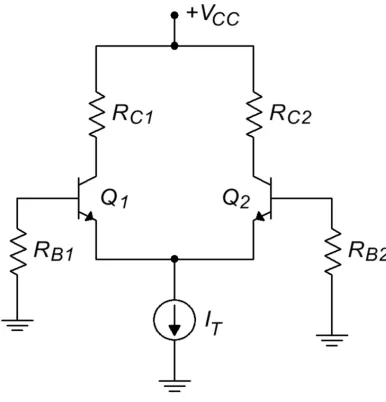
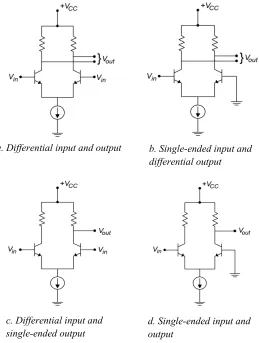
Before we can begin our study of the operational amplifier, it is very important that certain background elements be in place. The purpose of this chapter is to present the very useful analysis concepts and tools associated with the decibel measurement scheme and the frequency domain. We will also be examining the differential amplifier that serves as the heart of most operational amplifiers. With a thorough working knowledge of these items, you will find that circuit design and analysis will proceed at a much quicker and more efficient pace. Consider this chapter as an investment in time, and treat it appropriately.
The decibel measurement scheme is in very wide use, particularly in the field of communications. We will be examining its advantages over the ordinary system of measurement, and how to convert values of one form into the other. One of the more important parameters of a circuit is its frequency response. To this end, we will be looking at the general frequency domain representations of a circuit’s gain and phase. This will include both manual and computer generated analysis and graphing techniques. While our main emphasis will eventually concentrate on application with operational amplifiers, the techniques explored can be applied equally to discrete circuits. Indeed, our initial examples will use simple discrete or black box circuits exclusively.
Variable Naming Convention
Variable Naming Convention
One item that often confuses students of almost any subject is nomenclature. It is important, then, that we decide upon a consistent naming convention at the outset. Throughout this text, we will be examining numerous circuits containing several passive and active components. We will be interested in a variety of parameters and signals. Although we will utilize the standard conventions, such as fc for critical
frequency and Xc for capacitive reactance, a great number of other possibilities exist.
In order to keep confusion to a minimum, we will use the following conventions in our equations for naming devices and signals that haven’t been standardized.
R Resistor (DC, or actual circuit component)
r Resistor (AC equivalent, where phase is 0 or ignored)
C Capacitor
L Inductor
Q Transistor (Bipolar or FET)
D Diode
V Voltage (DC)
v Voltage (AC)
I Current (DC)
i Current (AC)
Resistors, capacitors and inductors are differentiated via a subscript that usually refers to the active device it is connected to. For example, RE is a DC bias resistor
connected to the emitter of a transistor, while rC refers to the AC equivalent
resistance seen at a transistor’s collector. CE refers to a capacitor connected to a
transistor’s emitter lead (most likely a bypass or coupling capacitor). Note that the device related subscripts are always shown in upper case, with one exception: If the resistance or capacitance is part of the device model, the subscript will be shown in lower case to distinguish it from the external circuit components. For example, the AC dynamic resistance of a diode would be called rd. If no active devices are
present, or if several items exist in the circuit, a simple numbering scheme is used, such as R1. In very complex circuits, a specific name will be given to particularly
important components, as in Rsource.
Voltages are normally given a two-letter subscript indicating the nodes at which it is measured. VCE is the DC potential from the collector to the emitter of a transistor,
while vBE indicates the AC signal appearing across a transistor’s base-emitter
junction. A single-letter subscript, as in VB, indicates a potential relative to ground
(in this case, base to ground potential). The exceptions to this rule are power supplies, that are given a double letter subscript indicating the connection point (VCC
is the collector power supply), and particularly important potentials that are directly named, as in vin (AC input voltage) and VR1 (DC voltage appearing across R1). If an
vast majority of op amp circuits that are directly coupled, and thus can amplify both AC and DC signals). Currents are named in a similar way, but generally use a single subscript referring to the measurement node (IC is the DC collector current). All
other items are directly named. By using this scheme, you will always be able to determine whether the item expressed in an equation is a DC or AC equivalent, its approximate circuit location, and other factors about it.
1.2 The Decibel
1.2 The Decibel
Most people are familiar with the term “decibel” in reference to sound pressure. It’s not uncommon to hear someone say something such as “It was 110 decibels at the concert last night, and my ears are still ringing.” This popular use is somewhat inaccurate, but does show that decibels indicate some sort of quantity - in this case, sound pressure level.
Decibel Representation of Power and Voltage Gains
Decibel Representation of Power and Voltage Gains
In its simplest form, the decibel is used to measure some sort of gain, such as power or voltage gain. Unlike the ordinary gain measurements that you may be familiar with, the decibel form is logarithmic. Because of this, it can be very useful for showing ratios of change, as well as absolute change. The base unit is the Bel. To convert an ordinary gain to its Bel counterpart, just take the common log (base 10) of the gain. In equation form:
Bel gain=log10(ordinary gain)
Note that on most hand calculators common log is denoted as “log” while the natural log is given as “ln”. Unfortunately, some programming languages use “log” to indicate natural log and “log10” for common log. More than one student has been bitten by this bug, so be forewarned! As an example, if a circuit produces an output power of 200 milliwatts for an input of 10 milliwatts, we would normally say that it has a power gain of:
G=Pout
Pi n
G=200 mW
10 mW
G=20
For the Bel version, just take the log of this result.
G '=log10G G '=log1020
The Bel gain is 1.3 Bels. The term “Bels” is not a unit in the strict sense of the word (as in “watts”), but is simply used to indicate that this is not an ordinary gain. In contrast, ordinary power and voltage gains are sometimes given units of W/W and V/V to distinguish them from Bel gains. Also, note that the symbol for Bel power gain is G' and not G. All Bel gains are denoted with the following prime (’) notation to avoid confusion. Because Bels tend to be rather large, we typically use one-tenth of a Bel as the norm. The result is the decibel (one-tenth Bel). To convert to decibels, simply multiply the number of Bels by 10. Our gain of 1.3 Bels is equivalent to 13 decibels. The units are commonly shortened to dB. Consequently, we may say:
G '=10 log10G (1.1)
Where the result is in dB
At this point, you may be wondering what the big advantage of the decibel system is. To answer this, recall a few log identities. Normal multiplication becomes addition in the log system, and division becomes subtraction. Likewise, powers and roots become multiplication and division. Because of this, two important things show up. First, ratios of change become constant offsets in the decibel system, and second, the entire range of values diminishes in size. The result is that a very wide range of gains may be represented within a fairly small scope of values, and the corresponding calculations can become quicker. There are a couple of dB values that are useful to remember. With the aid of your hand calculator, it is very easy to show the following:
Factor G’= 10 logdB Value using 10 G
1 0 dB
2 3.01 dB
4 6.02 dB
8 9.03 dB
10 10 dB
We can also look at fractional factors (i.e., losses instead of gains.)
Factor dB Value
0.5 -3.01 dB
0.25 -6.02 dB
0.125 -9.03 dB
0.1 -10 dB
equivalent to 3 dB + 3 dB, or 6 dB. Remember, because we are using logs, multiplication turns into simple addition. In a similar manner, a halving is represented by approximately -3 dB. The negative sign indicates a reduction. To simplify things a bit, think of factors of 2 as ±3 dB, the sign indicating whether you are increasing (multiplying), or decreasing (dividing). As you can see, factors of 10 work out to a very convenient 10 dB. By remembering these two factors, you can often estimate a dB conversion without the use of your calculator. For instance, we could rework our initial conversion problem as follows:
• The amplifier has a gain of 20
• 20 can be written as 2 times 10
• The factor of 2 is 3 dB, the factor of 10 is 10 dB
• The answer must be 3 dB + 10 dB, or 13 dB
• This verifies our earlier result
Time for a few examples.
Example 1.1
An amplifier has a power gain of 800. What is the decibel power gain?
G '=10 log10G G '=10 log10800
G '=10×2.903
G '=29.03dB
We could also use our estimation technique:
• G = 800 = 8∙102
• 8 is equivalent to 3 factors of 2, or 2∙2∙2, and can be expressed as 3 dB +
3 dB + 3 dB, which is, of course, 9 dB
• 102 is equivalent to 2 factors of 10, or 10 dB + 10 dB = 20 dB
• The result is 9 dB + 20 dB, or 29 dB
Note that if the leading digit is not a power of 2, the estimation will not be as precise. For example, if the gain is 850, you know that the decibel gain is just a bit over 29 dB. You also know that it must be less than 30 dB
(1000=103 which is 3 factors of 10, or 30 dB.) As you can see, by using the
Example 1.2
An attenuator reduces signal power by a factor of 10,000. What is this loss expressed in dB?
G '=10 log10
1 10,000
G '=10×(−4)
G '=−40 dB
By using the approximation, we can say,
1
10,000=10
−4
The negative exponent tells us we have a loss (negative dB value), and 4 factors of 10.
G '= −10 dB −10dB −10dB −10 dB
G '= −40dB
Remember, if an increase in signal is produced, the result will be a positive dB value. A decrease in signal will always result in a negative dB value. A signal that is unchanged indicates a gain of unity, or 0 dB.
To convert from dB to ordinary form, just invert the steps; that is, divide by ten and then take the antilog.
G=log−101 G'
10
On most hand calculators, base 10 antilog is denoted as 10x. In most computer
languages, you just raise 10 to the appropriate power, as in G = 10.0^(Gprime / 10.0) (BASIC), or use an exponent function, as in pow(10.0, Gprime / 10.0) (C or
Python).
Example 1.3
An amplifier has a power gain of 23 dB. If the input is 1 mW, what is the output?
G=log−101G '
10
G=log−101
23 10
G=199.5
Therefore, Pout =199.5 ∙ 1 mW, or 199.5 mW
You could also use the approximation technique in reverse. To do this, break up the dB gain in 10 dB and 3 dB chunks:
23dB=3dB+10dB+10dB
Now replace each chunk with the appropriate factor, and multiply them together (remember, when going from log to ordinary form, addition turns into multiplication.)
3dB=2X,10dB=10X , so,
G=2×10×10
G=200
While the approximation technique appears to be slower than the calculator, practice will show otherwise. Being able to quickly estimate dB values can prove to be a very handy skill in the electronics field. This is particularly true in larger, multi-stage designs.
Example 1.4
A three-stage amplifier has gains of 10 dB, 16 dB, and 14 dB per section. What is the total dB gain?
Because dB gains are a log form, just add the individual stage gains to arrive at the system gain.
G 'total=G'1+G '2+G '3 G 'total=10dB+16 dB+14dB
G 'total=40 dB
varies as the square of voltage. In other words, a doubling of voltage will produce a quadrupling of power. If you were to use the same dB conversions, a doubling of voltage would be 3 dB, yet, because the power has quadrupled, this would indicate a 6 dB rise. Consequently, voltage gain (and current gain as well) are treated in a slightly different fashion. We would rather have our doubling of voltage work out to 6 dB, so that it matches the power calculation. The correction factor is very simple. Because power varies as the second power of voltage, the dB form should be twice as large for voltage (remember, exponentiation turns into multiplication when using logs). Applying this factor to equation 1.1 yields:
A 'v=20 log10Av (1.2)
Be careful though, the Bel voltage gain only equals the Bel power gain if the input and output impedances of the system are matched (you may recall from your earlier work that it is quite possible to design a circuit with vastly different voltage and power gains. A voltage follower, for example, exhibits moderate power gain with a voltage gain of unity. It is quite likely that the follower will not exhibit matched impedances.) If we were to recalculate our earlier table of common factors, we would find that a doubling of voltage gain is equivalent to a 6 dB rise, and a ten fold increase is equivalent to a 20 dB rise, twice the size of their power gain counterparts.
Note that current gain may be treated in the same manner as voltage gain (although this is less commonly done in practice).
Example 1.5
An amplifier has an output signal of 2 V for an input of 50 mV. What is A'v?
First find the ordinary gain.
Av= 2
0.05=40
Now convert to dB form.
A 'v=20 log1040
A 'v=20×1.602
A 'v=32.04 dB
The approximation technique yields 40=2∙2∙10, or 6 dB + 6 dB + 20 dB = 32 dB
To convert A'v to A, reverse the process.
Av=log10 −1A 'v
Example 1.6
An amplifier has a gain of 26 dB. If the input signal is 10 mV, what is the output?
Av=log10−1A'v
20
Av=log10−12620
Av=19.95
Vout=AvVi n
Vout=19.95×10 mV
The final point to note in this section is that, as in the case of power gain, a negative dB value indicates a loss. Therefore, a 2:1 voltage divider would have a gain of -6 dB.
Signal Representation in dBW and dBV
Signal Representation in dBW and dBV
As you can see from the preceding section, it is possible to spend considerable time converting between decibel gains and ordinary voltages and powers. Because the decibel form does offer advantages for gain measurement, it would make sense to use a decibel form for power and voltage levels as well. This is a relatively
straightforward process. There is no reason why we can’t express a power or voltage in a logarithmic form. Because a dB value just indicates a ratio, all we need to do is decide on a reference (i.e., a comparative base for the ratio). For power
measurements, a likely choice would be 1 watt. In other words, we can describe a power as being a certain number of dB above or below 1 watt. Positive values will indicate powers greater than 1 watt, while negative values will indicate powers less than 1 watt. In general equation form:
P '=10log10 P
reference (1.3)
Example 1.7
A power amplifier has a maximum output of 120 W. What is this power in dBW?
P '=10log10
P
1 Watt
P '=10log10
120 W 1W
P '=20.8 dBW
There is nothing sacred about the 1 watt reference, short of its convenience. We could just as easily choose a different reference. Other common reference points are 1 milliwatt (dBm) and 1 femtowatt (dBf). Obviously, dBf is used for very low signal levels, such as those coming from an antenna. dBm is in very wide use in the communications industry. To use these other references, just divide the given power by the new reference.
Example 1.8
A small personal audio tape player delivers 200 mW to its headphones. What is this output power in dBW, and in dBm?
For an answer in units of dBW, use the 1 watt reference
P '=10 log10 P
1Watt
P '=10 log10
200 mW 1 W
P '=−7 dBW
For units of dBm, use a 1 milliwatt reference
P '=10 log10
P
1Watt
P '=10 log10
200 mW 1 mW
P '=23 dBm
In order to transfer a dBW or similar value into watts, reverse the process.
P=log10−1P '
10×reference
Example 1.9
A studio microphone produces a 12 dBm signal while recording normal speech. What is the output power in watts?
P=log10−1P '
10×reference
P=log10−1
12dBm
10 ×1mW
P=15.8mW=0.0158 W
For voltages, we can use a similar system. A logical reference is 1 V, with the resulting units being dBV. As before, these voltage measurements will use a multiplier of 20 instead of 10.
V '=20log10 V
reference (1.4)
Example 1.10
A test oscillator produces a 2 V signal. What is this value in dBV?
V '=20log10
V reference V '=20log102 V
1 V
V '=6.02dB
Example 1.11
A computer disk read/write amplifier exhibits a gain of 35 dB. If the input signal is -42 dBV, what is the output signal?
V 'out=V 'i n+A'v
V 'out=−42 dBV+35dB
V 'out=−7 dBV
Note that the final units are dBV and not dB, thus indicating a voltage and not merely a gain.
Example 1.12
A guitar power amp needs an input of 20 dBm to achieve an output of 25 dBW. What is the gain of the amplifier in dB?
First, it is necessary to convert the power readings so that they share the same reference unit. Because dBm represents a reference 30 dB smaller than the dBW reference, just subtract 30 dB to compensate.
20 dBm=−10 dBW
G '=P 'out−P 'i n
G '=25dBW−(−10 dBW)
G '=35 dB
Note that the units are dB and not dBW. This is very important! Saying that the gain is “so many” dBW is the same as saying the gain is “so many” watts. Obviously, gains are “pure” numbers and do not carry units such as watts or volts.
Items Of Interest In The Laboratory
Items Of Interest In The Laboratory
When using a digital meter on a dBV scale it is possible to “underflow” the meter if the signal is too weak. This will happen if you try to measure around zero volts, for example. If you attempt to calculate the corresponding dBV value, your calculator will probably show “error”. The effective value is negative infinite dBV. The meter will certainly have a hard time showing this value! Another item of interest revolves around the use of dBm measurements. It is common to use a voltmeter to make dBm measurements, in lieu of a wattmeter. While the connections are considerably simpler, a voltmeter cannot measure power. How is this accomplished then? Well, as long as the circuit impedance is known, power can be derived from a voltage measurement. A common impedance in communication systems (such as recording studios) is 600 Ω, so a meter can be calibrated to give correct dBm readings by using Power Law. If this meter is used on a non-600 Ω circuit, the readings will no longer reflect accurate dBm values (but will still properly reflect relative changes in dB).
1.3 Bode Plots
1.3 Bode Plots
The Bode plot is a graphical response prediction technique that is useful for both
circuit design and analysis. It is named after Hendrik Wade Bode, an American
engineer known for his work in control systems theory and telecommunications. A Bode plot is, in actuality, a pair of plots: One graphs the gain of a system versus frequency, while the other details the circuit phase versus frequency. Both of these items are very important in the design of well-behaved, optimal operational amplifier circuits.
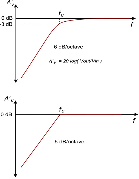
Generally, Bode plots are drawn with logarithmic frequency axes, a decibel gain axis, and a phase axis in degrees. First, let’s take a look at the gain plot. A typical gain plot is shown Figure 1.2.
10 dB -6 dB 15 dB
8 dBm 18 dBm 12 dBm 27 dBm
Figure 1.1
Note how the plot is relatively flat in the middle, or midband, region. The gain value in this region is known as the midband gain. At either extreme of the midband region, the gain begins to decrease. The gain plot shows two important frequencies,
f1 and f2. f1 is the lower break frequency while f2 is the upper break frequency. The
gain at the break frequencies is 3 dB less than the midband gain. These frequencies are also known as the half-power points, or corner frequencies. Normally, amplifiers are only used for signals between f1 and f2. The exact shape of the rolloff regions will
depend on the design of the circuit. It is possible to design amplifiers with no lower break frequency (i.e., a DC amplifier), however, all amplifiers will exhibit an upper break. The break points are caused by the presence of circuit reactances, typically coupling and stray capacitances. The gain plot is a summation of the midband response with the upper and lower frequency limiting networks. Let’s take a look at the lower break, f1.
Lead Network Gain Response
Lead Network Gain Response
Reduction in low frequency gain is caused by lead networks. A generic lead network is shown in Figure 1.3. It gets its name from the fact that the output voltage
developed across R leads the input. At very high frequencies the circuit will be essentially resistive. Conceptually, think of this as a simple voltage divider. The divider ratio depends on the reactance of C. As the input frequency drops, Xc
increases. This makes Vout decrease. At very high frequencies, where Xc<<R, Vout is
approximately equal to Vin. This can be seen graphically in Figure 1.4. The break
frequency (i.e., the frequency at which the signal has decreased by 3 dB) is found via the standard equation
fc= 1 2π R C
Figure 1.2
Gain plot
f A'v
A'midband
f1 midband f2
Figure 1.3
The response below fc will be a straight line if a decibel gain axis and a logarithmic
frequency axis are used. This makes for very quick and convenient sketching of circuit response. The slope of this line is 6 dB per octave (an octave is a doubling or
halving of frequency, e.g., 800 Hz is 3 octaves above 100 Hz).1 This range covers a
factor of two in frequency. This slope may also be expressed as 20 dB per decade, where a decade is a factor of 10 in frequency. With reasonable accuracy, this curve
may be approximated as two line segments, called asymptotes, as shown in Figure
1.5. The shape of this curve is the same for any lead network. Because of this, it is very easy to find the approximate gain at any given frequency as long as fc is known.
It is not necessary to go through reactance and phasor calculations. To create a general response equation, start with the voltage divider rule to find the gain:
Vout Vi n
= R
R−j Xc
Vout
Vi n =
R∠0
√
R2+Xc 2∠−arctanXc
R
1 The term octave is borrowed from the field of music. It gets its name from the fact that there are eight notes in the standard western scale: do-re-me-fa-so-la-ti-do.
f
A'v
-3 dB
fc 0 dB
6 dB/octave
[image:29.612.122.367.60.374.2]A'v = 20 log( Vout/Vin )
Figure 1.4
Lead gain plot (exact)
f
A'v
fc
0 dB
6 dB/octave
Figure 1.5
The magnitude of this is,
∣Av∣= R
√
R2+Xc2
∣Av∣= 1
√
1+Xc2
R2
(1.5)
Recalling that,
f
c=
1
2
π R C
we may say,
R= 1
2π fcC
For any frequency of interest, f,
Xc= 1
2π f C
Equating the two preceding equations yields,
fc f =
Xc
R (1.6)
Substituting equation 1.6 in equation 1.5 gives,
Av= 1
√
1+ fc2
f2
(1.7)
To express A
v in dB, substitute equation 1.7 into equation 1.2
A 'v=20 log10 1
√
1+ fc2
After simplification, the final result is:
A 'v=−10 log10
(
1+ fc2
f2
)
(1.8)Where
fc is the critical frequency,
f is the frequency of interest,
A'v is the decibel gain at the frequency of interest.
Example 1.13
An amplifier has a lower break frequency of 40 Hz. How much gain is lost at 10 Hz?
A 'v=−10 log10
(
1+fc2
f2
)
A 'v=−10 log10
(
1+402
102
)
A 'v=−12.3 dB
In other words, the gain is 12.3 dB lower than it is in the midband. Note that 10 Hz is 2 octaves below the break frequency. Because the cutoff slope is 6 dB per octave, each octave loses 6 dB. Therefore, the approximate result is -12 dB, which double-checks the exact result. Without the lead network, the gain would stay at 0 dB all the way down to DC (0 Hz.)
Lead Network Phase Response
Lead Network Phase Response
At very low frequencies, the circuit of Figure 1.3 is largely capacitive. Because of this, the output voltage developed across R leads by 90 degrees. At very high frequencies the circuit will be largely resistive. At this point Vout will be in phase
with Vin. At the critical frequency, Vout will lead by 45 degrees. A general phase
graph is shown in Figure 1.6. As with the gain plot, the phase plot shape is the same for any lead network. The general phase equation may be obtained from the voltage divider:
Vout Vi n
= R
R−j Xc
Vout
Vi n =
R∠0
√
R2+Xc 2∠−arctan Xc
The phase portion of this is,
θ=arctan Xc
R
By using equation 1.6, this simplifies to,
θ=arctan fc
f (1.9)
Where
fc is the critical frequency,
f is the frequency of interest,
θ is the phase angle at the frequency of interest.
Often, an approximation such as Figure 1.7 used in place of 1.6. By using equation 1.9, you can show that the approximation is off by no more than 6 degrees at the corners.
f
θ
90°
.1fc fc 10fc
45°
0°
f θ
90°
.1fc fc 10fc
45°
0°
Figure 1.7
Lead phase (approximate)
Figure 1.6
Example 1.14
A telephone amplifier has a lower break frequency of 120 Hz. What is the phase response one decade below and one decade above?
One decade below 120 Hz is 12 Hz, while one decade above is 1.2 kHz.
θ=arctan fc
f θ=arctan120 Hz
12Hz
θ=84.3degrees one decade below fc (i.e, approaching 90 degrees)
θ=arctan 120 Hz
1.2 kHz
θ=5.71degrees one decade above fc (i.e., approaching 0 degrees)
Remember, if an amplifier is direct-coupled, and has no lead networks, the phase will remain at 0 degrees right back to 0 Hz (DC).
Lag Network Response
Lag Network Response
Unlike its lead network counterpart, all amplifiers will contain lag networks. In essence, it’s little more than an inverted lead network. As you can see from Figure 1.8, it simply transposes the R and C locations. Because of this, the response tends to be inverted as well. In terms of gain, Xc is very large at low frequencies, and thus
Vout equals Vin. At high frequencies, Xc decreases, and Vout falls. The break point
occurs when Xc equals R. The general gain plot is shown in Figure 1.9. Like the lead
network response, the slope of this curve is -6 dB per octave (or -20 dB per decade.) Note that the slope is negative instead of positive. A straight-line approximation is shown in Figure 1.10. We can derive a general gain equation for this circuit in virtually the same manner as we did for the lead network. The derivation is left as an exercise.
A 'v=−10 log10
(
1+f2
fc2
)
(1.10)Where
fc is the critical frequency,
f is the frequency of interest,
A'v is the decibel gain at the frequency of interest.
Figure 1.8
Note that this equation is almost the same as equation 1.8. The only difference is that
f and fc have been transposed.
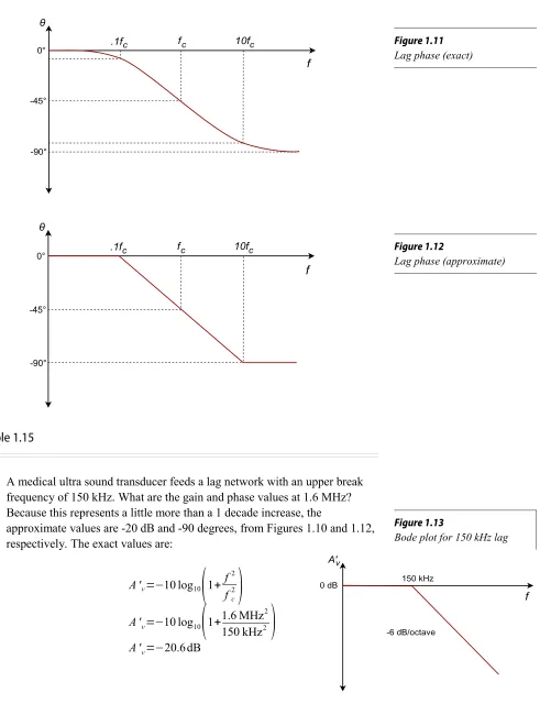
In a similar vein, we may examine the phase response. At very low frequencies, the circuit is basically capacitive. Because the output is taken across C, Vout will be in
phase with Vin. At very high frequencies, the circuit is essentially resistive.
Consequently, the output voltage across C will lag by 90 degrees. At the break
frequency the phase will be -45 degrees. A general phase plot is shown in Figure 1.11, with the approximate response detailed in Figure 1.12. As with the lead network,we may derive a phase equation. Again, the exact steps are very similar, and left as an exercise.
θ=−90+arctan fc
f (1.11)
Where
fc is the critical frequency,
f is the frequency of interest,
θ is the phase angle at the frequency of interest.
f
A'vf
c 0 dB [image:34.612.130.359.124.446.2]-6 dB/octave
Figure 1.9
Lag gain (exact)
Figure 1.10
Lag gain (approximate)
f
A'v-3 dB
f
c 0 dBExample 1.15
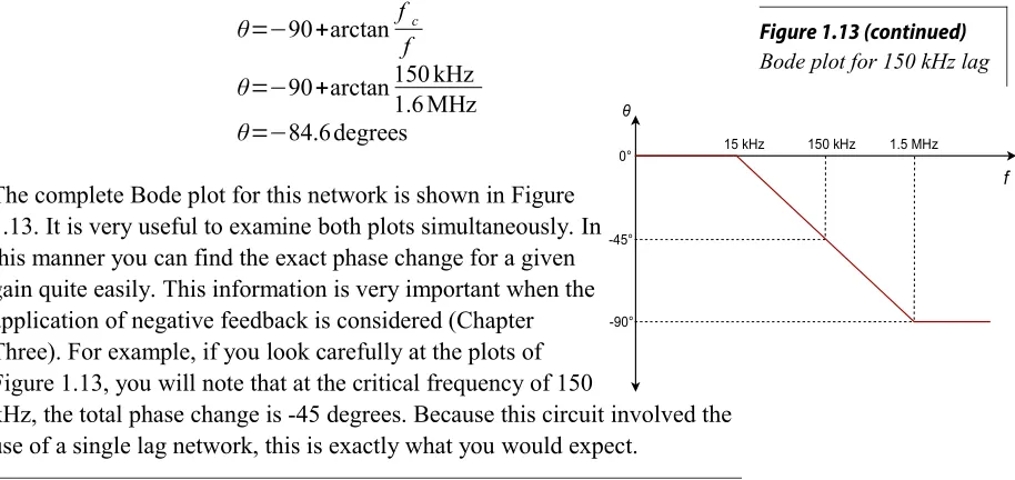
A medical ultra sound transducer feeds a lag network with an upper break frequency of 150 kHz. What are the gain and phase values at 1.6 MHz? Because this represents a little more than a 1 decade increase, the
approximate values are -20 dB and -90 degrees, from Figures 1.10 and 1.12, respectively. The exact values are:
A 'v=−10 log10
(
1+f2
fc 2
)
A 'v=−10 log10
(
1+1.6 MHz2
150 kHz2
)
A 'v=−20.6dB
f
θ
0° .1fc fc 10fc
-45°
-90°
f θ
0° .1fc fc 10fc
-45°
-90°
Figure 1.11
[image:35.612.88.579.53.703.2]Lag phase (exact)
Figure 1.12
Lag phase (approximate)
Figure 1.13
Bode plot for 150 kHz lag
f A'v
150 kHz 0 dB
θ=−90+arctan fc
f
θ=−90+arctan 150 kHz
1.6 MHz
θ=−84.6degrees
The complete Bode plot for this network is shown in Figure 1.13. It is very useful to examine both plots simultaneously. In this manner you can find the exact phase change for a given gain quite easily. This information is very important when the application of negative feedback is considered (Chapter Three). For example, if you look carefully at the plots of Figure 1.13, you will note that at the critical frequency of 150
kHz, the total phase change is -45 degrees. Because this circuit involved the use of a single lag network, this is exactly what you would expect.
Risetime versus Bandwidth
Risetime versus Bandwidth
For pulse-type signals, the speed of an amplifier is often expressed in terms of its
risetime. If a square pulse such as Figure 1.14a is passed into a simple lag network, the capacitor charging effect will produce a rounded variation, as seen in Figure 1.14b. This effect places an upper limit on the duration of pulses that a given amplifier can handle without producing excessive distortion.
By definition, risetime is the amount of time it takes for the signal to traverse from 10% to 90% of the peak value of the pulse. The shape of this pulse is defined by the standard capacitor charge equation examined in earlier course work, and is valid for any system with a single clearly dominant lag network.
Vout=Vpeak
(
1−ϵ−t
RC
)
(1.12)t
Vpeak
t0
Figure 1.14a
Pulse-risetime effect: Input to network
f
θ
0° -45° -90°
150 kHz
15 kHz 1.5 MHz
Figure 1.13 (continued)
[image:36.612.98.555.59.275.2]In order to find the time internal from the initial starting point to the 10% point, set
Vout to 0.1Vpeak in equation 1.12 and solve for t1 .
0.1Vpeak=Vpeak
(
1−ϵ −t1RC
)
0.1Vpeak=Vpeak−Vpeakϵ
−t1
RC
0.9Vpeak=Vpeakϵ
−t1
RC
0.9=ϵ
−t1
RC
log 0.9=−t1
R C
t1=0.105RC (1.13)
To find the interval up to the 90% point, follow the same technique using 0.9Vpeak .
Doing so yields
t2=2.303RC (1.14)
The risetime, Tr, is the difference between t1 and t2
Tr=t1−t2
Tr=2.303R C−0.105RC
Tr≈2.2R C (1.15)
Equation 1.15 ties the risetime to the lag network’s R and C values. These same values also set the critical frequency f2. By combining equation 1.15 with basic
critical frequency relationship, we can derive an equation relating f2 to Tr.
f2= 1
2π RC
Solving 1.15 in terms of RC, and substituting yields
t
Vpeak
t0 t1 t2
.1Vpeak .9Vpeak
Figure 1.14b
f
2=
2.2
2
π T
rf2=0.35
Tr (1.16)
Where
f2 is the upper critical frequency,
Tr is the risetime of the output pulse.
Example 1.16
Determine the risetime for a lag network critical at 100 kHz.
f2=0.35
Tr Tr=0.35f
2
Tr= 0.35
100 kHz
Tr=3.5μs
1.4 Combining the Elements - Multi-Stage Effects
1.4 Combining the Elements - Multi-Stage Effects
A complete gain or phase plot combines three elements: (1) the midband response, (2) the lead response, and (3) the lag response. Normally, a particular design will contain multiple lead and lag networks. The complete response is the summation of the individual responses. For this reason, it is useful to find the dominant lead and lag networks. These are the networks that affect the midband response first. For lead networks, the dominant one will be the one with the highest fc . Conversely, the
dominant lag network will be the one with the lowest fc . It is very common to
approximate the complete system response by drawing straight-line segments such as those given in Figures 1.5 and 1.10. The process goes something like this:
• Locate all fc s on the frequency axis.
• Draw a straight line between the dominant lag and lead fc s at the
midband gain. If the system does not contain any lead networks, continue the midband gain line down to DC.
• Draw a 6 dB per octave slope between the dominant lead and the
next lower lead network.
the third fc , the slope should be 18 dB per octave, after the fourth,
24 dB per octave, and so on.
• Draw a -6 dB per octave slope between the dominant lag fc and the
next highest fc . Again, the effects are cumulative, so increase the
slope by -6 dB at every new fc .
Example 1.17
Draw the Bode gain plot for the following amplifier: A'v midband = 26 dB,
one lead network critical at 200 Hz, one lag network critical at 10 kHz, and another lag network critical at 30 kHz.
The dominant lag network is 10 kHz. There is only one lead network, so it’s dominant by default.
• Draw a straight line between 200 Hz and 10 kHz at an
amplitude of 26 dB.
• Draw a 6 dB per octave slope below 200 Hz. To do this,
drop down one octave (100 Hz) and subtract 6 dB from the present gain (26 dB - 6dB = 20 dB.) The line will start at the point 200 Hz/26 dB, and pass through the point 100 Hz/20 dB. Because there are no other lead networks, this line may be extended to the left edge of the graph.
• Draw a -6 dB per octave slope between 10 kHz and 30 kHz.
The construction point will be 20 kHz/20 dB. Continue this line to 30 kHz. The gain at the 30 kHz intersection should be around 16 dB. The slope above this second fc will be -12
dB per octave. Therefore, the second construction point should be at 60 kHz/4 dB (one octave above 30 kHz, and 12 dB down from the 30 kHz gain). Because this is the final lag network, this line may be extended to the right edge of the graph.
There is one item that should be noted before we leave this section, and that is the concept of narrowing. Narrowing occurs when two or more networks share similar critical frequencies, and one of them is a dominant network. The result is that the true -3 dB breakpoints may be altered. Here is an extreme example. Assume that a circuit has two lag networks, both critical at 1 MHz. A Bode plot would indicate that the breakpoint is 1 MHz. This is not really true. Remember, the effects of lead and lag networks are cumulative. Because each network produces a 3 dB loss at 1 MHz, the net loss at this frequency is actually 6 dB. The true -3 dB point will have been shifted. The Bode plot only gives you the approximate shape of the response.
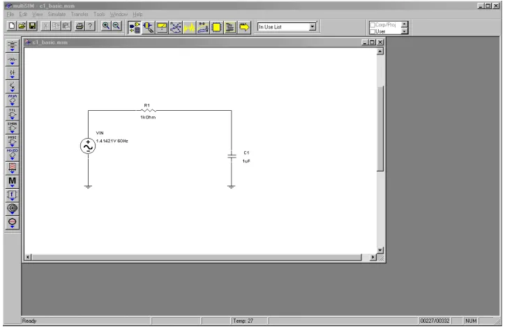
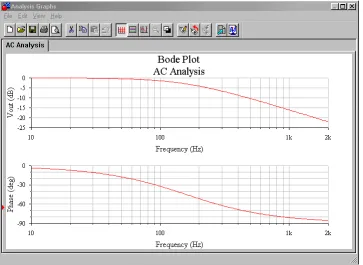
1.5 Circuit Simulations Using Computers
1.5 Circuit Simulations Using Computers
With the advent of low cost personal computers, there are many alternatives to hand sketching of plots. One method involves the use of commercial or public domain software packages designed for circuit anal