Int. J. Electrochem. Sci., 7 (2012) 1785 - 1801
International Journal of
ELECTROCHEMICAL
SCIENCE
www.electrochemsci.orgOptimization of Planar Three-Electrode Systems for Redox
System Detection
Jan Prasek1,2, Libuse Trnkova2,3, Imrich Gablech1, Petra Businova1, Jana Drbohlavova1,2, Jana Chomoucka1,2, Vojtech Adam2,3, Rene Kizek2,3, Jaromir Hubalek1,2*
1
Department of Microelectronics, Faculty of Electrical Engineering and Communication, Brno University of Technology, Technicka 3058/10, CZ-616 00 Brno, Czech Republic, European Union 2
Department of Chemistry and Biochemistry, Faculty of Agronomy, Mendel University in Brno, Zemedelska 1, CZ-613 00 Brno, Czech Republic, European Union
3
Central European Institute of Technology, Brno University of Technology, Technicka 3058/10, CZ-616 00 Brno, Czech Republic, European Union
*
E-mail: [email protected]
Received: 17 July 2011 / Accepted: 23 November 2011 / Published: 1 March 2012
Numerous analytical, bioanalytical, biochemical and biological instruments have been developed for determination of specific and/or group of compounds, species, cells even organisms, but most of them suffer from the impossibility to miniaturize these instruments in spite of the fact that they have many other advantages. Due to the above-mentioned facts developing and suggesting of simple analytical instruments, methods and procedures with low detection limits and providing on-line and in situ monitoring of environment are needed. In this study, we show testing and optimizing of some important features of screen-printed electrodes, which should be considered before their designing, fabrication and applications for low-cost electrochemical analysis in-situ, because we found that areas as well as materials of auxiliary and reference electrode can markedly influence of current response and, therefore, markedly influence detection limit of our thick-film three-electrode microsensor. Finally, there was also confirmed, that these three-electrode screen-printed planar electrode systems could be used for high scan rate electrochemical detection of selected species without any significant output current response change in comparison to standard-like non-planar three-electrode system.
Keywords: Electrochemistry; Planar electrode; Electrode system; Sensor; Thick-film electrode; Electrochemical analysis; Voltammetry
1. INTRODUCTION
assessing both the extent (hazard) and probability (risk) environmental contamination [1]. Numerous analytical, bioanalytical, biochemical and biological instruments have been developed for determination of specific and/or group of compounds, species, cells even organisms, but most of them suffer from the impossibility to miniaturize these instruments in spite of the fact that they have many other advantages. Due to the above-mentioned facts developing and suggesting of simple analytical instruments, methods and procedures with low detection limits and providing on-line and in situ monitoring of environment are needed [2]. Among very sensitive analytical methods for detection of various analytes including metal ions [3-10], peptides [11-16], proteins [17-29], nucleic acids [30-42] and others [43,44] belong the electrochemical ones [11,45-48]. The classic instruments are consisted of potentiostat/galvanostat with electrochemical cell including three electrodes (working, reference and auxiliary). As the working electrode, hanging mercury drop electrode (HMDE) is commonly used [49]. HMDE can be also modified by biologically active substances to improve sensitivity or selectivity of heavy metal ions detection [48,50-55]. Due to adverse effects of Hg(II) and many restrictions for usage of this metal, carbon electrodes has been found as an alternative [56-63]. As we mentioned above the trend of the analytical techniques is to miniaturize the whole instrument, in which carbon electrodes have much more advantages compared to HMDE [64-67].
The miniaturized planar solid electrode systems (sensors) could be fabricated using several methods. One of them is thick-film technology (TFT), [68,69] which was primarily used for fabrication of hybrid electronic circuits. Due to the improvement of surface mount technology in the end of 1980s, TFT started to be used for some other applications, which opened wide possibilities in fabrication of sensors, biosensors, displays, heater elements, etc. The advantage of standard TFT is a variability of used materials, low-cost production, flexibility, accessibility, non-vacuum and ecological friendly fabrication process, good reproducibility, good compatibility with electronic devices and circuits, good mechanical and electrical resistivity and good thermal conductivity of the substrates. Screen-printed carbon electrodes as a product of TFT belong to the most convincing carbon electrodes to be used for in situ environmental analysis [70-74]. Screen-printed electrodes have been successfully used for detection of various gasses [75-80], glucose [81-83], heavy metals [84-90], hydrogen peroxide [91-93], DNA [94-98], methyl parathion [99], phenol in soil sample [100], sildenafil in Viagra tablets [101], and also for blood analysis [102-105].
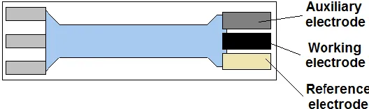
[image:3.596.165.429.182.260.2]
auxiliary electrodes on the output anodic and cathodic current response and half wave potentials voltage shift in standard electrochemical couple of potassium ferrocyanide and ferricyanide solution. Further, we optimized material to prepare the electrodes. The third part of this study was devoted to comparison of planar electrochemical system (sensor) with standard-like non-planar electrodes arrangement.
Figure 1. Screen-printed voltammetric sensor topology.
2. EXPERIMENTAL PART
2.1 Chemicals
Solution of 0.05 mol/L potassium ferrocyanide K4Fe(CN6) and 0.05 mol/L potassium ferricyanide K3Fe(CN6) in 0.1 mol/L KCl in volume ratio 1:1, pH 5.2 and 0.2 M KCl aqueous solution at pH 2 (acidified with HCl) were prepared. All used chemicals of ACS purity were purchased from Sigma-Aldrich Chemical Corp. (USA) unless noted otherwise. Deionized water underwent demineralization by reverse osmosis using the instrument Aqua Osmotic 02 (Aqua Osmotic, Czech Republic) and then it was subsequently purified using Millipore Direct-Q Water Purification System (Millipore Corp., USA, 18 MΏ) – MiliQ water. The pH value was measured using inoLab controlled by the personal computer program (MultiLab Pilot; WTW, Germany).
2.2 Electrochemical measurements
platinum AE (6.0343.000, Metrohm, Switzerland) and an Ag/AgCl RE (6.0726.100, Metrohm, Switzerland).
The experiment with RE material was performed against standard gold WE (UMMAUR11, Sycopel Scientific Limited, UK) and platinum auxiliary electrode (UMMPTB11, Sycopel Scientific Limited, UK). RE Theta 403 (Electrochemical detectors, Turnov, Czech Republic) was used as standard RE for comparison. All experiments were done in a 10 ml voltammetric thermostatic cell (25 °C) equipped with thermostat Petite Fleur (Huber GmbH, Germany) at scan rate 20 mV/s and potential range from -300 to 600 mV.
The experiment with planarity was performed in planar and standard-like non-planar configuration. In the planar system configuration all electrodes from one three-electrode planar system were connected. In non-planar system configuration WE from one against RE and AE from second planar electrochemical system in distance of 5 mm was connected. The measurements were done in ferro-ferricyanide solution diluted to concentration of 0.5 mmol/L and scan rate 160 mV/s.
2.3 Electrode system 2.3.1 Fabrication
All TFT electrode systems were screen-printed on alumina substrates using Aurel C880 semiautomatic screen-printer (Aurel Automation, Italy) and fired using BTU fast fire furnace for thick film processing (BTU, USA). The conductive layer was fabricated from AgPdPt based paste (ESL 9562-G). The protective layer was fabricated from dielectric paste (ESL 4917). Auxiliary electrode was fabricated from Pt based paste (ESL 5545). All cermet pastes were obtained from ESL ElectroScience Europe, UK and fired at 850 °C according the recommended values in products datasheets. The working electrodes were screen-printed using special carbon based conductive paste for electrodes of electrochemical sensors (DuPont BQ221) from DuPont Company (DuPont, USA) and cured at 130 °C for 10 minutes according to datasheet. The reference electrodes for the first two and the fourth experiments were screen-printed using special polymer Ag/AgCl paste (DuPont 5874, Ag:AgCl ratio 65:35) and dried at 120 °C for 5 minutes. Reference electrodes for the third experiment were screen-printed using two polymer Ag/AgCl pastes (DuPont 5874, Ag:AgCl ratio 65:35 and DuPont 5870, Ag:AgCl ratio 80:20) and the rest using silver based paste (ESL 9912-K). The electrochemically coated AgCl RE were prepared using electrochemical reoxidization of silver based RE in 0.2 M KCl [106] against platinum auxiliary electrode (UMMPTB11, Sycopel Scientific Limited, UK) and Ag/AgCl RE Theta 403 (Electrochemical detectors, Turnov, Czech Republic), but some of the TFT Ag paste based REs were used as the underlay.
2.3.2 Characterization
microscopy (SEM) of fabricated samples was performed by Tescan Mira II microscope (Tescan, Czech Republic) controlled by standard PC equipped with MIRATC software version 3.5.11.0. The beam energy was set to 5 kV and the in-beam secondary electrons detector was used for analysis. The chamber pressure was 9×10⁻³
Pa and the ambient chamber temperature was 25 °C.
3. RESULTS AND DISCUSSION
3.1 Design of the study
In the first part of this study, the change of geometrical size of the reference and auxiliary electrodes and its influence to the output anodic and cathodic current response and half wave potentials voltage shift in standard electrochemical couple of potassium ferrocyanide and ferricyanide solution were investigated. One of them was done for the change of RE geometrical size and the second for the change of AE geometrical size, because these two areas could be changed during the electrode design. The second part of this study was devoted to the experiment for searching of suitable material for RE using the same evaluation method. The third part of this study was devoted to comparison of planar electrochemical system (sensor) with standard-like non-planar electrodes arrangement. Therefore two sets of differently sized electrodes for the first, one set of electrodes for the second and another set of electrodes for the third part of this study were designed and fabricated as it is mentioned in Experimental section.
3.2 Electrodes design and fabrication
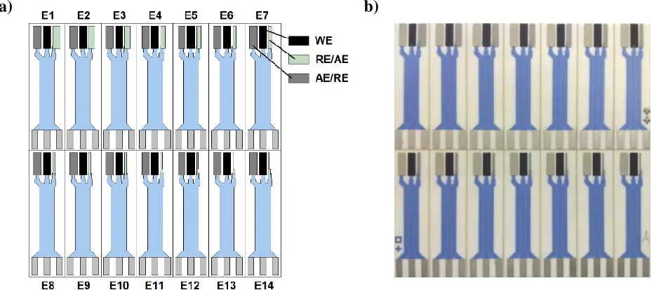
Design of new three-electrode systems used for all experiments came out from the planar voltammetric electrochemical three-electrode screen-printed electrochemical system (sensor) with strip electrodes, which is shown in Fig. 1. The size of the sensor substrate was chosen to be compatible with standard size of printed electrodes used in our laboratory [60], which dimension (7.2 × 25.4 mm) is given by dividing of the standard alumina substrate used in TFT (2×2” in this case) to equal electrode substrates.
and the strip electrode length was 4.5 mm. WE was placed in the middle between RE and AE. All designed electrode systems are shown in Fig. 2a. The designed geometrical areas of AE and RE and their ratio against WE are summarized in Tables 1 and 2, respectively. There were fabricated ten sets containing fourteen changed electrode systems and used for measurements according to Fig. 2a. The same electrodes design was used for variable REs or AEs design, but the RE and AE electrodes positions were swapped during the printing process. Fabricated substrate containing fourteen deposited electrode systems with various AE is shown in Fig. 2b.
a) b)
Figure 2. (a) strip electrodes Designed. (b) with printed electrodes on alumina substrate after fabrication.
Table 1. Designed electrode areas for RE geometrical size changing.
E1 E2 E3 E4 E5 E6 E7 E8 E9 E10 E11 E12 E13 E14
RE/WE ratio 1/1 (1) 4/5 (0.8) 3/4 (0.75) 2/3 (0.67) 3/5 (0.6) 1/2 (0.5) 2/5 (0.4) 1/3 (0.33) 8/27 (0.3) 1/4 (0.25) 2/9 (0.22) 1/5 (0.2) 8/45 (0.18) 1/6 (0.17) Geometrical
area of RE [mm2]
6.750 5.400 5.063 4.500 4.050 3.375 2.70 2.250 2.000 1.680 1.500 1.350 1.200 1.120
[image:6.596.67.533.220.427.2]WE=AE=6.75 mm2
Table 2. Designed and measured electrode areas for AE geometrical size changing.
E1 E2 E3 E4 E5 E6 E7 E8 E9 E10 E11 E12 E13 E14
AE/WE ratio 1/1 (1) 4/5 (0.8) 3/4 (0.75) 2/3 (0.67) 3/5 (0.6) 1/2 (0.5) 2/5 (0.4) 1/3 (0.33) 8/27 (0.3) 1/4 (0.25) 2/9 (0.22) 1/5 (0.2) 8/45 (0.18) 1/6 (0.17) Geometrical
area of AE [mm2]
6.750 5.400 5.063 4.500 4.050 3.375 2.700 2.250 2.000 1.680 1.500 1.350 1.200 1.120
[image:6.596.21.579.668.749.2]
To study suitable material for RE, the same topology design of electrode system area was used, but RE with area of 6.75 mm2 was implemented. For this purpose, there were fabricated four sets of REs with variable material of the electrode. First two sets were fabricated using special commercial Ag/AgCl DuPont pastes and the third and fourth set from silver based ESL paste. The fourth set was then successfully electrochemically coated by AgCl layer according to Lanz et al. [106]. For the comparison of planar system configuration behaviour with three-electrode standard-like non-planar system configuration, the same topology design of electrode system area with all three electrode sizes designed to be 6.75 mm2 large was also used. The DuPont 5874 paste was used for RE fabrication.
3.3 Electrodes surfaces morphology characterization
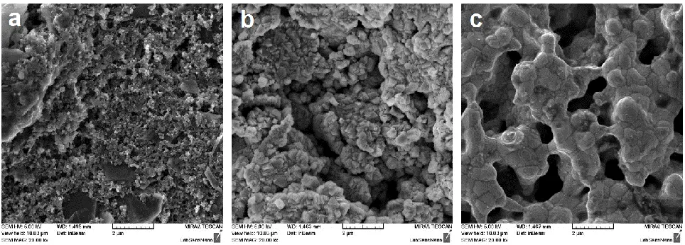
Fabricated electrodes surfaces were examined using scanning electron microscopy. All surfaces structures with magnification of 20k× are shown in Fig. 3. The WE structure is shown in Fig. 3a. It is clear that the WE surface is not covered homogenously by carbon particles, but the surface is porous and with very small crystallinity. This protruded morphology ensures that the active surface is larger than the designed geometrical area that was confirmed by measurement, where the WE area was measured and calculated using Randles-Sevcik equation for peak current as 7.54 mm2 large. It would be expected that the active area would be much higher than the designed one, but the real active area of polymer pastes is in general affected by approximately 40-70 wt% of inactive polymer filling (approx. 65% in case of BQ221 paste), which partially covers the active electrode material surface. The RE surface structure made of DuPont 5874 paste shown in Fig. 3b consists of 0.5 m big grains forming rough and crystalline morphology, thus, the active electrode area is estimated to be higher than the designed one. The AE surface structure shown in Fig. 3c made of high porous structure of melted platinum grains with diameter of about 1 m also ensures that the active electrode area is little bit larger than the designed one.
[image:7.596.49.531.525.698.2]
This was also confirmed by measurement and calculation from Randles-Sevcik equation for peak current. The measured sizes of the electrodes are shown in Table 2. It clearly follows from the results obtained that the surface of all screen-printed materials structures are in accordance with the reference structures, which means that the pastes were screen-printed properly. Based on the optical and electrical measuring of screen-printed electrodes it was clear that we obtained standard quality of printed layers without any short-circuits between the electrodes.
3.4 REs with various surfaces
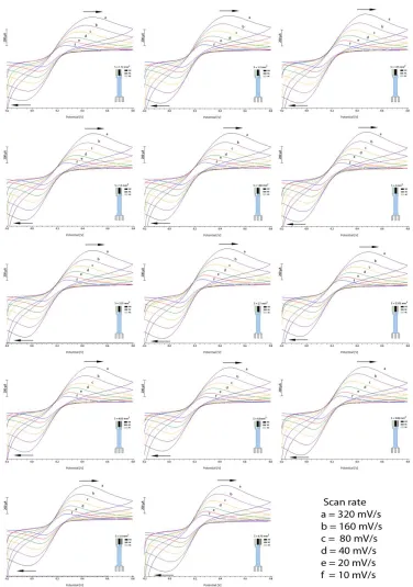
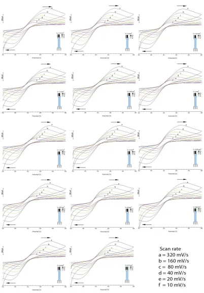
After that we characterized printed electrodes differing in areas of their RE, we tested the influence of various areas on the cathodic and anodic current responses of standard electrochemical couple of potassium ferrocyanide and ferricyanide solution measured by CV. Various scan rates as 10, 20, 40, 80, 160 and 320 mV/s were used and current responses were detected. The obtained cyclic voltammograms are shown in Fig. 4. The influence of areas of RE on both measured responses can be found in Table 3. We linearly plotted dependence of cathodic and/or anodic currents on scan rates and found equations and coefficients of determination. Based on the results it can be concluded that anodic currents were larger than cathodic, but the process was reversible due to the difference of peak potentials less than 50 mV.
Table 3. Equations and coefficients of determination for cathodic and anodic currents depending on the various surfaces of REs in measured scan rate range.
Cathodic current Anodic current
Surface [mm2]
Equation of linear plot R2 Surface [mm2]
Equation of linear plot R2
1.120 y = 698.21x + 69.028 R² = 0.9907 1.120 y = 823.43x + 57.001 R² = 0.9893 1.200 y = 691.44x + 69.029 R² = 0.9925 1.200 y = 827.69x + 58.208 R² = 0.9886 1.350 y = 667.45x + 66.747 R² = 0.9909 1.350 y = 781.60x + 58.283 R² = 0.9881 1.500 y = 668.73x + 64.592 R² = 0.9922 1.500 y = 790.40x + 56.839 R² = 0.9887 1.680 y = 673.99x + 68.258 R² = 0.9929 1.680 y = 811.98x + 57.169 R² = 0.9883 2.000 y = 668.46x + 69.870 R² = 0.9915 2.000 y = 796.80x + 56.797 R² = 0.9890 2.250 y = 682.12x + 64.098 R² = 0.9916 2.250 y = 791.18x + 54.769 R² = 0.9900 2.700 y = 648.34x + 73.185 R² = 0.9871 2.700 y = 754.65x + 60.316 R² = 0.9884 3.375 y = 666.46x + 66.509 R² = 0.9913 3.375 y = 769.95x + 57.136 R² = 0.9888 4.050 y = 699.94x + 67.542 R² = 0.9926 4.050 y = 812.66x + 58.033 R² = 0.9911 4.500 y = 705.20x + 67.319 R² = 0.9914 4.500 y = 815.64x + 56.307 R² = 0.9922 5.063 y = 742.19x + 72.327 R² = 0.9916 5.063 y = 868.11x + 60.526 R² = 0.9914 5.400 y = 726.04x + 64.765 R² = 0.9946 5.400 y = 826.09x + 60.289 R² = 0.9915 6.750 y = 722.90x + 61.685 R² = 0.9942 6.750 y = 814.03x + 58.222 R² = 0.9921
[image:8.596.27.573.447.705.2]
of anodic currents, we found that the highest responses were detected using RE with area 5.063 mm2, which well corresponds with the cathodic currents and shows stable surface and electrochemical behaviour of these electrodes in a solution. In our following experiments, we used RE with area 5.063 mm2.
[image:9.596.110.486.163.698.2]
3.5 AEs with various surfaces
[image:10.596.87.489.95.672.2]
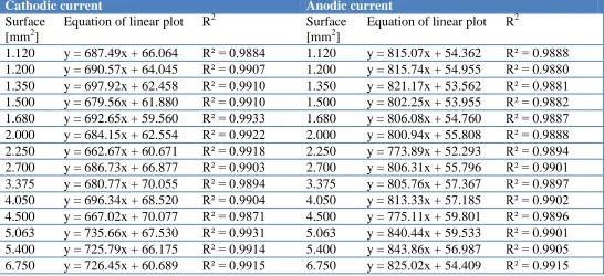
After that we optimized all of reference electrodes, which had marked influence on current response of standard electrochemical couple of potassium ferrocyanide and ferricyanide solution, we followed with the studying of the influence of various areas of auxiliary electrode (AE) on the cathodic and anodic current responses of standard electrochemical couple of potassium ferrocyanide and ferricyanide solution measured by CV. Various scan rates as 10, 20, 40, 80, 160 and 320 mV/s were again used and current responses were detected. The obtained cyclic voltammograms are shown in Fig. 5. Detected responses were measured and summarized in Table 4. We linearly plotted dependence of cathodic and/or anodic currents on scan rates and found equations and coefficients of determination. From the point of view of electrochemical process itself, we analysed well defined and reversible redox system with well-defined peaks. Considering cathodic currents only, the highest current responses expressed by the highest slopes of the dependencies obtained were found at AE with area about 5 mm2. After similar evaluation of anodic currents, we found that the highest responses were detected using RE with area 5.400 mm2 followed by area of 5.063 mm2. These results well corresponds with those obtained with various areas of REs. It is obvious that area of 5.063 mm2 seems to be very suitable for fabrication of both AE and RE, which is also very good for easy fabrication of the electrodes.
Table 4. Equations and coefficients of determination for cathodic and anodic currents depending on the various surfaces of AEs in measured scan rate range.
Cathodic current Anodic current
Surface [mm2]
Equation of linear plot R2 Surface [mm2]
Equation of linear plot R2
1.120 y = 687.49x + 66.064 R² = 0.9884 1.120 y = 815.07x + 54.362 R² = 0.9888 1.200 y = 690.57x + 64.045 R² = 0.9907 1.200 y = 815.74x + 54.955 R² = 0.9880 1.350 y = 697.92x + 62.458 R² = 0.9910 1.350 y = 821.17x + 53.562 R² = 0.9881 1.500 y = 679.56x + 61.880 R² = 0.9910 1.500 y = 802.25x + 53.955 R² = 0.9882 1.680 y = 692.65x + 59.560 R² = 0.9933 1.680 y = 806.08x + 54.760 R² = 0.9887 2.000 y = 684.15x + 62.554 R² = 0.9922 2.000 y = 800.94x + 55.808 R² = 0.9888 2.250 y = 662.67x + 60.671 R² = 0.9918 2.250 y = 773.89x + 52.293 R² = 0.9894 2.700 y = 686.73x + 66.877 R² = 0.9903 2.700 y = 806.31x + 55.796 R² = 0.9901 3.375 y = 680.77x + 70.055 R² = 0.9894 3.375 y = 805.76x + 57.367 R² = 0.9897 4.050 y = 696.34x + 68.520 R² = 0.9904 4.050 y = 813.33x + 57.185 R² = 0.9902 4.500 y = 667.02x + 70.077 R² = 0.9871 4.500 y = 775.11x + 59.801 R² = 0.9896 5.063 y = 735.66x + 67.530 R² = 0.9931 5.063 y = 840.44x + 59.533 R² = 0.9901 5.400 y = 725.79x + 66.175 R² = 0.9914 5.400 y = 843.86x + 56.987 R² = 0.9905 6.750 y = 726.45x + 60.689 R² = 0.9915 6.750 y = 825.02x + 54.409 R² = 0.9915
3.6 Testing of various RE materials
[image:11.596.26.572.415.665.2]
DuPont 5874 (AgCl), electrochemically deposited AgCl and pure Ag based TFT paste (ESL 9912-K) were tested. We independently fabricated four same electrodes and tested their behaviours. Voltammograms measured using reference electrode made of DuPont 5874 paste are shown in Fig. 6a. Voltammograms obtained were repeatable, therefore, selected material and areas of electrodes were suitable for this redox system. Similar promising results were obtained with the electrodes made of DuPont 5870 paste, as it is shown in Fig, 6b. On the other hand, the results obtained with electrochemically prepared electrodes were of worse repeatability (Fig. 6c). Pure silver based TFT REs were of poor repeatability. Based on the results obtained it can be concluded that the best behaviour was detected at electrodes made of DuPont 5874 followed by DuPont 5870 and electrochemically deposited AgCl.
[image:12.596.86.512.334.627.2]Moreover, the comparison of all measured types of reference electrodes with standard Ag/AgCl reference electrode (Theta 403, Electrochemical detectors, Turnov, Czech Republic) was done to find, whether the results are comparable with commercial standard. Cyclic voltammograms of all tested RE are shown in Fig. 6d.
Figure 6. RE output current responses to 0.05M potassium ferro-ferricyanide solution. a) DuPont 5874 commercial polymer paste. b) DuPont 5870 commercial polymer paste. c) Electrochemically coated reference electrodes. d) Tested materials comparison with standard Ag/AgCl electrode and pure silver based TFT paste.
current response is comparable. However, potentials of the measured peaks were shifted using DuPont made electrodes compared to commercial standard for more than 100 mV. The potentials measured using electrochemically fabricated reference electrodes were similar to potentials measured using DuPont polymer pastes made electrodes. It clearly follows from the results obtained that DuPont pastes are the best solution for construction of planar reference printed electrodes because of very good and reproducible response.
3.7 Testing of planarity influence to output current response
After the optimization of electrode sizes and suitability of RE materials we wondered if there will be any influence of planar system to output current response. We assumed that there could be some diffusion limitation of planar stationary system at low concentrations and high scan rates due to smaller bulk of free Fe(II) and Fe(III) ions around the planar electrodes. Therefore we compared our planar electrode system with standard-like non-planar system configuration, where just our WE from planar system was used on one side against planar AE and RE on the second side in distance of 20 mm. Comparison of both systems response to 0.5 mmol/L potassium ferro-ferricyanide solution is shown in Fig. 7. The results showed that no significant output current response change was observed for selected scan rate of 160 mV/s. It clearly follows from our results obtained that planar electrochemical systems could be also used for fast determination of low concentrations of species that are generally detected using non-planar system configuration.
Figure 7. Planar electrode system configuration output current response comparison to non-planar electrode system configuration.
4. CONCLUSIONS
[image:13.596.183.417.439.593.2]
important features of screen-printed electrodes, which should be considered before their designing, fabrication and applications for electrochemical analysis, because we found that areas as well as materials of auxiliary and reference electrode can markedly influence of current response and, therefore, markedly influence detection limit of the sensor. Finally, there was also confirmed, that these three-electrode screen-printed planar electrode systems could be used for detection of 0.5 mmol/L of ferro-ferricyanide solution at the scan rate 160 mV/s without any significant output current response change in comparison to standard-like non-planar three-electrode system predicting for presented electrodes sizes no diffusion limits impacting the low concentration determination.
ACKNOWLEDGEMENTS
Financial support from NANIMEL GACR 102/08/1546, INCHEMBIOL MSM0021622412 and CEITEC CZ.1.05/1.1.00/02.0068 is highly acknowledged. The results were presented at 11th Workshop of Physical Chemists end Electrochemists held in Brno, Czech Republic.
References
1. W. Peijnenburg, M. Zablotskaja and M. G. Vijver, Ecotox. Environ. Safe., 67 (2007) 163. 2. M. Soylak, I. Narin, U. Divrikli, S. Saracoglu, L. Elci and M. Dogan, Anal. Lett., 37 (2004) 767. 3. O. Krystofova, L. Trnkova, V. Adam, J. Zehnalek, J. Hubalek, P. Babula and R. Kizek, Sensors, 10
(2010) 5308.
4. D. Huska, V. Adam, P. Babula, L. Trnkova, J. Hubalek, J. Zehnalek, L. Havel and R. Kizek, Microchim. Acta, 173 (2011) 189.
5. D. Huska, O. Zitka, O. Krystofova, V. Adam, P. Babula, J. Zehnalek, K. Bartusek, M. Beklova, L. Havel and R. Kizek, Int. J. Electrochem. Sci., 5 (2010) 1535.
6. D. Hynek, J. Prasek, J. Pikula, V. Adam, P. Hajkova, L. Krejcova, L. Trnkova, J. Sochor, M. Pohanka, J. Hubalek, M. Beklova, R. Vrba and R. Kizek, Int. J. Electrochem. Sci., in press (2011). 7. J. Prasek, M. Adamek, J. Hubalek, V. Adam, L. Trnkova and R. Kizek, Sensors, 6 (2006) 1498. 8. V. Supalkova, M. Beklova, J. Baloun, C. Singer, B. Sures, V. Adam, D. Huska, J. Pikula, L.
Rauscherova, L. Havel, J. Zehnalek and R. Kizek, Bioelectrochemistry, 72 (2008) 59.
9. L. Trnkova, S. Krizkova, V. Adam, J. Hubalek and R. Kizek, Biosens. Bioelectron., 26 (2011) 2201.
10.O. Zitka, D. Huska, V. Adam, A. Horna, M. Beklova, Z. Svobodova and R. Kizek, Int. J. Electrochem. Sci., 5 (2010) 1082.
11.V. Adam, I. Fabrik, V. Kohoutkova, P. Babula, J. Hubalek, R. Vrba, L. Trnkova and R. Kizek, Int. J. Electrochem. Sci., 5 (2010) 429.
12.J. Petrlova, R. Mikelova, K. Stejskal, A. Kleckerova, O. Zitka, J. Petrek, L. Havel, J. Zehnalek, V. Adam, L. Trnkova and R. Kizek, J. Sep. Sci., 29 (2006) 1166.
13.D. Potesil, J. Petrlova, V. Adam, J. Vacek, B. Klejdus, J. Zehnalek, L. Trnkova, L. Havel and R. Kizek, J. Chromatogr. A, 1084 (2005) 134.
14.J. Vitecek, J. Petrlova, J. Petrek, V. Adam, D. Potesil, L. Havel, R. Mikelova, L. Trnkova and R. Kizek, Electrochim. Acta, 51 (2006) 5087.
15.O. Zitka, H. Skutkova, O. Krystofova, P. Sobrova, V. Adam, J. Zehnalek, L. Havel, M. Beklova, J. Hubalek, I. Provaznik and R. Kizek, Int. J. Electrochem. Sci., 6 (2011) 1367.
16.E. Palecek and V. Ostatna, Electroanalysis, 19 (2007) 2383.
18.J. Petrlova, D. Potesil, R. Mikelova, O. Blastik, V. Adam, L. Trnkova, F. Jelen, R. Prusa, J. Kukacka and R. Kizek, Electrochim. Acta, 51 (2006) 5112.
19.V. Adam, J. Petrlova, J. Wang, T. Eckschlager, L. Trnkova and R. Kizek, PLoS ONE, 5 (2010) e11441.
20.V. Adam, O. Zitka, P. Dolezal, L. Zeman, A. Horna, J. Hubalek, J. Sileny, S. Krizkova, L. Trnkova and R. Kizek, Sensors, 8 (2008) 464.
21.I. Fabrik, S. Krizkova, D. Huska, V. Adam, J. Hubalek, L. Trnkova, T. Eckschlager, J. Kukacka, R. Prusa and R. Kizek, Electroanalysis, 20 (2008) 1521.
22.J. Hubalek, J. Hradecky, V. Adam, O. Krystofova, D. Huska, M. Masarik, L. Trnkova, A. Horna, K. Klosova, M. Adamek, J. Zehnalek and R. Kizek, Sensors, 7 (2007) 1238.
23.D. Huska, V. Adam, O. Zitka, J. Kukacka, R. Prusa and R. Kizek, Electroanalysis, 21 (2009) 536. 24.R. Kizek, L. Trnkova and E. Palecek, Anal. Chem., 73 (2001) 4801.
25.D. Potesil, R. Mikelova, V. Adam, R. Kizek and R. Prusa, Protein J., 25 (2006) 23.
26.M. Strouhal, R. Kizek, J. Vacek, L. Trnkova and M. Nemec, Bioelectrochemistry, 60 (2003) 29. 27.L. Trnkova, R. Kizek and J. Vacek, Bioelectrochemistry, 56 (2002) 57.
28.O. Zitka, A. Horna, K. Stejskal, J. Zehnalek, V. Adam, L. Havel, L. Zeman and R. Kizek, Acta Chim. Slov., 54 (2007) 68.
29.O. Zitka, O. Krystofova, P. Sobrova, V. Adam, J. Zehnalek, M. Beklova and R. Kizek, J. Hazard. Mater., 192 (2011) 794.
30.V. Adam, D. Huska, J. Hubalek and R. Kizek, Microfluid. Nanofluid., 8 (2010) 329.
31.D. Huska, V. Adam, J. Hubalek, L. Trnkova, T. Eckschlager, M. Stiborova, I. Provaznik and R. Kizek, Chim. Oggi-Chem. Today, 28 (2010) 18.
32.D. Huska, V. Adam, S. Krizkova, J. Hrabeta, T. Eckschlager, M. Stiborova and R. Kizek, Chim. Oggi-Chem. Today, 28 (2010) 15.
33.D. Huska, V. Adam, L. Trnkova and R. Kizek, J. Magn. Magn. Mater., 321 (2009) 1474.
34.D. Huska, J. Hubalek, V. Adam, D. Vajtr, A. Horna, L. Trnkova, L. Havel and R. Kizek, Talanta, 79 (2009) 402.
35.V. Shestivska, V. Adam, J. Prasek, T. Macek, M. Mackova, L. Havel, V. Diopan, J. Zehnalek, J. Hubalek and R. Kizek, Int. J. Electrochem. Sci., 6 (2011) 2869.
36.O. Zitka, H. Skutkova, V. Adam, L. Trnkova, P. Babula, J. Hubalek, I. Provaznik and R. Kizek, Electroanalysis, 23 (2011) 1556.
37.M. Fojta, F. Jelen, L. Havran and E. Palecek, Curr. Anal. Chem., 4 (2008) 250. 38.E. Palecek, Electroanalysis, 8 (1996) 7.
39.E. Palecek, Talanta, 56 (2002) 809.
40.J. Wang, Anal. Chim. Acta, 469 (2002) 63. 41.J. Wang, Small, 1 (2005) 1036.
42.J. Wang, Electroanalysis, 17 (2005) 7.
43.S. Billova, R. Kizek, F. Jelen and P. Novotna, Anal. Bioanal. Chem., 377 (2003) 362.
44.M. Beklova, S. Krizkova, V. Supalkova, R. Mikelova, V. Adam, J. Pikula and R. Kizek, Int. J. Environ. Anal. Chem., 87 (2007) 459.
45.N. Lewen, S. Mathew, M. Schenkenberger and T. Raglione, J. Pharm. Biomed. Anal., 35 (2004) 739.
46.E. Szlyk and A. Szydlowska-Czerniak, J. Agric. Food Chem., 52 (2004) 4064. 47.O. Mikkelsen and K. H. Schroder, Electroanalysis, 15 (2003) 679.
48.I. Fabrik, J. Kukacka, J. Baloun, I. Sotornik, V. Adam, R. Prusa, D. Vajtr, P. Babula and R. Kizek, Electroanalysis, 21 (2009) 650.
49.C. Fernandez-Bobes, M. T. Fernandez-Abedul and A. Costa-Garcia, Electroanalysis, 10 (1998) 701.
51.V. Adam, J. Petrlova, D. Potesil, J. Zehnalek, B. Sures, L. Trnkova, F. Jelen and R. Kizek, Electroanalysis, 17 (2005) 1649.
52.S. Krizkova, V. Adam, J. Petrlova, O. Zitka, K. Stejskal, J. Zehnalek, B. Sures, L. Trnkova, M. Beklova and R. Kizek, Electroanalysis, 19 (2007) 331.
53.J. Petrlova, D. Potesil, J. Zehnalek, B. Sures, V. Adam, L. Trnkova and R. Kizek, Electrochim. Acta, 51 (2006) 5169.
54.V. Adam, S. Krizkova, O. Zitka, L. Trnkova, J. Petrlova, M. Beklova and R. Kizek, Electroanalysis, 19 (2007) 339.
55.V. Adam, J. Zehnalek, J. Petrlova, D. Potesil, B. Sures, L. Trnkova, F. Jelen, J. Vitecek and R. Kizek, Sensors, 5 (2005) 70.
56.K. B. Wu, S. S. Hu, J. J. Fei and W. Bai, Anal. Chim. Acta, 489 (2003) 215.
57.W. Yantasee, Y. H. Lin, G. E. Fryxell and B. J. Busche, Anal. Chim. Acta, 502 (2004) 207. 58.C. G. Hu, K. B. Wu, X. Dai and S. S. Hu, Talanta, 60 (2003) 17.
59.L. Fujcik, R. Prokop, J. Prasek, J. Hubalek and R. Vrba, Microelectron. Int., 27 (2010) 3.
60.J. Prasek and M. Adamek, in D. Rocha, P.M. Sarro, M.J. Vellekoop (Editors), Proceedings of the Ieee Sensors 2004, Vols 1-3, 2004, p. 749.
61.P. Fanjul-Bolado, D. Hernandez-Santos, P. J. Lamas-Ardisana, A. Martin-Pernia and A. Costa-Garcia, Electrochim. Acta, 53 (2008) 3635.
62.P. M. Ajayan and T. W. Ebbesen, Rep. Prog. Phys., 60 (1997) 1025. 63.K. Balasubramanian and M. Burghard, Small, 1 (2005) 180.
64.L. M. May and D. A. Russell, Anal. Chim. Acta, 500 (2003) 119.
65.J. H. Pei, M. L. Tercier-Waeber and J. Buffle, Anal. Chem., 72 (2000) 161.
66.J. Prasek, J. Drbohlavova, J. Chomoucka, J. Hubalek, O. Jasek, V. Adam and R. Kizek, J. Mater. Chem., 21 (2011) 15872.
67.J. Prasek, D. Huska, O. Jasek, L. Zajickova, L. Trnkova, V. Adam, R. Kizek and J. Hubalek, Nanoscale Res. Lett., 6 (2011) 385.
68.T. C. Reissing, Proc. Inst. Elec. Electron. Engineers, 59 (1971) 1448. 69.W. Funk, Philips Techn. Rev., 35 (1975) 144.
70.I. Palchetti, A. Cagnini, M. Mascini and A. P. F. Turner, Microchim. Acta, 131 (1999) 65. 71.R. Guell, G. Aragay, C. Fontas, E. Antico and A. Merkoci, Anal. Chim. Acta, 627 (2008) 219. 72.G. Roa, M. T. Ramirez-Silva, M. A. Romero-Romo and L. Galicia, Anal. Bioanal. Chem., 377
(2003) 763.
73.J. Cooper, J. A. Bolbot, S. Saini and S. J. Setford, Water Air Soil Pollut., 179 (2007) 183. 74.H. Palchetti, S. Laschi and M. Mascini, Anal. Chim. Acta, 530 (2005) 61.
75.R. J. Zheng, Y. M. Fang, S. F. Qin, J. Song, A. H. Wu and J. J. Sun, Sens. Actuator B-Chem., 157 (2011) 488.
76.L. Presmanes, A. Chapelle, F. Oudrhiri-Hassani, A. Barnabe and P. Tailhades, Sens. Lett., 9 (2011) 587.
77.J. Y. Jung and C. S. Lee, J. Ind. Eng. Chem., 17 (2011) 237.
78.A. Fischerauer, G. Fischerauer, G. Hagen and R. Moos, Phys. Status Solidi A-Appl. Mat., 208 (2011) 404.
79.V. Manickam, E. Prabhu, V. Jayaraman, K. I. Gnanasekar, T. Gnanasekaran and K. S. Nagaraja, Measurement, 43 (2010) 1636.
80.S. Reiss, G. Hagen and R. Moos, Sensors, 8 (2008) 7904.
81.M. C. Chuang, Y. L. Yang, T. F. Tseng, T. Chou, S. L. Lou and J. Wang, Talanta, 81 (2010) 15. 82.M. Piano, S. Serban, N. Biddle, R. Pittson, G. A. Drago and J. P. Hart, Anal. Biochem., 396 (2010)
269.
84.H. B. Li, J. Li, Z. J. Yang, Q. Xu, C. T. Hou, J. Y. Peng and X. Y. Hu, J. Hazard. Mater., 191 (2011) 26.
85.G. Aragay, J. Pons and A. Merkoci, J. Mater. Chem., 21 (2011) 4326.
86.O. Zaouak, L. Authier, C. Cugnet, A. Castetbon and M. Potin-Gautier, Electroanalysis, 22 (2010) 1151.
87.A. Mandil, L. Idrissi and A. Amine, Microchim. Acta, 170 (2010) 299. 88.K. C. Honeychurch, S. Al-Berezanchi and J. P. Hart, Talanta, 84 (2011) 717.
89.G. H. Hwang, W. K. Han, J. S. Park and S. G. Kang, Sens. Actuator B-Chem., 135 (2008) 309. 90.E. Khaled, H. N. A. Hassan, I. H. I. Habib and R. Metelka, Int. J. Electrochem. Sci., 5 (2010) 158. 91.M. H. Chiu, A. S. Kumar, S. Sornambikai, P. Y. Chen, Y. Shih and J. M. Zen, Int. J. Electrochem.
Sci., 6 (2011) 2352.
92.Y. H. Won, K. Huh and L. A. Stanciu, Biosens. Bioelectron., 26 (2011) 4514.
93.M. Moreno, V. M. Gonzalez, E. Rincon, A. Domingo and E. Dominguez, Analyst, 136 (2011) 1810.
94.J. Galandova, R. Ovadekova, A. Ferancova and J. Labuda, Anal. Bioanal. Chem., 394 (2009) 855. 95.G. Ziyatdinova, J. Galandova and J. Labuda, Int. J. Electrochem. Sci., 3 (2008) 223.
96.J. F. Ping, S. P. Ru, X. Luo, K. Fan, J. Wu and Y. B. Ying, Electrochim. Acta, 56 (2011) 4154. 97.L. H. J. Xiong, C. Batchelor-McAuley, L. M. Goncalves, J. A. Rodrigues and R. G. Compton,
Biosens. Bioelectron., 26 (2011) 4198.
98.O. A. Loaiza, E. Jubete, E. Ochoteco, G. Cabanero, H. Grande and J. Rodriguez, Biosens. Bioelectron., 26 (2011) 2194.
99.J. Kumar and S. F. D'Souza, Biosens. Bioelectron., 26 (2011) 4289. 100. I. E. Mulazimoglu, Energy Educ. Sci. Technol.-Part A, 28 (2011) 393.
101. E. Y. Z. Frag, G. G. Mohamed and H. M. S. Alelaiwi, J. Electroanal. Chem., 659 (2011) 121. 102. M. Liu, J. J. Hu, T. Ma, S. Wang and H. Ding, Anal. Sci., 27 (2011) 839.
103. S. H. Zhen, Y. Wang, C. G. Liu, G. M. Xie, C. S. Zou, J. Zheng and Y. Zhu, Forensic Sci. Int., 207 (2011) 177.
104. T. Garcia, M. G. Fernandez-Barrena, M. Revenga-Parra, A. Nunez, E. Casero, F. Pariente, J. Prieto and E. Lorenzo, Anal. Bioanal. Chem., 398 (2010) 1385.
105. P. Rai, P. S. Kumar, S. Oh, H. Kwon, G. N. Mathur and V. K. Varadan, in V.K. Varadan (Editor), Nanosensors, Biosensors, and Info-Tech Sensors and Systems 2011, Spie-Int Soc Optical Engineering, Bellingham, 2011.
106. M. Lanz, D. Schurch and G. Calzaferri, J. Photochem. Photobiol. A-Chem., 120 (1999) 105