Abstract: A wireless sensor network is an accumulation of
sensor nodes in large quantities with limited energy resources. Thus, use of energy efficient power amplifiers is an essential requirement for sensor nodes as power amplifiers are responsible for the main power consumption in the transceivers of sensor nodes. The transceivers should operate at high data rate for better efficiency which allows many nodes to share same channel through time division multiplexing. Thus, wider band width is another important requirement for power amplifiers used in sensor transceivers. Reliability of a power amplifier can be increased by designing at smaller supply voltage.
This paper suggests improvements in design of power amplifier in class E configuration, for transceivers in wireless sensor nodes. In order to achieve wider band width, cascade of common drain followed by common source in class E configuration has been designed; and for more reliable operation with higher efficiency, class E in double cascoded has been implemented. The proposed designs are simulated in SPICE and higher efficiencies and band widths are achieved.
Index Terms: Class E power amplifier, Double cascoding; Low
power transceivers, Power MOSFET, Switch mode power amplifier.
I. INTRODUCTION
Current developments in computers, telecommunication and microelectronics have simplified the design of small size, multifunctional sensor nodes with low-power and low cost in large quantity. They can sense various information from the surroundings, like humidity, seismic vibrations, light, temperature, nature of biological organisms etc. Being very small in size, these nodes have embedded processing abilities. These nodes can have multiple sensors operating in infra-red (IR), seismic, acoustic and magnetic modes. A sensor network consists of densely deployed sensor nodes in a region to monitor a particular phenomenon. Sensor network is a fresh research area with applications in military surveillance, environmental/habitat monitoring, inventory tracking, medical monitoring, disaster management, traffic management and monitoring, smart home and more. Sensors are used to measure or monitor parameters that differ with time and location necessitating the need for the Dynamic
Revised Manuscript Received on May 10, 2019.
Saji. M. Antony, Research Scholar, ECE Department, Delhi Technological University, New Delhi.
Assistant Professor, ECE Department, Bharati Vidyapeeth’s College of Engineering, New Delhi.
Dr. S. Indu, Professor, ECE Department, Delhi Technological University, New Delhi.
Dr. Rajeshwari Pandey, Professor, ECE Department, Delhi Technological University, New Delhi.
Sensor Networks (DSN) [1]. Fig. 1 Shows Components of a Sensor Node.
[image:1.595.318.548.231.355.2]
Fig. 1. Components of Sensor Node [2]
Life of a sensor network mainly depends on its energy consumption. Commercially available sensor nodes are battery driven devices. Due to plenty of sensor nodes installed in an isolated area and long lifespan requirement, replacing battery is not an option. So, energy optimization in sensor network is more complicated as it involves reducing the energy utilization and increasing the lifespan of sensor network.
In sensor nodes, power is consumed mainly in transceivers [3] and in transceivers, the most significant power consumption is attributed to power amplifiers [4]. This paper focuses on design of switch mode power amplifiers in class E configuration with high power efficiency. In [5], N O Sokal has introduced class‑ E amplifier with parallel capacitor and obtained ideal power efficiency value as 100%.
II. RELATEDWORK
Due to the demand of low power sensor nodes in wide range of applications, recent research has been focussed on every block of sensor nodes. I F Akyildiz et. al focuses on the importance of power conservation and power management in sensor networks [3]. Being low in cost, sensor nodes are deployed, in hundreds and thousands, for tasks ranging from battlefield surveillance to environmental sampling. It is important to save battery power on these micro-electronic device, due to the inaccessible regions where sensor networks are mostly deployed. In most of the applications, renewing power resources may not be possible. So life time of sensors greatly relies upon lifespan of battery. In [6], W Dargie focuses on selective switching and voltage scaling. To achieve low power and long
life time, circuit-level design procedures are focused in [7]. Importance of low power
Design Improvements in Power Amplifier
for Making Energy Efficient Transceiver Blocks
of Sensor Nodes
transceiver design is explained in [8]. This paper focuses on the design parameters which significantly influence energy consumption of transceiver unit. D G Rahn et.al have designed a transceiver for multiple input/multiple output wireless LAN applications in [9]. In RF transceivers, the major power consumption unit is power amplifier. Class AB operation is suitable for improved linearity and higher power added efficiency. Adaptive biasing schemes can be implemented for low power applications. Low power amplifier with adaptive biasing is designed in reference [10].
High linearity, greater average output power, wider operating bandwidths and reduced energy consumption are the key design aspects for power amplifiers. When power amplifiers working in switch-mode configuration, the transistor operates in saturation, and either voltage or current, is switched on and off, depending on class of amplifier. A switch can be used in place of transistor. Only voltage is present across an open switch and current flows through the closed switch. So class E power amplifier has zero overlap of time between voltage and current. It gives 100% theoretical efficiency. Class-E power amplifier is a compromise between switched configuration and linear class AB configuration [11, 12]. Reference [13] presents a two stage class E linear power amplifier with greater power added efficiency.
In order to achieve higher degree of gain, the cascode amplifier configuration can be used. For collecting neural data from implanted electrodes, an RFID reader with high resolution is proposed in [4]. In reference [14], S. Du et.al described single ended power amplifier for WLAN applications. Higher gain and better efficiency can be achieved with current reused technique in driver stage and self-biased technique in power stage. Design of self-biased class E amplifier is given in [15].
III. PROBLEMFORMULATION
The efficiency and bandwidth are the most important characteristics of power amplifier in sensor nodes. Low power sensor nodes must communicate with their neighbours at hundreds of kilobytes per second and have to operate at higher volumetric densities. High data rate requires wider band width. But wider bandwidth limits the sensitivity and range. Requirement of wider bandwidth and higher efficiency without reducing sensitivity demands new design strategies.
Power amplifier with low power supply gives more reliable operation. But overall gain and efficiency are decreased due to reduced power supply.
In class E power amplifiers, these combinations do not exist. So we are proposing modifications for basic class E amplifier to achieve improved band width and efficiency at lower power supply.
IV. POWERAMPLIFIER
Power amplifiers are mainly responsible for power consumption in transceivers. So recent research focussed on
power amplifiers in switch mode configuration [8,16]. The RF power amplifiers are classified as classes A-F depending on method of operation. An RF power amplifier uses an active device (BJTS, JFETS, MOSFETS, GaAs MESFETS etc.), dc feed and output matching network.
V. CLASSEPOWERAMPLIFIER
The research in switch mode configuration of power amplifier aims to increase efficiency and band width without reducing linearity. Class E designs are commonly used due to greater power efficiency. An amplifier in class E design is shown in Fig 2 [17]. It is designed with transistor Q as switch, a shunt capacitor Cp, and a series LC circuit. The LF is a radio
frequency choke, which has high impedance at operating frequency. The values of Cp, L, C, LF and RL are selected
such that power switching losses of transistor are minimized. The shunt capacitor absorbs the parasitic capacitance at the output of transistor. Presence of larger shunt capacitor for same power, load and supply, enables to operate at high frequencies. When transistor is off, current bypasses through the shunt capacitor. LC series resonator circuit allows current of fundamental frequency to flow from output to load. Finite dc inductance gives efficient output matching network. It also provides many other benefits like reduction in size, supply voltage and cost.
[image:2.595.315.544.448.569.2]For Class E amplifier output waveforms are analog in shape compared with the ideal pulse shaped form of other modes of operation. So class E amplifiers can be supported by slow switching transistors and are better suited to high frequency operation. Class E power amplifier with shunt capacitor gives 100% ideal power efficiency [9].
Fig 2. Class E power amplifier [19]
The design equations [14, 19-23] for class E power amplifier are as below:
The load resistance RL is given by
(1)
where VCC andP represent dcsupply voltage and power
respectively.
The current drawn from dc supply (Io) can be expressed as
The shunt capacitance may be computed as:
(3)
The components L and C of series resonator are respectively given by (4) and (5). (4)
(5) The radio frequency choke inductance may be computed as (6)
Input power (7)
Output power: (8)
Efficiency: (9)
VI. PROPOSEDDESIGN
To make class E amplifier suitable for sensor nodes, two different configurations using basic class E amplifier are proposed in this work. The first configuration is class E amplifier with double cascoding and second design is class E amplifier designed using common drain followed by common source (CDCS) cascading. These configurations are discussed in the following subsections.
A. The Cascode Amplifier
A cascade of common source amplifier followed by common gate is termed as cascode amplifier. The basic idea behind cascode amplifier is to combine the high frequency response and current buffering properties of common gate configuration high input resistance and with large trans- conductance obtained in common source amplifier. Absence of Miller effect makes common gate high frequency response far superior to common source configuration [18].
The Cascode topology allows design of power amplifier at reduced VG and VDS, which leads to more reliable operation
[19]. Higher output resistance and higher gain can be obtained by adding another level of cascoding. Here another transistor in common gate is added, and it results higher output resistance increased by a factor equal to voltage gain. Common gate configuration acts as current buffer. It takes input signal current at low input resistance and provides nearly equal current at very high output resistance. Presence of common gate configuration has resulted in increased load current thus increased efficiency and bandwidth [18].
B. Common Drain Common Source (CD-CS) Configuration.
Common drain common source cascading gives wider band width, compared with common source configuration. Transistor in common source configuration, will exhibit a Miller effect that results in large input capacitance. Buffering action of common drain configuration causes a low resistance across input capacitance of common source configuration.
Impedance match provided by the common drain configuration in CD-CS cascading results less loss across the load. It leads high load current and increases efficiency and bandwidth [18].
VII SIMULATIONRESULTS
The performance of designed configurations is proved with PSPICE simulation. First, Class E amplifier with double cascoding as shown in Fig. 3(a) is simulated. Following design specifications are used for double cascode class E amplifier: Supply voltage = 12V, Output power = 10W, D = 0.5, Q= 10. For given specifications components values are computed as RL = 8.31Ω, LF = 57.6 µH, LS= 13.22 µH, CS
= 2.17nF. The RD for CS configuration is considered as 30 Ω
and RS for CG configuration is 100 Ω. Power MOSFET IRF
510 is used for simulation purpose. Transient output of double cascode class E amplifier is as shown in Fig. 3(b). Load current measured is IRL (RMS) = 1.71 Amp , with DC
current IDC = 2.1Amp. The efficiency for the observed values
is computed as 96.43%.
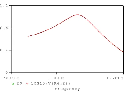
Frequency response of double cascode class E amplifier is as shown in Fig. 3(c). Band width for this configuration is obtained as 284.4 KHz.
The CD-CS configuration is implemented as shown in Fig. 4(a). switching transistor IRF 510 is used for both CD and CS configuration. Supply voltage = 12V, 1MHz square pulse of amplitude 1V is applied as VG. This configuration is also
simulated for same design specifications as used for double cascoding amplifier. For given specifications components values are computed using design equations as RL = 8.31Ω,
LF = 57.6 µH, LS= 13.22 µH, CS = 2.17nF. The value of RD
for CS configuration is chosen to be 30 Ω and the RS for CD
configuration is considered to be 100 Ω.
Transient output of class E CD-CS configuration is shown in Fig. 4(b). The rms value of load current IRL (RMS) is obtained
as 4.39 Amp and the dc current is observed to be IDC 14.1
Amp. Hence, the efficiency is computed as 94.65%.
Frequency response of CDCS class E configuration is as shown in Fig. 4(c) and the band width obtained is 391 KHz.
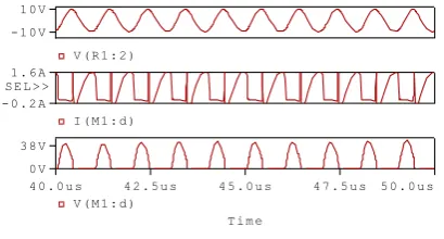
The existing class E circuit shown in Fig. 5(a) is also simulated for same simulation settings to compare the performance of proposed designs. The transient output is showed in Fig. 5(b) where the peak switch voltage is obtained as 43.8V and current is observed as 1.65 Amps. From these simulated values the
It is thus observed that proposed designs outperform in terms of efficiency and bandwidth. The results are summarised in Table 1. It is found from the table that the proposed class E double cascoded configuration is suitable for wide band width and increased efficiency. The CD-CS Class E amplifier gives Maximum bandwidth.
Fig 3(a): Class E amplifier with double cascoding.
Fig 3(b): simulation results of class E amplifier with double cascoding.
F r e q u e n c y 1 . 0 M H z
7 0 0 K H z 1 . 7 M H z
2 0 L O G 1 0 ( V ( R 4 : 2 ) ) 0
0 . 4 0 . 8 1 . 2
Fig 3(c): Frequency response of double cascode amplifier
Fig 4(a): class E amplifier with CD-CS cascading
T i m e
4 0 . 0 u s 4 2 . 5 u s 4 5 . 0 u s 4 7 . 5 u s 5 0 . 0 u s
V ( R 2 : 1 ) 0 V
5 0 V
I D ( M 2 ) 0 A
7 . 5 A
V ( R 3 : 2 ) - 1 0 V
S E L > >
Fig. 4(b): simulation results of class E amplifier with CD-CS cascading.
Fig 4(c): Frequency response of CD-CS cascading
[image:4.595.325.527.62.194.2] [image:4.595.62.278.134.255.2] [image:4.595.331.530.239.345.2] [image:4.595.70.276.299.438.2] [image:4.595.327.528.404.556.2] [image:4.595.73.272.480.625.2] [image:4.595.325.522.611.714.2]Author-1 Photo
T i m e
4 0 . 0 u s 4 2 . 5 u s 4 5 . 0 u s 4 7 . 5 u s 5 0 . 0 u s V ( M 1 : d )
0 V 3 8 V
I ( M 1 : d ) - 0 . 2 A
1 . 6 A S E L > >
V ( R 1 : 2 ) - 1 0 V
1 0 V
Fig. 5(b): Simulation results of simple class E amplifier circuit.
F r e q u e n c y 1 . 0 M H z
6 0 0 K H z 1 . 8 M H z
2 0 L O G 1 0 ( V ( R 1 : 2 ) ) 0
0 . 5 1 . 0 1 . 5
[image:5.595.71.276.63.173.2]Fig 5(c): Frequency response of class E amplifier
TABLE 1.
PERFORMANCE COMPARISON TABLE
Circuit DC Current
(IDC)
RMS
current
( IRL)
Efficiency Band Width
Simple Class E Amplifier
0.52A 0.83A 91.67% 97.3KHz
Proposed double Cascode Class E
amplifier
2.1A 1.71A 96.43% 284.4KHz
Proposed CD-CS Class
E amplifier 14.1A 4.39A 94.65% 391KHz
VII. CONCLUSION
Design of power amplifiers for sensor nodes requires extensive research to meet requirements for linearity, efficiency, output power, band width. Class E power amplifiers are designed and simulated with double cascoding and CD-CS cascading. Simulated results show better efficiency and band width as compared to existing class E amplifier.
Further low power and high accuracy can be achieved using optimal pulse bias. To reduce supply voltage and DC power consumption, Darlington configuration can be employed. To improve the efficiency, self-bias can be implemented in double cascoding and CD-CS configurations.
REFERENCES
1. Anil Kumar, Preeti Gulia, Shikha Sharma, “A Study on Power Saving and Secure WSN”, International Journal of Engineering Trends and Technology (IJETT), Volume 11 Number 4, May 2014.
2. Saji M Antony, Dr S Indu, Dr Rajeshwari Pandey, “Design of High speed Low Power Multiplier for Sensor Nodes”, International Journal of control Theory and Applications, Vol 11,2018.
3. I. F. Akyildiz, W. Su, Y. Sankarasubramaniam, E. Cayirci. “Wireless sensor networks: a survey”, Computer Networks, 38, 2002 pp. 393-422 4. Daniela DeVenutoa, N, JanRabaey B, “RFID transceiver for wireless powering brain implanted microelectrodes and backscattered neural data collection”, Microelectronics Journal45, 2014, pp 1585–1594. 5. Nathan O. Sokal, Alan D. Sokal, “Class E - A New Single-Ended Class
of High-Efficiency Tuned Switching Power Amplifiers”, IEEE Journal of Solid-State Circuits, Vol. Sc-10, No. 3, June 1975.
6. Waltenegus Dargie, “Dynamic Power Management in Wireless Sensor Networks: State-of-the-Art”, IEEE Sensors Journal, Vol. 12, No. 5, May 2012.
7. Mark Hempstead, Nikhil Tripathi, Patrick Mauro, Gu-Yeon Wei, David Brooks, “An Ultra-Low Power System Architecture for Sensor Network Applications”, Proceedings of the 32nd International Symposium on Computer Architecture (ISCA’05) IEEE , 2005, pp. 1063-6897. 8. Adinya John Odey, Daoliang Li, “Low Power Transceiver Design
Parameters for Wireless Sensor Networks. Wireless Sensor Network, 4, 2012, pp. 243-249.
9. David G. Rahn, Mark S. Cavin, Fa Foster Dai, Neric H. W. Fong, Richard Griffith, José Macedo, A. David Moore, John W. M. Rogers, and Mike Toner, “A Fully Integrated Multiband MIMO WLAN Transceiver RFIC”, IEEE Journal of Solid-State Circuits, Vol. 40, No. 8, August 2005.
10.Sangsu Jin, Byungjoon Park, Kyunghoon Moon, Myeongju Kwon and Bumman Kim, “Linearization of CMOS Cascode Power Amplifiers Through Adaptive Bias Control”, IEEE Transactions on Microwave Theory and Techniques, Vol. 61, No. 12, 2013, pp. 4534 – 4543 11.Y. H. Chee, J. Rabaey, A. M. Niknejad, “A Class A/B Low Power
Amplifier for Wireless Sensor Networks”,ISCAS, 2004.
12.Bo Berglund, Jan Johansson and Thomas Lejon, “High efficiency power amplifiers”, Ericsson 92, Review No. 3, 2006.
13.MousaYousef, Ziaadin Daie Koozehkanani, JafarSobhi, Hamid Jangi “A 1.8 GHz Power Amplifier Class-E with Good Average Power Added Efficiency”, Circuits and Systems,2013,4, pp. 504-509.
14.SichunDua, WenbinHuanga, ChunhuaWanga, HongxiaYina and ZhiwenLianga, A College of Information Science and Engineering, Hunan University, Changsha 410082, “A Single-chip Highly Efficient CMOS Class-E Power Amplifier for WLAN Applications”, IETE Journal of Research, 01 Sep 2014
15.TirdadSowlati, Domine M. W. Leenaerts, A 2.4-GHz 0.18-m CMOS Self-Biased Cascode Power Amplifier, IEEE Journal of Solid-State Circuits, Vol. 38, No. 8, August 2003.
16.More Prachi Gopalrao, A. A. Yadav. “A Survey on RF Power Amplifier Designing with CMOS Technology”, International Journal of Computer Applications, 2016, pp. 0975 – 8887.
17.Y. Yusmarnita, Shakir Saat, A. H. Hamidon, Huzaimah Husin, Norezmi Jamal, Kamarudin. Kh, Imran Hindustan, “Design and Analysis of 1MHz Class-E Power Amplifier”, WSEAS Transactions on Circuits and Systems, Volume 14, 2015.
18.A S Sedra, K C Smith, “Microelectronic Circuits Theory and Applications”, Oxford publication, Fifth Edition.
19.Daniela DeVenuto, JanRabaey, “RFID transceiver for wireless powering brain implanted microelectrodes and backscattered neural data collection”, Microelectronics Journal-45, 2014, pp. 1585–1594.
AUTHORSPROFILE
Ms Saji M Antony is a research scholarpursuing PhD from Delhi Technological University(DTU), New Delhi. Her areas of research interest include Analog Electronics and Wireless Sensor Networks. She received her B Tech and M Tech Degrees in Electronics & Communication Engineering(ECE). She has also acquired an MSc Degree in Computer Science from Bhundelkhand University scuring first rank. She joined as a lecturer in the Dept of ECE,
[image:5.595.72.273.237.357.2] [image:5.595.51.292.422.602.2]Dr Indu S is aprofessor and head of the Department of ECE, Delhi Technological University, New Delhi. She has vast experience as a teacher and guide in research projects. She has published a book “Smart Camera Networks” and has authored a chapter of the book “Video Surveillance” published by INTECH, UK.She has published around 70 papers in national and international journals and conferences. She has completed three prestigious projects as Principal Investigator, sponsored by Naval Research Board and Department of Science and Technology, Govt of India.
![Fig. 1. Components of Sensor Node [2] Life of a sensor network mainly depends on its energy](https://thumb-us.123doks.com/thumbv2/123dok_us/8203659.261589/1.595.318.548.231.355/components-sensor-node-sensor-network-mainly-depends-energy.webp)
![Fig 2. Class E power amplifier [19]](https://thumb-us.123doks.com/thumbv2/123dok_us/8203659.261589/2.595.315.544.448.569/fig-class-e-power-amplifier.webp)