University of Southern Queensland
Faculty of Health, Engineering & Sciences
Controller Area Network to Modbus Network Bridge to
interface gas detection units with Building Management
Systems
A dissertation submitted by
Matthew Quinton
in fulfilment of the requirements of
ENG4112 Research Project
towards the degree of
Bachelor of Electrical & Electronic Engineering
Abstract
Building Management Systems (BMS') are computer systems designed to control systems
inside buildings or other facilities. While BMS' are common, there is no one size fits all
approach. Controller Area Network (CAN) is a communication protocol sometimes used within BMS'. Modbus is a very common industrial communications protocol. The two
protocols are not directly compatible and need to be ’bridged’ to communicate with each other.
Gas Detection Australia (GDA) design and manufacture gas detection equipment. They have a current and ongoing need to interface Modbus enabled equipment with CAN enabled equipment in client BMS'. This project is sponsored with the aim of producing
a network bridge to translate between the two protocols. The specific Modbus variation implemented is Modbus ASCII master.
The design was based around the PIC 18F87K22 microprocessor. This was chosen to remain consistent with other GDA products. The communication interfaces were designed using integrated circuits that closely mimic the software development tools. This was a deliberate choice made to make software development simpler and to make it easier to translate source code to the finished product. A testing method was also created to allow the assessment of bridge performance.
University of Southern Queensland Faculty of Health, Engineering & Sciences
ENG4111/2 Research Project
Limitations of Use
The Council of the University of Southern Queensland, its Faculty of Health, Engineering & Sciences, and the staff of the University of Southern Queensland, do not accept any responsibility for the truth, accuracy or completeness of material contained within or associated with this dissertation.
Persons using all or any part of this material do so at their own risk, and not at the risk of the Council of the University of Southern Queensland, its Faculty of Health, Engineering & Sciences or the staff of the University of Southern Queensland.
This dissertation reports an educational exercise and has no purpose or validity beyond this exercise. The sole purpose of the course pair entitled “Research Project” is to con-tribute to the overall education within the student’s chosen degree program. This doc-ument, the associated hardware, software, drawings, and other material set out in the associated appendices should not be used for any other purpose: if they are so used, it is entirely at the risk of the user.
Dean
Certification of Dissertation
I certify that the ideas, designs and experimental work, results, analyses and conclusions set out in this dissertation are entirely my own effort, except where otherwise indicated and acknowledged.
I further certify that the work is original and has not been previously submitted for assessment in any other course or institution, except where specifically stated.
Matthew Quinton
Acknowledgments
I would like to thank my academic supervisor, Mr Mark Phythian for his guidance and support. He often went above and beyond to help me achieve my project aims.
I would also like to thank my two professional supervisors from Gas Detection Australia, Mr James Boucher and Mr Chris Kelly. Without any of these people this project could not have taken place. I would especially like to recognise Mr Kelly, who was a continuous source of knowledge throughout the project. I would also like to thank Mr Trent Rutten from GDA for his assistance with hands on technical matters.
Finally I would like to thank my wife, Sam who was always there to listen and to help me through this project. Her patience and understanding were vital.
Contents
Abstract i
Acknowledgments iv
List of Figures xii
List of Tables xiv
Chapter 1 Introduction 1
1.1 Motivation . . . 2
1.2 Aim . . . 2
1.3 Project Objectives . . . 3
1.4 Overview of the Dissertation . . . 4
Chapter 2 Relevant Literature and Design Constraints 5 2.1 Chapter Overview . . . 6
2.2 Building Management Systems . . . 7
2.3 Controller Area Network . . . 8
CONTENTS vi
2.3.2 Standards . . . 9
2.3.3 Frame Format . . . 9
2.4 Modbus . . . 11
2.4.1 General Modbus Features . . . 11
2.4.2 Frame Format . . . 13
2.4.3 RTU, ASCII and TCP . . . 14
2.5 Bridging the Protocols . . . 15
2.5.1 Previous Works . . . 15
2.5.2 Lessons from Previous Works . . . 16
2.5.3 Existing Bridges and Available Products . . . 17
2.6 Constraints . . . 20
2.7 Chapter Summary . . . 20
Chapter 3 Design Methodology 21 3.1 Chapter Overview . . . 22
3.2 Equipment . . . 23
3.3 Hardware Design . . . 24
3.3.1 Microprocessor . . . 24
3.3.2 CAN Interface . . . 25
3.3.3 Serial Interface . . . 26
3.3.4 Power Supply . . . 26
CONTENTS vii
3.3.6 Ancillary Circuitry . . . 27
3.3.7 Printed Circtuit Board . . . 29
3.4 Software Design . . . 30
3.4.1 CAN Interface . . . 30
3.4.2 Modbus Interface . . . 30
3.4.3 Ancillary Functions . . . 31
3.4.4 Main . . . 32
3.5 Proposed Testing Methodology . . . 33
3.5.1 RS485 Confirmation . . . 34
3.5.2 Physical Cable Testing . . . 34
3.6 Chapter Summary . . . 35
Chapter 4 Design of the Network Bridge 36 4.1 Chapter Overview . . . 37
4.2 Hardware Design . . . 38
4.2.1 Microprocessor . . . 38
4.2.2 CAN Interface . . . 38
4.2.3 Serial Interface . . . 39
4.2.4 Power Supply . . . 40
4.2.5 Isolation . . . 41
4.2.6 Ancillary Circuitry . . . 41
CONTENTS viii
4.3 Software Design . . . 44
4.4 Chapter Summary . . . 47
Chapter 5 Results and Discussion 48 5.1 Results . . . 49
5.1.1 Proof of bridge concept . . . 49
5.1.2 Bridge stress testing . . . 51
5.1.3 Proof of RS-485 concept . . . 53
5.1.4 Physical Cable Testing . . . 54
5.2 Discussion . . . 57
5.2.1 Proof of Concept . . . 57
5.2.2 Stress Tests . . . 57
5.2.3 Proof RS-485 Concept . . . 58
5.2.4 Physical Cable Testing . . . 58
5.2.5 Discussion of issues and limitations - CAN Interface . . . 59
5.2.6 Discussion of issues and limitations - Modbusslave simulator . . . 62
5.3 Chapter Summary . . . 63
Chapter 6 Conclusion and Future Work 64 6.1 Conclusions . . . 65
6.2 Recommendations and Future Work . . . 66
CONTENTS ix
Appendix A Project Specification 71
Appendix B Controller Area Network 74
B.1 List of frame field descriptions . . . 75
B.2 Physical Connection . . . 76
B.2.1 Topology . . . 76
B.2.2 Transmission and Signals . . . 76
B.2.3 Encoding . . . 78
B.2.4 Synchronisation and Bit Stuffing . . . 79
B.2.5 Errors . . . 80
B.3 Masks and Filters . . . 81
Appendix C Modbus 82 C.1 Protocol Data Unit . . . 83
C.2 Error Checking . . . 83
C.3 Physical Media . . . 83
C.4 RS 485 Data Rates . . . 84
C.5 Encoding and Synchronisation . . . 84
Appendix D Network Bridge Source Code - C 85 D.1 C Header . . . 86
D.2 Modbus Functions . . . 87
CONTENTS x
D.4 Main Function . . . 94
Appendix E Hardware Design Images 97 E.1 Schematic . . . 98
E.2 PCB Top Layer . . . 99
E.3 PCB Bottom Layer . . . 100
E.4 PCB 3D Top Layer . . . 101
E.5 PCB 3D Bottom Layer . . . 102
Appendix F Results and Discussion Supporting Information 103 F.1 Click Board Schematics . . . 104
F.2 Photos . . . 106
F.3 Code Listings . . . 107
Appendix G Datasheets 108 G.1 PIC18F87K22 . . . 109
G.2 DF04S . . . 113
G.3 HCPL-2601.S . . . 115
G.4 LM2671 . . . 118
G.5 MCP2515 . . . 120
G.6 MCP2551 . . . 126
G.7 ROE0505S . . . 127
CONTENTS xi
H.1 Overview . . . 129
H.2 Technical Manual . . . 129
H.3 Operators Manual . . . 130
H.4 Software Manual . . . 130
List of Figures
2.1 CAN Frame - 11bit Identifier (adapted from (Corrigan 2008a)). . . 10
2.2 CAN Frame - 11bit Identifier (adapted from (Corrigan 2008a)). . . 10
2.3 Modbus RTU Frame (adapted from (Thomas 2008)). . . 13
2.4 Modbus ASCII Frame (adapted from (Thomas 2008)). . . 13
4.1 Network Bridge Logical Overview . . . 37
4.2 CAN Communications Hardware Interface . . . 39
4.3 Serial Communications Hardware Interface . . . 39
4.4 Power Supply Hardware . . . 40
4.5 Indication LEDs . . . 41
4.6 Bridge Data Flow Diagram . . . 44
5.1 Proof of bridge concept - complete transmission . . . 50
5.2 Percentage of frames received . . . 52
5.3 RS-485 master packet using 3.3V click board . . . 53
5.4 Short transmission line CAN traffic . . . 54
LIST OF FIGURES xiii
5.6 10 meter twisted pair CAN traffic . . . 55
5.7 10 meter twisted pair CAN traffic on working bus . . . 56
5.8 10 meter twisted pair CAN response . . . 56
5.9 Code exert of serial data sent . . . 62
5.10 Serial synchronisation errors with 16MHz crystal . . . 62
B.1 CAN bit levels (adapted from (ISO 2003a)). . . 77
B.2 NRZ and Manchester Encoding (adapted from (CAN in Automation 2015a)). 78 B.3 CAN bit stuffing (adapted from (CAN in Automation 2015a)). . . 79
F.1 RS-485 Click board schematic . . . 104
F.2 CANSpi Click board schematic . . . 105
List of Tables
2.1 Modbus memory organisation . . . 12
Glossary of Terms
A - Ampere
AC - Alternating Current
ASCII - American Standard Code for Information Exchange CAN - Controller Area Network
CR - Carriage Return (ASCII character) DC - Direct Current
DFD - Data Flow Diagram
GDA - Gas Detection Australia Pty Ltd GLCD - Graphical Liquid Crystal Display IC - Integrated Circuit
IP - Ingress Protection Rating LED - Light Emitting Diode LF - Line Feed (ASCII Character) OSI - Open Systems Interconnection PCB - Printed Circuit Board
RMS - Root Mean Squared SPI - Serial Peripheral Interface
UART - Universal Asynchronous Receiver/Transmitter USB - Universal Serial Bus
V - Voltage/Volts
Chapter 1
1.1 Motivation 2
1.1
Motivation
GDA designs and manufactures electronic gas sensors and control units. Most of the sensors are industry standard 4-20 mA output and are hard wired back to control units. These control units are restricted by only having Modbus, relay switched Volt Free Con-tacts (VFC) and analogue current outputs to communicate with the customers' existing
equipment. There are a growing number of customers requesting or already using Con-trolled Area Network (CAN) bus as part of their Building Management System (BMS), which GDA doesn't currently or plan to support as a direct hardware feature in their
pre-existing products.
GDA wants to explore the development of a CAN bus to Modbus network bridge to allow customers to directly interface their BMS with GDA control units to simplify the installation and increase customer satisfaction. The current methods are to add a 4-20 mA current receiver and a CAN bus node with analogue inputs or a CAN bus node with digital inputs to receive the digital signals generated by the output relays on the control units. Depending upon the complexity of the customers' system and requirements this
results in significant wiring, which could be replaced by a few wires used by the CAN bus and Modbus (Gas Detection Australia 2015).
1.2
Aim
GDA requires the development of a network bridge to interface their existing products with CAN enabled BMS'. The aim is to create a solution to this problem by developing a
network bridge that is capable of interfacing with both CAN enabled BMS' and Modbus
enabled gas detection controllers. The key goal is facilitating the delivery of information in a bidirectional manner between the two separate systems.
1.3 Project Objectives 3
1.3
Project Objectives
The objectives of this project are to design and develop a CAN bus to Modbus network bridge. The design should be of sufficient quality that it can be used as the base of a commercial product. It is intended that any prior research or products conducted or developed for this task will be considered but the final design will be original where appropriate. The network bridge must be able to reconcile messages sent from Building Management Systems that operate a CAN bus architecture with that of the Modbus architecture based gas detection control units.
The Modbus interface must be implemented upon the RS-485 serial standard to be con-sistent with existing products. Ideally, the network bridge will be configurable between Modbus RTU and Modbus ASCII. Due to the lack of a RS-485 enabled Modbus ASCII slave device to test on, testing will be performed using the Universal Asynchronous Re-ceiver Transmitter (UART) as the physical layer.
The network bridge is intended to be a standalone product; however, it may be expanded to become a module that may be added to other GDA products. The network bridge should be developed in line with GDA procedures and methods. Final hardware compo-nents are to be based upon Printed Circuit Board technology but can be developed and tested using other methods. Software development is to take place using existing tools and methods available at GDA.
1.4 Overview of the Dissertation 4
1.4
Overview of the Dissertation
This dissertation is organized as follows:
Chapter 2 explores the literature and considers existing products as well as requirements
of the sponsoring organisation, Gas Detection Australia.
Chapter 3 details the design methodology as well as the design of the testing parameters
for the bridge.
Chapter 4 includes the final design of the hardware and software for the network bridge.
Chapter 5 examines and discusses the results obtained and the challenges faced in the
design.
Chapter 6 concludes the dissertation and suggests further work in the area of CAN bus
Chapter 2
Relevant Literature and Design
2.1 Chapter Overview 6
2.1
Chapter Overview
The bridge is to be designed for use with Building Management Systems. This will require background information on these systems. This is to give an understanding on how the expected use affects the requirements of the bridge.
To be able to develop a device that translates two separate protocols requires an un-derstanding of those protocols. This chapter covers some of the basic principles of each protocol and this gives enough understanding of what is required to reconcile them. The key differences will be highlighted so that the potential solutions can be developed in later chapters.
2.2 Building Management Systems 7
2.2
Building Management Systems
Building Management Systems (BMS'), sometimes referred to as Building Automation
Systems (BAS) are computer systems that control and monitor various systems within buildings or facilities. Typical systems that are controlled include heating, ventilation and air-conditioning (HVAC) electrical distribution, lighting, safety equipment, security sys-tems, and many more (So 2001). The functionality and capabilities of BMS'are beyond
the scope of this project. An understanding of where the network bridge might fit into a BMS is the primary concern. As part of the monitoring aspects of BMS', digital and
analogue equipment feeds signals to the BMS. This might include thermostats, sensors, pressure transducers or numerous other devices (So 2001). The proposed network bridge is a 'device' that relays gas levels from the field to the BMS. The term device is loose
because in this case it is not a simple sensor but will involve the sensor, controller and the network bridge. Logically, the network bridge is a gas sensor CAN node within the BMS.
There are many different communication interfaces used within BMS'. CAN is just one
of the options available when choosing BMS architectures. There is no guarantee that equipment from one vendor will be compatible with equipment from another, even if they implement comparable technology (Butzin, Golatowski, Niedermeier, Vicari & Wuchner 2014). As a result, there are no standard requirements or acquisition techniques for BMS'.
The network layout of the BMS, the protocol or protocols used, the individual pieces of equipment used, and the configuration of the network all contribute to the way a BMS requests and acquires information. Since all BMS differ it is not possible to satisfy all requirements with one rigid solution. The aim is to follow the CAN standard as closely as possible and to give as much flexibility for implementation in different CAN enabled BMS'. Flexibility would come from configurable parameters for the CAN interface such
2.3 Controller Area Network 8
2.3
Controller Area Network
Controller Area Network (CAN) was introduced in the mid-1980s by Robert Bosch. The protocol was designed for distributed automotive control systems. In 1991 Bosch pub-lished the 2.0 standard containing two parts; part A as the standard for the 11-bit iden-tifier version and part B as the standard for the 29-bit ideniden-tifier version. In 1993 CAN was standardised internationally by the International Organisation for Standards (ISO)
as ISO 11898 (Ferreira & Fonseca 2011). There are two ISO components to a CAN
implementation. ISO 11898-1 defines the data link layer and physical signalling and one of the parts labelled 11898-X, where X is 2-6 and defines the physical layer for different applications (ISO 2003a). ISO 11898-2 is the most popular of these physical layer ex-tensions in use today. Even with the ISO standardisation in place for over twenty years, CAN is often referred to as CAN 2.0A or 2.0B in reference to the 1991 Bosch standards.
2.3.1 General CAN Features
As mentioned, CAN is a two layer OSI model. ISO 11898-1 is required for CAN implemen-tations but the system developer has the choice from the 11898-X parts. ISO 11898-2 is the most common selection and is the assumed standard for this project. It is outside the scope of the project to implement more than one of the 11898-X parts. Most of the infor-mation found about CAN is derived direct from these standards (ISO 2003a, ISO 2003b).
CAN is a multi-master system with carrier sense multiple access (CSMA). Each CAN node on the bus can transmit and receive messages. Collisions are handled using arbitration of the identifier in the message. CAN is a message orientated system. Message contents are defined rather than nodes or their addresses. A node will examine the contents of a frame to determine if it is the desired destination for the frame - if it is not it will discard the message. Every message has an identifier that is unique on the network and this defines the content and priority of the message. CAN has numerous in-built fault handling features including a cyclic redundancy check (CRC).
2.3 Controller Area Network 9 is now used in multiple industries including industrial communications, medicine, robotics and general embedded applications. CAN has benefited from large production volumes and sound performance to emerge in other industries (Ferreira & Fonseca 2011).
2.3.2 Standards
Exhaustive exploration of the standards is not required. CAN controller chips and com-piler library functions handle the intricacies of the protocol and their application will be the focus of this project. An understanding of some aspects is important in order to properly link CAN to Modbus. ISO 11898-1 defines the data link layer and the physical signalling aspects of CAN. It forms the base upon which other standards are built. The ba-sic concepts of CAN, the architecture, Logical Link Control (LLC) sub-layer and Medium Access Control (MAC) sub-layer are specified. ISO 11898-2 is one of the three extensions to ISO 11898-1 (ISO 2003a). It defines the high-speed (1Mbit/s) medium access unit and outlines the medium dependant interface (MDI) features. Electrical characteristics of the CAN nodes and bus are defined.
ISO 11898-1 is fundamental to any CAN implementation as it specifies the underlying principles of CAN. From their implementations can vary with requirements. The Inter-national Organisation for Standards (ISO) defines four other standards to complement 11898-1. They are labelled Part 3 through Part 6. It would be possible to use another standard for this project; however ISO11898-2 is recognised as the most popular stan-dard by Ferreira & Fonseca (2011) and will be used for this project. This should allow maximum compatibility. Higher level protocols have been developed over the years to fill in the gap where more sophisticated messaging is required. There are several industry common protocols as well as academic based protocols in existence today. CANopen, DeviceNet, J1939, FTT-CAN and TT-CAN are some of the more common CAN based higher level protocols (Ferreira & Fonseca 2011, Corrigan 2008b).
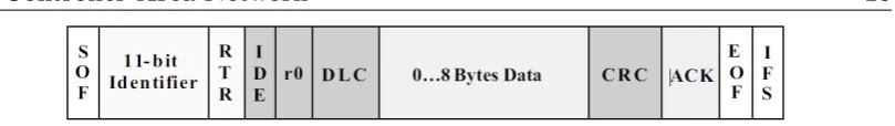
2.3.3 Frame Format
2.3 Controller Area Network 10
Figure 2.1: CAN Frame - 11bit Identifier (adapted from (Corrigan 2008a)).
The key difference between the two addressing modes is the increased identifier size.
Figure 2.2: CAN Frame - 11bit Identifier (adapted from (Corrigan 2008a)).
Data Frames are the most common frame format and is of the form shown in Figure 2.1 and Figure 2.2.Remote frames are used when a node wants to request information from another node. The composition is similar to the data frame with two exceptions. The RTR bit in the arbitration field is marked as recessive to indicate a remote frame and there will be no data. An error frame is transmitted when a node detects an error in a message. The other nodes on the bus will respond by sending error frames of their own. There are safeguards in place to ensure that repeated transmissions of errors do not completely congest the bus. The overload frame is primarily used to provide a delay between messages in the event that a node is too busy. It has a similar format to the error frame.
[image:26.595.127.463.194.233.2]2.4 Modbus 11
2.4
Modbus
Modbus was created in 1979 by Modicon and was a propriety protocol designed for
communication between Modicon Programmable Logic Controllers (PLCs) (de Sousa
& Portugal 2011). Modbus was effectively the first ever industrial field bus protocol (Hui, Hao & Daogang 2013). Modicon openly published the protocol and it remains free to use, resulting in Modbus becoming the first de facto standard for industrial commu-nications. Today it is maintained by Modbus-IDA, is still used widely in industry and continues to evolve (de Sousa & Portugal 2011).
2.4.1 General Modbus Features
Modbus is free and as such is one of the most widely used protocols across many industries. It is used with sensors and actuators that are network enabled. It is also used with more complex automation equipment such as RTUs, PLCs, human machine interfaces (HMIs) and supervisory control and data acquisition (SCADA) systems (de Sousa & Portugal 2011). Most of these implementations would be either on 485 or TCP networks. RS-232 Modbus implementations are limited to point-to-point connections, such as HMI to PLC (Thomas 2008).
2.4 Modbus 12
Table 2.1: Modbus memory organisation
Name Memory range Number of bits Functionality
Input registers 1(0)-65,536 (65,535) 16 Read
Holding registers 1(0)-65,536 (65,535) 16 Read and Write
Discrete inputs 1(0)-65,536 (65,535) 1 Read
Coils 1(0)-65,536 (65,535) 1 Read and Write
Modbus allows devices to read and write data to memory locations on another device. The device performing the reading and writing will have some processing ability (such as a PLC) but the device being written to and read does not need processing ability (such as a sensor), although it may have some. Modbus uses the client-server model. The device processing is the client and it makes requests to the server. The server never initiates an exchange. Clients can make multiple requests to multiple distinct servers one at a time. The specification does not allow for servers to have more than one client, but it is possible. Some devices acting as servers may have the ability to process simultaneous requests but it is generally done sequentially (de Sousa & Portugal 2011, Modbus Org 2006c).
The reading and writing functions are carried out in the memory of the server. The protocol defines the organisation of this memory but customisation is allowable (Modbus Org 2006c). Table 2.1 gives an overview of the specified organisation scheme. Note that the figures in the table are theoretical only. Many devices will have a memory range lower than specified here. Typically analogue inputs and outputs are handled through the registers and the digital inputs and outputs through the discrete inputs and coils.
2.4 Modbus 13 example follows:
To read coils 5-10 (hexadecimal and begins at zero) from slave 11 the query is as follows:
Slave address: 0A
Function: 01
Address high: 00
Address low: 04
Number of points high: 00
Number of points low: 06
The response from the slave follows a similar format but is not the focus given the bridge is a master only. The query forms the data portion of the Modbus frames discussed next.
2.4.2 Frame Format
The implementations have similarities in their frame composition. They both include the function code and data fields.
Figure 2.3: Modbus RTU Frame (adapted from (Thomas 2008)).
Each implementation has an address and error checking field. The ASCII frame also has the explicit start bit (:) and end bits (carriage return and line feed). Figure 3 shows the format for an RTU frame and Figure 4 shows the format for an ASCII frame.
Figure 2.4: Modbus ASCII Frame (adapted from (Thomas 2008)).
2.4 Modbus 14
2.4.3 RTU, ASCII and TCP
RTU and ASCII are asynchronous protocols that are implemented on serial channels, generally either EIA/TIA-232 (RS-232) or EIA/TIA-485 (RS-485). They are designed to be used on a physical bus with the slaves and master connected to the trunk. Both transfer a start bit as part of the frame. They differ in the way the frames are constructed and the way data is represented. RTU mode uses binary encoding and does not use delimiters (headers and trailers). ASCII encodes the data as ASCII characters and does use delimiters (Modbus Org 2006b). To compensate for the lack of delimiters while in RTU mode, timing limits between characters and frames are used. A no signal period of at least 3.5 character times between frames acts like the delimiter in RTU mode. In ASCII mode frames have a header and trailer. The : character is the delimiter in ASCII mode (de Sousa & Portugal 2011). Frame composition is considered later.
There are limitations on both serial variants of the protocol. Since the protocol was conceived in 1979 data types officially supported are limited to those available at the time (Modbus Org 2006c). It is possible to work around solutions to cater for modern formats such as using two 16 bit registers to store 32 bit values. There are also no security features inherent to the protocol.
2.5 Bridging the Protocols 15
2.5
Bridging the Protocols
Creating bridges or similar devices to link dissimilar protocols is not a new principle. Several papers have been written that explore the merging of CAN bus and Modbus (REF). There are also four companies that the writer is aware of that produce existing devices for this purpose.
2.5.1 Previous Works
A very brief paper by Guohuan, Hao & Wei (2009) identified the spread of fieldbus tech-nology in many industries and applications as well as the incompatibility of the many existing standards and protocols. They briefly discuss the two protocols and then de-velop a design for the protocol conversion interface. The hardware design identifies five components inside a block diagram; MAX232 as the serial interface, a PIC18F458 as the microprocessor, two 6N137 optocouplers chips to isolate each bus driver from the proces-sor, and an MCP2551 for the differential bus driving capabilities for CAN. The software design is only developed for the case of CAN as a master and Modbus as a slave. The brief description and a flowchart demonstrate the process at a high level of abstraction.
Wang, Zhang, Li & Ren (2013) studied the design of an adapter for Low-voltage distri-bution systems in Intelligent Electric Grids. Modbus is identified as the low level control network protocol of choice in this application. The major issue identified with the adapter is the dissimilar data sizes between the two protocols. Wang also refers to other studies that state issues with existing products. They claim that these devices do not properly take into account the data size problem. They may be able to transmit more than the 8 byte limit imposed by CAN but have issues with frame loss during communication. The articles referenced were not locatable to confirm the information, however, the frame size incompatibility is well known to the author. The rest of the paper outlines the selected hardware as well as the process required for developing the software.
2.5 Bridging the Protocols 16 down to just the data before being transmitted on the CAN bus.
The second major challenge addressed by software design is the issue of CAN data sizes. Wang applies techniques from the sub-packaging rule defined in Ethernet to deconstruct frames at the CAN transmitter and reconstruct at the CAN receiver. The final consid-eration is the delay in frame sending from the CAN interface. Wang noted that frames would sometimes be lost when transmitting at high speed. To address the issue a delay time between sending frames was calculated. This was based on the bit timing of the CAN bus based upon the selected baud rate along with the bus state, the priority of the sending node and the delay time of transmission. The authors claimed that the device was built, tested and met the requirements of the low-voltage distribution system.
The most recent study known to the author focused upon an adaptation layer for Mod-bus to CAN (Cena, Bertolotti, Hu & Valenzano 2014). The paper discussed how the traditional Modbus implementations’ speed limitations are potential issues, the introduc-tion of Modbus-TCP as a potential soluintroduc-tion and the idea of layering Modbus on top of other protocols as another solution. The theme of this paper is different to the others in that it is not a converter but a variation of Modbus similar to that of Modbus-TCP. CAN was chosen as it is simple, fast and many microcontrollers have CAN controllers built in. The adaptation layer has significant differences to the proposed bridge in this project, however, the issue of large (greater than 8 bytes) Modbus data PDUs requiring fragmentation and reassembly for transmission on CAN is evident. The solution engaged to solve the fragmentation-reassembly issue was to change the composition of the CAN data frames. In the first transmission of a Modbus frame over CAN, 2 bits at the start of the data field are reserved for identifying the protocol and the length of the Modbus frame. Subsequent frames in the sequence gain back the two header bits for data since these fields are constant for any one Modbus message. The CAN CRC field is used in place of the Modbus CRC field which is parsed from the Modbus frame. While similarities are identifiable in this paper, the differences between a bridge or protocol converter and an adaptation layer are significant and much of the rest of Cena is largely inapplicable.
2.5.2 Lessons from Previous Works
2.5 Bridging the Protocols 17 There needs to be a method of reducing Modbus PDUs of up to 252 bytes into 8 bytes or less size for transmission. The solution posed in (Guohuan et al. 2009) offers no detail beyond that of a flowchart. Wang et al. (2013) propose sending the whole Modbus without the CRC field (as CAN has its own comparable field) and then parsing the unrequired fields at the CAN receiving end. This method is not suitable to this project as there is no guarantee of control over the other CAN nodes on the network. Similarly, the adaptation layer proposed by (Cena et al. 2014) require configuration of the receiving CAN nodes and given the different nature of the protocol bridge and protocol adaptation layers is not optimal for this project.
Wang’s lesson regarding the mapping errors when simply stripping the data out of the Modbus frames is noted. The issue may be less pronounced on the buses the bridge will operate on. Testing may reveal if this is an issue.
There are two basic ways of achieving CAN transmissions using microcontrollers; using a microcontroller with embedded CAN controller and external CAN transceiver, or using a microcontroller with external CAN controller and external CAN transceiver. All papers reviewed suggest the former as the ideal path to take due to ease with implementations and hardware design. Using optocouplers to isolate the microcontroller from the transmission devices is also identified as desirable.
2.5.3 Existing Bridges and Available Products
Considering existing products is important. It allows appreciation for what has been achieved and may also help identify areas for improvement. It is highly unlikely that any of the products identified in this section would be suitable for the exact use intended for the network bridge. Ultimately, GDA would like a product developed internally. This allows for consistency in products and gives the opportunity to expand aspects of the network bridge into other products or applications if desirable.
Anybus Communicator from HMS
2.5 Bridging the Protocols 18 messaging that is configured through a graphical user interface (GUI). It supports both CAN standards 2.0A and 2.0B as well as serial communication standards RS-485 and RS-232. This product was designed to be used in fieldbus setups involving PLCs. It may require significant adaptation for it to function correctly in the BMS environment. It can only function as a Modbus slave. The obvious major drawback is the intended market for this device. It was designed for fieldbus use it may not interface as desired with BMSs expected for the network bridge (HMS 2015). In terms of general functionality the only significant improvement would be to add Modbus master capabilities.
CAN/Modbus Converters from ADF Web
ADF web offers several products in this category. There are Modbus TCP solutions that will not be considered and four different Modbus serial offerings. Electronically there are two variants; one is a Modbus master and the other is Modbus slave. The other two products are the same devices with extra galvanic isolation and a different enclosure. Each device has RS-232 and RS-485 connection and one CAN port. They support data rates on the CAN side up to the limit (1Mbps) and on the Modbus side up to the limit (115kbps) from the official standard. The devices are fully two directional messaging capable. Each device is only capable of being either a Modbus master or slave and not both (ADF web 2015). This may not be suitable for this task. Further, to use these devices requires the use of Windows based propriety software from ADF web called Compositor SW67011. The biggest improvement would be to have the configuration built into the device to remove the need for external software. Providing an interface to the device that allows on the fly configuration is consistent with practices at GDA. More flexibility with regards to Modbus configuration would also be desirable.
Modbus RTU to CAN converter from ICP DAS
2.5 Bridging the Protocols 19 directly (ICP DAS USA 2015). To be useful in this task, this device would ideally need support for Modbus ASCII and the ability to configure as a Modbus slave. Configuration would be better achieved with an interface on the device itself.
2.6 Constraints 20
2.6
Constraints
As a sponsored project the network bridge design must be carried out within the con-straints of the host organisation and within their requirements. Below is a description of those constraints and requirements.
As a potential commercial product, the bridge must be financially viable. When selecting components for use in the bridge they must be approved by GDA from a cost perspec-tive. All components in this project have successfully passed through this process. If a component to be specified is similar to one used on another existing GDA product, it may be used on the network bridge to help reduce stocking costs and make use of existing expertise within the organisation.
The development environment used in this project was chosen as it is the current envi-ronment employed by GDA. This includes the development board, microprocessor, pro-gramming language and compiler. Finally, GDA’s general design guidelines were followed regarding component choice and software design methodology where possible.
There is also a design considerations to be stated. Modbus frames can theoretically contain data up to 508 bytes in length. In the specific application of the bridge within GDA, this is unlikely to be the case. Discussions with GDA engineers suggest it is reasonable to assume that data requirements will not exceed 16 bytes.
2.7
Chapter Summary
Chapter 3
3.1 Chapter Overview 22
3.1
Chapter Overview
The basic principle is to keep it as simple as possible whilst meeting the requirements previously outlined. Hardware design is more restrictive as it is not as simple to create basic design to build on. The final hardware design must be of commercial quality. Therefore the design of the hardware will be conducted with the aim of producing one finished product which can then be produced as a printed circuit board (PCB).
The hardware design methodology involves smaller increments leading to a complete design. Each logical section, such as the Modbus interface, is broken down and designed separately. Existing library functions will be used from the chosen compiler to prove concepts where possible. Only once all concepts are proven will more advanced techniques be use to refine the design.
3.2 Equipment 23
3.2
Equipment
The following is a run-down of the equipment used during this project. This list is not exhaustive but highlights the key tools used.
As previously mentioned the development environment used was consistent with GDA practices. The development board used was an EasyPIC Pro v7 from MikroElektron-ika. A PIC 18F87K22 microprocessor was used in development and in final design as discussed later. The EasyPIC Pro board supports UART over universal serial bus (USB) natively and this was used for serial communications. A 3.3V CANSpi click board was used in conjunction with the development board to provide the CAN interface. During testing, two 5V CANSpi modules were also used. To view activity on the buses, a UNIT UTD2102CEL 100MHz digital storage oscilloscope was used.
Windows 7 based personal computers (PC) were used to run the development environment and simulation software for Modbus and CAN. USB cables were used to connect the USB UART module of the development board to the PC. During initial testing, the two 5V CANSpi modules were used. Later on a USB-CAN Converter from ICP-DAS, Inc was used to simulate a CAN node. This was done so that testing was not performed on two devices created during the project. Using external devices that are rated as per the communication standards validates testing results. The converter translates CAN messages to USB so they may be interacted with via PC. 15cm male-male breadboarding wires were used as the CAN transmission lines. Short wires were used to avoid reflections and other physical effects on the line.
3.3 Hardware Design 24
3.3
Hardware Design
Some of the traditional design choices are forgone here for the benefits of using tried and tested equipment already available at GDA. Technical functionality is the key requirement and should be observed first. Where possible, components used in existing GDA products may be used if they meet the specification and it provides benefit to GDA through reduced stocking costs or product familiarity. This is true regardless of whether the component selected is not the ideal selection based on other criteria. As a general rule, where two or more components meet all the requirements laid out, the cheapest component shall be selected.
The other major design consideration is alignment with the software development environ-ment. The circuitry found on the EasyPic Pro and add-on boards has proven functionality. It makes sense to utilise these circuits as a template for two reasons; they are proven to work and take away much of the risk of trying new methods, and they make the transfer of software from the development environment to the final product much simpler. Minor changes to microprocessor pin configurations will be required1.
Data-sheets for all devices mentioned by name in this section can be found in appendix G.
3.3.1 Microprocessor
The microprocessor is the central cog in the design. It affects the choice of all other components. Selection of the device was largely driven by GDA. The desire was to use a processor already deployed in other products and suitable for future commercial products. GDA favours the PIC range of processors from MikroElektronika. The device still needed to conform to the following requirements:
1. Ability to process CAN messages at data rates up to 1 Mbits per second and serial messages up to 19.2 kbits per second.
2. Sufficient memory to buffer communications data and serve other functionalities defined in ancillary circuitry later in the chapter.
3. Sufficient pins to service all functions of the bridge.
1
3.3 Hardware Design 25 4. Be available to use on the intended development equipment and with the selected
compiler and design environment.
Items one and two are critical in that they will affect the performance of the bridge’s main functions. Item four is required so that the software design will integrate with the hardware design correctly. Selectable PIC processors for this task far exceed the requirements of item one. Below is a conservative calculation of the required memory space:
Let’s assume that we need to buffer at any one time ten Modbus messages and ten CAN messages. The non-data portions of the CAN frames will be filtered by the hardware for us. We may need to buffer the entire Modbus frames. CAN frame requirements would be:
M emcan = 8bytes×10 = 80bytes (3.1)
This is fairly insignificant. Now we consider the modbus requirements. From figure 2.4, we see a the maximum size of a complete Modbus ASCII frame is 513 bytes. So:
M emasc = 513bytes×10 = 5,130bytes (3.2)
We need at least 5.2 kbytes of memory for buffering alone using this conservative approach.
The microprocessor selected was a PIC 18F87K22 which operates up to 64MHz, supports up to 128k bytes program memory, has 80 pins and is a supported chip on the selected development board. The processor is to be operated at 5 volts.
3.3.2 CAN Interface
Using a PIC processor as the central processor for the network bridge gives two clear options for implementing the CAN interface; select a PIC processor with an in-built CAN module or select a PIC processor with an SPI module and utilise an external CAN-SPI
integrated circuit to allow the processor and CAN transceiver to communicate. The
3.3 Hardware Design 26 In order to make the individual modules of the network bridge more portable, it was decided to use an external CAN device. The transceiver chip selected needed to support the full ISO standards (usually referred to as CAN 2.0A and 2.0B in datasheets). It also has to operate on the same supply voltage as the processor. In total, two CAN devices are required; a CAN-SPI conversion integrate circuit (IC) and a CAN transceiver IC.
The devices selected were the MCP2515 and MCP2551 from Microchip. The SPI module of the processor was used to communicate with the MCP2551 transceiver via the MCP2515 chip. Supporting circuitry was selected using the 3.3V CANSpi click board as a guide.
3.3.3 Serial Interface
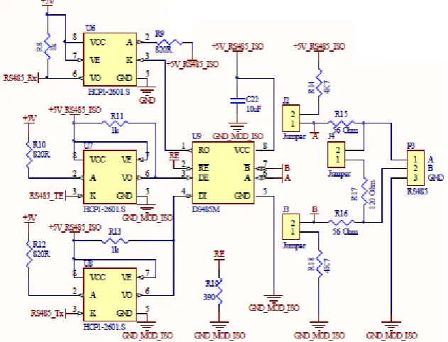
To enable Modbus communication the bridge requires a serial interface. The physical layer chosen for this project was RS-4852. This implementation required a transceiver to convert signals from the processor to the correct levels for transmission on the serial bus.
The devices selected were DS485M from Texas Instruments. This is a product that had been used on a previous GDA product. Supporting circuitry was selected using the RS485 Click board from MikroElektronika as a guide.
3.3.4 Power Supply
There is no guarantee of the supply voltage from the Building Management System. GDA’s experience suggests that a 24V AC, 24V DC or lower voltage supply is likely. Dealing with AC and assuming that the 24V AC supply occasionally spikes at 30V RMS. The equation for the max voltage the power circuitry needs to with stand is:
Vmax = 30V ∗
√
2 = 42.43V (3.3)
The bridge’s functional circuitry is mostly digital so the supply requires rectification if the source is AC. A bridge rectifier diode IC was selected to perform this task. The device
2
UART is used for the software development stage and the final solution can be modified to make use
3.3 Hardware Design 27 chosen was the DF04S, which accepts input bridge voltages up to 280V and an average rectified forward current of 1.5A.
The next stage of the power supply design in the switching regulator. A linear power supply was not considered. A 5V linear regulator would use too much power and generate excessive heat considering the supply voltage could be as high as 24V. The regulator IC chosen was the LM2671 from Texas Instruments. This device can tolerate input voltages up to 45V, can supply 5V in a fixed output configuration and operates at 96% efficiency.
The final power consideration was analogue supply. The touch panel feedback is an
analogue signal connected to the processor. The analogue supply pin of the processor was connected. Low pass filtering components were added to reduce high frequency noise on the signals.
3.3.5 Isolation
Communication transmission lines from external sources could be the source of voltage or current spikes. It is therefore important to isolate the communication interfaces from the rest of the board circuitry for protection. In order to achieve this it was necessary to isolate power supplies for those interfaces as well.
Isolation of the CAN interface was achieved by placing optical isolation ICs between the MCP2515 CAN-SPI chip and the MCP2551 transceiver chip. Similarly, isolation of the Modbus interfaces was achieved by placing optical isolation ICs between the processor and the DS485M transceiver chip. The isolation ICs used were HCPL-2601S.
Optically isolated DC-DC regulators were used to isolate the power supplies for the com-munications on the board. They take the supply 5V and isolate it for CAN and Modbus to create separate power supplies. The isolated DC-DC converters ICs used were ROE-0505S.
3.3.6 Ancillary Circuitry
3.3 Hardware Design 28 was designed to take over the supply of power when the standard supply dropped below a certain level. A test point was added and connected to a processor pin for determination of this level. This allows the bridge to self diagnose a power fault back to the BMS so that it may be attended to. A battery test point was also added to provide battery level feedback.
Five LEDs were included in the design for use as indicators. A power LED is lit when the bridge power supply is active. There are two LEDs for Modbus communications; one for transmission and one for reception. They are intended to illuminate when the RS-485 transceiver is operating. Similarly, the CAN communication has one LED indicating bus activity3. The final LED is for error reporting. With the exception of the power LED, all
LEDs are connected to the processor and their operation is to be configured in software.
The bridge design includes a Graphical Liquid Crystal Display (GLCD) and touch screen combination for use as a human-machine interface. The design used is adapted directly from the EasyPic Pro v7 development board but is arranged on different pins. To specify the limiting resistor for the supply voltage, the development board current was measured using a multi-meter. The value of the resistor used on the bridge was adjusted to reflect the 6V supply.
The operation of these devices are to be configured in software.
Numerous capacitors were used in the design of the bridge. Many were selected by
following recommendations from chip manufactures for use with ICs or the processor such as decoupling capacitors. Some were also included due to the potential for long track lengths on the PCB and the high frequencies encountered. Much of this part of the design was carried out under guidance from GDA engineers rather than driven by research carried out by the writer.
3One LED is sufficient since CAN is a differential system where both lines are used for transmission
3.3 Hardware Design 29
3.3.7 Printed Circtuit Board
PCB arrangement was focussed on having the functionalities of the board in separate areas. This was compounded by the use of isolation. Two layers were used; top and bottom. The processor was located centrally and its decoupling capacitors and crystal nearby. The power supply was placed at the bottom of the board. The CAN interface and its isolated power supply were located to one side of the board. Likewise with the Modbus circuitry to the other side. The communication headers were placed opposite each other for aesthetics. Keep-out sections were placed around each of the communica-tions interfaces containing the isolated components. Thick tracks were run through the middle of the board for high current transfer. Three main ground planes were placed; a standard ground plane and separate isolated ground planes for each of the communication interfaces. Two smaller ground planes were also placed around each of the oscillators. The GLCD was placed on the top layer as it is intended to be embedded in the lid of the encapsulation. The LEDs are also located on the top layer. All headers and the contrast potentiometer for the GLCD were located on the bottom layer since it is the accessible side of the board post installation4.
Ideally all tracks would have been placed manually but time restraints did not allow this. Some of the important track laying was carried out by hand but some use of Altium’s auto-route feature were utilised.
4
3.4 Software Design 30
3.4
Software Design
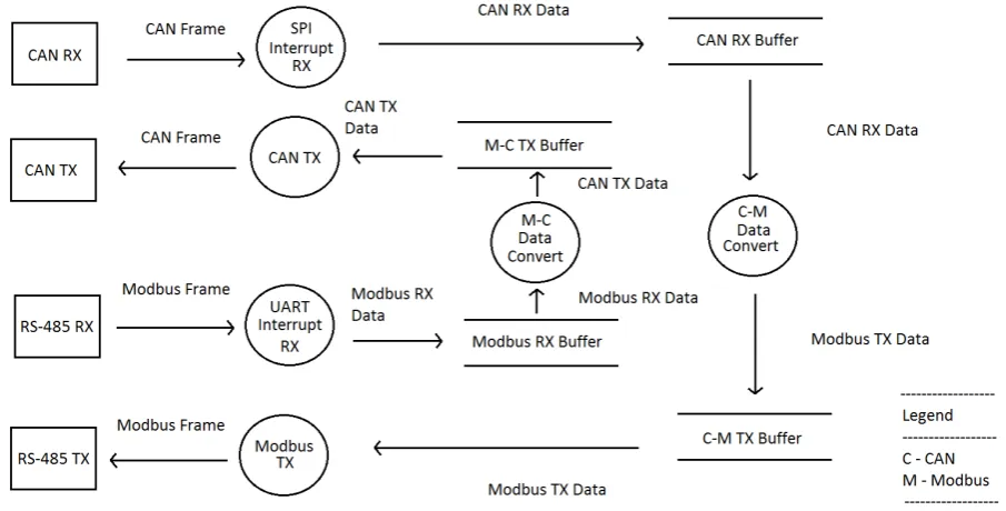
The key software design principle is modularity. Ideally, GDA will be able to use separate modules of this bridge in other projects. Where feasible, code was written in separate ’C’ files and combined using a header file inside a project. The design of the software was approached on two levels; an overview of the whole bridge functionality illustrated using data flows and then by considering the protocol implementations.
Logically, the bridge is both a CAN node and a Modbus ASCII master. CAN message handling and Modbus message handling are established separately first. Interrupt sources were to be used to receive messages and forward the data out of the other interface.
To visualise the process and also to aid development, a data flow diagrams (DFD) was created to show the bridge operation. The figure can be found in chapter 4.
3.4.1 CAN Interface
MikroC Pro comes with a CANSpi library containing a suite of functions for the ini-tialisation and operation of a CANSpi module attached to a PIC processor. The initial design idea was to use an SPI interrupt to start the processing of a CAN message using the library functions. CAN reception and transmission would be handled inside interrupt routines. During testing this was found not to be possible and will be discussed in the relevant chapter. A minor change was required. The interrupt routines were configured to set flags that were processed in the main loop. Again during testing this was proven ineffective for the CAN communications. Eventually the entire CAN functionality was moved to the main function of the project. All initialisation and message handling was processed there. For proof of concept, arbitrary configurations were used on the bridge. Testing of the CAN interface was undertaken using the USB-CAN converter.
3.4.2 Modbus Interface
3.4 Software Design 31 RS-485 which is overlaid onto the UART. The bridge was designed using UART and the RS-485 implementation would only occur on the finished bridge (PCB).
The bridge is not a typical Modbus master. The logic for operation is not configured on the bridge itself. This would be performed on the BMS CAN node. The bridge needs only to communicate with a Modbus slave and report errors such as time-out and is not required to poll directly. Facilitation of the communications was divided into five key functions:
1. Serial Transmit
2. Modbus Transmit
3. Serial Receive
4. Modbus Receive
5. Longitudinal Redundancy Check (LRC)
The serial functions were developed first. To test their functionality the terminal window in MikroC was used to send and receive UART communications. Once the serial functions worked as desired, the Modbus functionality was created. Transmission was achieved first by creating a function that took the data and encased it in a Modbus frame. Then the Modbus receive functionality was created by coding a reversing of that process. Initially, both were tested using the terminal. The LRC was the last function created as it required working send and receive functions. Hand calculations were performed on messages sent to ensure that the LRC was accurate.
3.4.3 Ancillary Functions
This section is devoted to the functionality not strictly related to one protocol or the other. These are functions which support the translation between the two. CAN data is treated as numeric but Modbus ASCII encodes as ASCII. An ASCII to Hex and Hex to ASCII set of functions were created to allow the transition between the two encoding schemes. A simple example follows:
3.4 Software Design 32 to convert each character into two characters, ’2’ and ’D’. ’2’ will be encoded as 0x32 and ’D’ will be encoded as 0x44. These values are taken from the ASCII table.
Functions were created to automate this process as well as its inverse. In order to separate two digit hexadecimal numbers into a pair of single digit hexadecimal numbers, two functions were written.
The literature shows the incompatibility in data sizes between the two protocols. A method was required to successfully decompose and reconstitute Modbus frames with data lengths of greater than 8 bytes into two or more CAN frames. Due to reasons discussed in later sections, this was not implemented. The designed principle for this is discussed in the next chapter.
3.4.4 Main
The original design of the main function was to initialise the communications modules and provide GLCD functionality and LED indications. During the design it was noted
that the interrupt implementation of CAN proposed would not work. Interrupt flag
3.5 Proposed Testing Methodology 33
3.5
Proposed Testing Methodology
The bridge’s functionality needs to be verified. A testing procedure was developed with the aim of determining the capabilities of the bridge, its limitations and where it can be improved.
This section is an outline of the intended testing procedure.
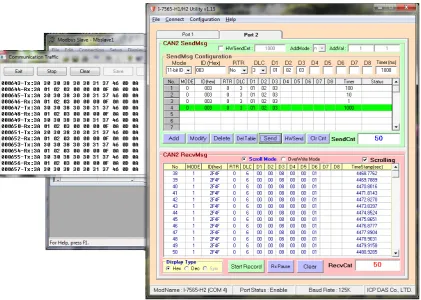
To be satisfied that the CAN and Modbus functionalities work as desired they must be able to communicate with devices that conform with their standards. A series of tests were designed to assess the performance of the bridge. All CAN related testing will be conducted using the USB-CAN converter to simulate the BMS CAN node. Modbusslave will be used to simulate the Modbus ASCII slave. The first test is to verify the concept. The bridge should:
1. Receive a CAN frame
2. Extract the data
3. Put the data in a Modbus frame and send it
4. Receive a Modbus frame back and extract the new data
5. Put the new data into a CAN frame and send it back to the originating CAN node.
The device needs to successfully complete this test as the first stage. The parameters of each protocol such as speed, filters, flags etcetera can be selected arbitrarily. The test should be performed separately using the 11bit and the 29bit CAN identifiers to ensure compliance with both standards (2.0A and 2.0B).
After successful completion of the first test the bridge should use the same testing proce-dure to confirm that the bridge operates fully over the range of possible communication speeds. This means up to 1Mbit on the CAN side and 19.2kbit on the Modbus side. Each extreme from both protocols should be tested with each other, i.e. max CAN speed with minimum Modbus speed etc. These tests will confirm whether the bridge can function over the baud ranges given in the protocol standards.
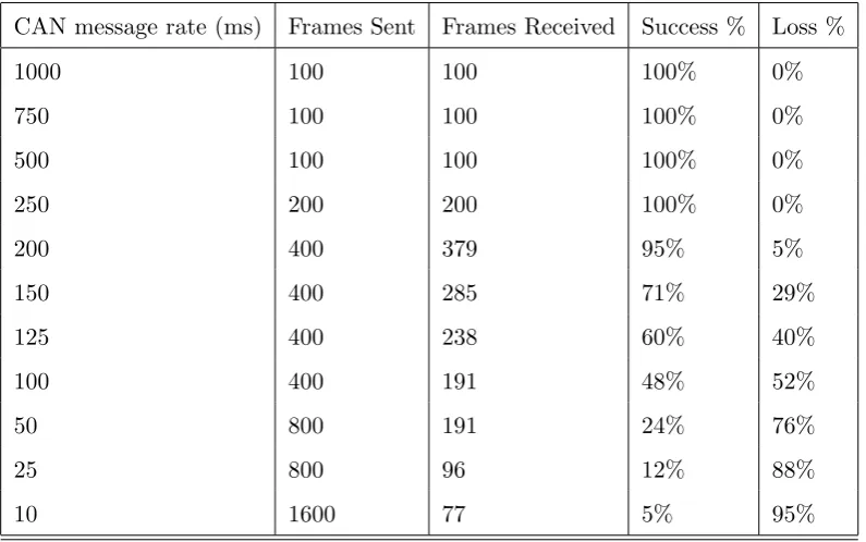
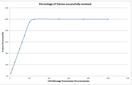
3.5 Proposed Testing Methodology 34 from the USB-CAN converter dependant on the BMS messaging rate. The faster the rate, the more messages that will be sent. A count of the number of frames that the BMS CAN nodes send and receive will be kept. The success ratio is the number of frames received divided by the number of frames sent. These results should be tabulated as percentages and graphed for analysis.
Testing should be performed at differing baud rates to determine how the bridge performs over the range of specified operation speeds. Four sets of parameters are to be used:
1. Maximum CAN baud and maximum Modbus baud
2. Minimum CAN baud and minimum Modbus baud;
3. Maximum CAN baud and minimum Modbus baud;
4. Minimum CAN baud and maximum Modbus baud
Performing the testing at the extremes will allow the performance of the bridge to be specifiable within the boundary of those results.
3.5.1 RS485 Confirmation
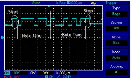
There was no RS-485 enabled Modbus ASCII slave device to test with during the project. The hardware design was adapted from the 3.3V RS-485 Click board from MikroElek-tronika (MikroeElekMikroElek-tronika 2012b). In order to prove the hardware concept of the serial interface, testing was carried out using a RS-485 click board and an oscilloscope. The RS-485 was connected to a bread board and terminated using a 120 ohm resistor. A successful test would be achieved by the observation of an RS-485 master packet on the bus. A photograph of the testing set-up with the bread board, terminating resistor and oscilloscope can be found in appendix F.
3.5.2 Physical Cable Testing
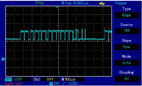
3.6 Chapter Summary 35 ten meter lengths of twisted pair (as per the CAN physical specification). Measurements were taken with an oscilloscope. If transmission lines were the cause of CAN transmission errors, these tests would show evidence of abnormal signal levels. This may include overshoot, jitter, ringing etcetera.
3.6
Chapter Summary
Chapter 4
4.1 Chapter Overview 37
4.1
Chapter Overview
This chapter details the hardware and software design elements of the network bridge. It is worth re-iterating that several hardware components included in the design do not have accompanying software elements. The bridge is to be expanded and developed further as a commercial product and this requires a complete hardware base. Figure 4.1 shows the overall logical design of the bridge. It is to operate as a CAN node and Modbus ASCII master simultaneously.
4.2 Hardware Design 38
4.2
Hardware Design
The hardware design process had two distinct phases; the schematic design and the PCB layout. Each functional subsection of the bridge is detailed using focussed versions of the schematic found in appendix E. This design will consider the major components of the design and will not focus on simpler features such as current limiting resistors or decoupling capacitors.
The final section will include the PCB layout of the bridge and justify the positioning of components on the board. All ICs included in this design have selected extracts from their data-sheets located in appendix G.
4.2.1 Microprocessor
The oscillator chosen is a 14.7456MHz crystal. The rationale for this selection was to use a crystal with a frequency wholly divisible by 9600. This allows the UART to generate the required bauds without error. Using crystals with non-divisible frequencies can cause issues that will be discussed in a later chapter. The timing of the CAN-SPI interface is set by the crystal connected to the MCP2515 IC and is not affected by this selection.
The programming header P2 is connected to SPI pins on the PIC to allow programming. The MCLR pin is arranged with resistors R2, R1 and capacitor C35 to give a time constant matched to the start-up time of the processor.
The processor data-sheet recommends 100nF capacitors for decoupling between the pos-itive voltage pins and their associated grounded pins. Additional 10uF capacitors were also included due to the high power requirements of the optical isolation employed on the bridge. The value used was recommended by the GDA engineers.
4.2.2 CAN Interface
4.2 Hardware Design 39 via the HCPI-2601S optical isolators. The isolated supply voltage and ground can also be observed. This will be discussed in a later section. The header P4 is for connection of the transmission lines. They are labelled CAN high and low and should only be connected as such. The CAN interface is shown in figure 4.2.
Figure 4.2: CAN Communications Hardware Interface
4.2.3 Serial Interface
Figure 4.3: Serial Communications Hardware Interface
4.2 Hardware Design 40 communicate with the processor through the HCPI-2601S optical isolation chips. These are the transmit enable pin and the two data pins (receive [RO] and transmit [DE]). The receive enable pin is held low (on) via R19, a 390 ohm resistor. The intent is to use this as a troubleshooting feature for transmission as the internal circuity of the DS485M will mean transmitted messages will echo on the reception input. The jumpers J2 and J3 can be used to stop the transmission lines floating, which can create noise on the bus1. Jumper J4 is used to enable a termination resistor when the bridge will be acting as the first or last node on the bus. The header P3 is the transmission line connection for the RS-485 bus.
4.2.4 Power Supply
Power to the bridge is supplied into P1. The bridge expects up to 24V that could be DC or AC. Rectification is provided by the DF04S bridge rectifier. The rectified voltage is passed to the LM2671 switching regulator. This device is configured to produce 6V. This will allow the expected 1V drop across the diodes D4-D6 to produce 5V. All components selected were specified using the data-sheet as a guide.
Figure 4.4: Power Supply Hardware
The processor is supplied from net VMI (the cathode end of D5 and D6). The commu-nications interfaces are supplied from the output side of the voltage regulator U3. This device has a rated drop-out of 40mV at 250mA essentially making the output voltage the same as the input. The enable pin is connected to pin 27 on the processor. The rationale is that this gives control of the power supply to the non-processor components of the bridge to the processor. During a power outage, non-critical components can be disabled and the processor put in sleep mode to prolong the life of the battery. The advantage of
1The calculation for this resistor value in the datasheet recommends a lower value than used. The
4.2 Hardware Design 41 this strategy is that the processor will not require a reset and allows a diagnostic message to be sent from the bridge to the BMS informing of a power outage. The diodes D3, D4, D5 and D6 are required to prevent current draw into the regulator U2 or charging of the battery.
The analogue supply is required for operation of the touch panel. The inductor L2 is for low pass filtering of the analogue supply.
The isolated DC-DC converters U4 and U5 are for the CAN and Modbus isolated power supplies.
4.2.5 Isolation
There are two isolation approaches present; the power isolation and the data isolation. The data isolation refers to the HCP1-2601S optical isolators between the CAN and RS-485 transceivers and the MCP2515 IC or processor respectively. These devices protect the data lines of the communications interfaces. The isolated supplies provide power to the communication circuitry on the outside edge side of the optical isolators.
4.2.6 Ancillary Circuitry
LED D11 is used to indicate power to the bridge. D7 is an indicator of serial reception. D8 is an indicator of serial transmission. D9 indicates when there is activity on the CAN bus. D10 is designed for use in fault indication. All LEDs bar D11 are software configured. The communication indicator diodes are to be powered when the relevant activity occurs on the buses. D10 is flexible and may be configured to meet user needs.
4.2 Hardware Design 42 The GLCD and touch panel combination were used during design and testing. The imple-mentation used for the bridge is a near replica of the circuitry found on the development board. Component R25 has been adjusted to account for the change in input voltage. The calculations are below:
A 1.4V drop was measured across the resistor. Its value was 20ohms so
Ires= 1.4V /20Ω = 7mA (4.1)
The voltage drop will change as a result of the great supply voltage (6V) on the bridge giving a drop of
Vnew= 1.4 + 1 = 2.4V (4.2)
Now we can see the new value of resistance required to maintain a current similar to the original
Rnew= 2.4V /0.07A= 34.29Ω (4.3)
The next highest E12 series is selected at 39 Ohms. This is resistor R25.
4.2.7 Printed Circuit Board
The final PCB top and bottom layer layouts are found in appendix D. Appendix D also contains 3D visualisations of the PCB. Both the top and bottom layer have been utilised for ease of placement and aesthetics. Simple placement rules have been observed. The layout is broken up into functional elements; power supply, CAN interface, Modbus interface and the processor. The two communication interfaces are placed on either side of the board. Both of these sections are optically isolated, have their own ground planes and are bounded by keep-out sections. The power supply circuitry is located on the bottom of the board. Isolated power is kept to the edges of the board and away from non-isolated power. The processor is located centrally. Both crystal oscillators have ground planes surrounding them for shielding. The inductor L1 was placed safely away from the feedback of the regulator. Decoupling capacitors were placed near their respective ICs.
4.3 Software Design 44
4.3
Software Design
This section details the code written for the network bridge. All code referred to here can be located in appendix D. The modular approach to this software requires a header to tie the code together. The header file ProjectDevBoard contains the function prototypes for the project.
[image:60.595.85.538.324.554.2]The first element of the design is the data flow diagram. The DFD shown in figure 4.6 is the ideal DFD in that it assumes that serial peripheral interface (SPI) interrupts function correctly. The tested bridge does not have this functionality and it is replaced with a flag check within a continuous loop. The other processes, data stores and flows are not affected by this change.
4.3 Software Design 45 Modbus functionality is confined to the C file ’Modbus’. There are several variables within the global scope of the Modbus C file. The most important being the send and receive buffers and frame length storage. There are six modbus functions:
1. modbus init - Initialisation of the Modbus interface.
2. TX serial - Transmission of serial data.
3. TX modbus - Creation of Modbus transmission frames.
4. RX serial - Reception of serial data.
5. RX modbus - Checking of LRC from serial receptions and data extraction.
6. LRC - Calculates the longitudinal redundancy check of a frame.
The initialisation function sets up the UART with the correct parameters for Modbus communications. This includes the baud rate, synchronisation (asynchronous for Modbus) and number of data bits2.
The serial transmission function should only be called after the Modbus transmission function to ensure data integrity. As a result, the only function call is located inside the Modbus transmit function. It receives the size of the data to send as an argument. The send frame is put into the serial transmit register TXREG1, byte by byte until the full frame is sent.
The Modbus transmission function receives a buffer of data and the buffer length as arguments. An ASCII colon (hexadecimal 0x3A) is placed in position zero of the global send frame. The contents of the argument data frame are then copied to the global send frame. The LRC function is called and the result stored. Since the LRC will be a two byte result it has to be split into two ASCII characters. This is performed by the functions split first and split second. These two characters and the new line characters (ASCII CR and LF) are appended to the end of the global send frame. The function then calls TX serial to send the Modbus frame.
2Note that parity checking was not implemented due to reasons discussed later. However, instead of
the 7 data bits with a parity check required by the standard, 8 data bits with no parity was used since
4.3 Software Design 46 The first step in the serial reception function is to read the current byte off the UART. If a colon has previously been received the variable named Go will be in set mode (equal to one) and the function will extract the contents of the UART until the line feed character is received. If Go is not set (equal to zero) and a colon is received, Go will be set and the reception process can continue. Any other characters received in this circumstance will be ignored. A count of the number of bytes in the received Modbus frame is maintained for use in the RX modbus function.
The Modbus receive function copies the serial frame into a holding array ignoring the colon character. The LRC of the received message is then checked and if correct, the data only portion of the frame is placed back in the reception array3.<