White Rose Research Online URL for this paper:
http://eprints.whiterose.ac.uk/131696/
Version: Accepted Version
Article:
Khan, Z. and Benaissa, M. orcid.org/0000-0001-7524-9116 (2015)
Throughput/Area-efficient ECC Processor Using Montgomery Point Multiplication on
FPGA. IEEE Transactions on Circuits and Systems II: Express Briefs, 62 (11). pp.
1078-1082. ISSN 1549-7747
https://doi.org/10.1109/TCSII.2015.2455992
[email protected] https://eprints.whiterose.ac.uk/
Reuse
Items deposited in White Rose Research Online are protected by copyright, with all rights reserved unless indicated otherwise. They may be downloaded and/or printed for private study, or other acts as permitted by national copyright laws. The publisher or other rights holders may allow further reproduction and re-use of the full text version. This is indicated by the licence information on the White Rose Research Online record for the item.
Takedown
If you consider content in White Rose Research Online to be in breach of UK law, please notify us by
"
Abstract—High throughput while maintaining low resource is a
key issue for Elliptic Curve Cryptography (ECC) hardware implementations in many applications. In this paper, an ECC processor architecture over Galois Fields is presented that achieves the best reported throughput/area performance on FPGA to date. A novel segmented pipelining digit serial multiplier is developed to speed up ECC point multiplication. To achieve low latency, a new combined algorithm is developed for point addition and point doubling with careful scheduling. A compact and flexible distributed RAM based memory unit design is developed to increase speed while keeping area low. Further optimisations were made via timing constraints and logic level modifications at the implementation level. The proposed architecture is implemented on Virtex4 (V4), Virtex5 (V5) and Virtex7 (V7) FPGA technologies and respectively achieved throughout/slice figures of 19.65, 65.30 and 64.48 (106/ (Seconds x Slices)).
Index Terms—Elliptic Curve Cryptography (ECC), Point
Multiplication (PM), Field Programmable Gate Array (FPGA), Throughput per Area (throughput/area), Efficiency.
I. INTRODUCTION
UBLIC key based information security networks use cryptography algorithms such as Elliptic Curve Cryptography (ECC) and RSA. ECC has emerged recently as an attractive replacement to the established RSA due to its superior strength-per-bit and reduced cost for equivalent security [1].High speed ECC is a requirement for matching real-time information security, however, in many applications the hardware resource implications may be prohibitive and the required high speed performance would need to be achieved within a restricted resource performance. FPGA based Hardware acceleration of ECC has seen a surge of interest recently. There are several state of the art FPGA implementations aimed at the high speed end of the design space [7 -13]. Most of these however use increased hardware resource to achieve the speed improvements sacrificing overall efficiency in terms of the throughput/area metric; such efficiency is desirable in many emerging low resource applications in particular in wireless communications. Area optimised high speed ECC design is challenging; there are requirements of algorithmic optimisation, careful scheduling to reduce clock cycles, size of multiplier, critical delay of the logic, andpipeliningissues [7], [9].
In ECC, scalar point multiplication (PM) is the main
Z. Uddin-Ahamed-Khan and M. Benaissa are with the Department of Electronic and Electrical Engineering, The University of Sheffield, Sheffield,
operation. The PM can be implemented over either prime fields, GF(p) or binary extension fields, GF(2m) adopting either
projective coordinates or affine coordinates. Binary extension fields called also finite fields (FFs) are more suited to hardware implementation due to their lower complexity FF multipliers, simple FF adder and single clocked FF squaring circuits. Projective coordinates are suited to throughput/area efficient ECC designs, where the costly inversion operation is avoided and the inversion operation required to convert projective into affine coordinates can be achieved by multiplicative inversion [2], [6]. ECC computations in the projective coordinates system are based on large operand finite field operations of which multiplication is the most frequently performed. The high speed performance of ECC designs therefore would depend mainly on the performance of the FF multipliers. Digit serial FF multipliers are often used to reduce latency; popular multipliers here include the direct method based multipliers and Karatsuba [7], [10]. If the field size is m and the digit size is w of a digit serial multiplier, then the number of clock cycles for each FF multiplication is s + c, where s = m/w, and c is for clock cycles due to data read-write operations. Thus, large digit multipliers can reduce clock cycles (latency) with increasing complexities of area and critical path delay. The critical path delay can be reduced using pipelining with some extra latency [9].
In this paper, we present an area-time (throughput/slice) efficient ECC processor over binary fields in projective coordinates on FPGA. We implement the Lopez-Dahab (LD) modified Montgomery algorithm for fast PM. We demonstrate
a new ‘no idle cycle” [7] combined point operations (point
addition and point doubling) algorithm to remove idle clock cycles in between two successive point operations. We schedule point operations very carefully to avoid the idle clock cycles due to data dependency, read-write operations, and pipelining. In addition, our efficient arithmetic circuit includesa digit serial multiplier, an adder and a square circuit. The presented arithmetic unit can support on-the-fly addition and square operations while performing FF multiplication. Moreover, we present an improved Most Significant Digit(MSD) serial multiplier utilizing segmented pipelining similar to the Least Significant Digit (LSD) multiplier presented in [2,4]. We develop an optimized distributed RAM based memory unit for flexible data access to support reduced data dependency in the arithmetic operations. Weadopt the Ithoh- Tsujii inversion algorithm for inversion to save area [5, 6]. Finally, we use a
S1 3JD, UK, (e-mail: [email protected] or [email protected]).
Throughput/Area Efficient ECC Processor on
FPGA
Zia-Uddin-Ahamed Khan,
Student Member, IEEE
, Mohammed Benaissa,
Senior Member, IEEE
dedicated finite state machine based control unit to speed up the control operations. The proposed architecture is implemented on different FPGA technologies, Virtex4 (V4), Virtex5 (V5) and Virtex7 (V7), and compared to state of the art in terms of a throughput/slices metric. The throughput/area performance in (1x10⁶/s)/(slices) of our proposed design (19.65 on V4, 65.30
onV5 and 64.70 on V7) outperforms state of art designs on FPGA to date.
The rest of the paper is organized as follows. Section II discusses preliminaries of PM, and the Lopez-Dahab modified Montgomery point multiplication in projective coordinates. Section III reviews resource constraints in high throughput ECC. Section IV illustrates the proposed design. Section V presents the results of the FPGA implementation and a comparison with recently published state of art designs on FPGAs, followed by conclusions in section VI.
II. PRELIMINARIES
A. ECC over GF(2m)
ECC over GF (2m) is suitable for hardware implementation.
The main operation of ECC is scalar point multiplication where is a scalar (integer), is a point on the elliptic curve, and is a new point of the curve after [2].
Let E be an elliptic curve in the binary extension field. E is defined by a set of points ( and ), and a point at infinity ∞, which satisfy the equation below:
(1) Where and are elements of the finite field, GF(2m) and
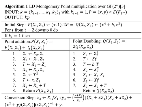
[2]. The point multiplication ( ) is accomplished by point addition and point doubling depending on , the th value of . The projective coordinates based Lopez-Dahab (LD) modified Montgomery point multiplication algorithm, as shown in Algorithm 1, has been adopted by many designs in the high performance ECC design [7-13] space due to its speed, side-channel attack resistance, suitability of parallelisation and is low resource friendly.
III. RESOURCE CONSTRAINED HIGH THROUGHPUT ECC
For a high throughput ECC implementation in the low area end
of the design space, there are requirements of optimization of the critical path of the logic, the area of the design, and number of clock cycles (latency) for the PM. Throughput is usually improved via the adoption of large digit size multiplication and parallel operation of multiplications to decrease the latency. However, these steps result in an increased area and critical path delay and therefore affect the throughput per area metric figure. The critical path delay can be minimised via pipelining [9] at the expense of an increase in area and number of clock cycles with the number of pipeline stages inserted in the design. Also, the pipeline stages can generate idle cycles in the data dependable field operations [7]. The number of pipeline stages is an important consideration for area optimized high speed design often requiring a latency versus clock frequency trade-off. The latency due to pipelining can affect the merits of the use of a large digit size multiplier and the parallelisation of multiplication. In general, the area complexity of a high speed ECC design would depend on the digit size of the multipliers used and the level of parallelism adopted, on the size and sophistication of the memory unit, and on the control unit.
IV. PROPOSED THROUGHPUT/AREA EFFICIENT ECC PROCESSOR
Our proposed area optimized high throughput architecture is presented in Fig.1. The design consists of an efficient arithmetic unit, an optimised memory unit and a dedicated control unit.
[image:3.595.305.551.99.284.2]A. Segmented Pipelining Based Digit Serial Multiplier The arithmetic unit consists of a novel most significant digit (MSD) serial multiplier, a square and adder circuit as shown in Fig.1. Digit serial multiplication for the high speed ECC implementation end tended to be either in direct form (i.e. MSD serial Multiplier) [10] or in bit parallel form (i.e. Karatsuba multiplier) [8], [9]. There are some advantages of Karatsuba multiplication over MSD multiplication. A Karatsuba FF multiplication takes s-1 cycles, where s = m/w, and is suitable for pipelining. An MSD FF multiplication takes m + 1 cycles where the extra clock cycle delay is due to the reduction register [2], [5] [9], and [10]. However, a pipelined Karatsuba Fig. 1. Proposed throughput/area efficient ECC architecture for n =2
Algorithm 1 LD Montgomery Point multiplication over GF(2 )[3]
INPUT: with
OUTPUT:
Initial Step:
For from downto 0 do If then
Point addition: Point Doubling:
1. 2. 3. 4. 5. 6. 7.
8. Return
1. 2. 3. 4. 5. 6. 7.
Return Conversion Step:
[image:3.595.54.279.103.265.2]multiplier based ECC implementation has been shown to achieve a lower clock frequency than a direct digit serial multiplier based implementation [7-8], [10].
For large MSD digit serial based ECC, pipelining is required which can affect latency in the point multiplications. In this work, we apply segmented pipelining to improve performance in MSD multiplication. In the segmented pipelining approach, a wxm digit serial multiplication is broken into sub digit serial multiplications called segmented multiplications w1xm,
w2xm,...,wnxm, where w=w1+w2+ …+ wn. The segmented
multiplication product is first saved in the register (Reg) before reduction into m bits using an interleaved reduction similar to that in the bit serial multiplier in [2]. The reduced m bit output of the reduction unit is saved in another Reg to use in the next cycles reduction or output. Thus, the proposed multiplication takes s +2 clock cycles where 1 extra clock cycle is due to the segmented pipelining, and the other additional clock cycle for pipelining after the reduction unit. A new input of the multiplier is inputted in every s clock cycles. Thus, a real time reset is required in every s cycles. We use multiplexers to select zero for reset and save one clock cycle for the FF multiplication. Finally, the segmented pipelined multiplier takes one clock cycle for n segmentations without increasing area (slices) on the FPGA. The unused flip flops (FFs) in the combinational circuit of the multiplier are utilized in the pipelining [8].
To evaluate our proposed segmented multiplier, area and time complexity analysis is performed and presented in Table 1 which also includes comparison to state of the art digit serial multipliers reported in [15],[16], and [17]. For or less, our proposed multiplier shows same or better latency using similar or less resources. However, a key advantage of our proposed architecture is that we are able to achieve higher speed for the same (or less) area and the same (or less) latency; this is because our critical path delay can be modulated by the number of segmentations (n) with extra Flip Flop (FFs). Thus, our
critical path delay can be optimised (to achieve the desirable high speed) by choosing an optimum number of segmentations (n). To generalise, from Table 1, the best figure latency for a
field multiplication [15,17] is 2 , our multiplier’s latency is
. As a rule of thumb, therefore as long as m<4d, our
multiplier would achieve comparable or better latency figure. But what is crucial is that for comparable (less or higher) latency say and same digit size, our design can achieves improved critical path delay, log in our case (due to GF2MUL) compared to log in [15.17], using an optimum segment size without increasing the latency of the multiplier. Thus, utilising similar area, our multiplier can achieve higher speed. At the extreme, the use a full precision multiplier with an optimised segmentation would thus lead to the highest speed.
B. Optimized Memory Unit.
High speed and flexible design for the memory unit can improve performance. We consider an optimised distributed RAM based memory unit. There is an 8xm size register file in a unit, one m bit register (accumulator) and one shift register (Shiftreg). The 8xm register file consists of one m bit input that can load data in any location of the register file, two m bit output buses (A bus and B bus) that can access data from any location of the register file. The shift register can store data from any location of the register file to provide w size digit (bi) multiplier for the FF multiplication. The accumulator can save a result from the arithmetic unit or new data from the register file to do a square operation. The accumulator and square circuit are connected such that repeated squaring can be done without saving in the register file. The repeated squaring improves latency of multiplicative inversion as proposed in [6]. The memory unit is smartly accessible to write, read shifting operation in any location. The easy accessibility of the memory reduces the number of temporary registers for the PM. The memory unit consumes very low area to provide high speed data access. LD Montgomery point multiplication as shown in algorithm 2.
To schedule for no idle cycles [7], we combine the point addition and point doubling algorithms for the current value of as shown in Algorithm 2. We observe that the product of the last multiplication is if or if . Thus, the first multiplication of the loop should be independent of the last multiplication. For example, if the last product is then TABLE I
LATENCY, CRITICAL PATH DELAYAND RESOURCESOF DIGIT SERIAL MULTIPLIERS OVER GF(2m)
Ref Latency, cc Critical path delay #XOR #AND #FFs, #Mux
[15] log C
[16] log ---
[17] log
Ours
log irreducible polynomial , k the is second higher order of s(m+d-1)+m-1, m
segments, d= digit size, .
Algorithm 2 Proposed combined loop operation of the LD Montgomery point multiplication with careful scheduling For from downto 0 do If then
If then If then
Point addition: and Point Doubling:
St1:
St2: ,
St1:
St2:
St3: , St4: .
St5: , . St6: .
the next operands of multiplication are and . Otherwise, the next operands will be and . Thus, the first multiplication depends on the last which means the bit as shown in Algorithm 2.
C. Scheduling for Point Operations
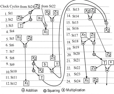
In this paper, we propose new scheduling in the combined Fig.2 illustrates the proposed schedule using a 41-bit digit size FF multiplier. The 41 bit digit size FF multiplier takes M = 4 cycles for actual multiplication, and c = 4, with 2 clock cycles for pipelining and 2 clock cycles for unloading from and loading to the memory unit. In a loop, the point operation in the projective coordinates system requires 6 multiplications. To ensure no idle state in the point multiplication, a new multiplication is started at every 4 clock cycles. Thus, two consequent but independent multiplications are overlapping
each other as shown in Fig. 2 for and . Again,
the adder circuit placed in the common data path is capable of doing addition concurrently. The square operation takes three cycles with1 cycle to save in the accumulator, 1 clock cycle for squaring, and 1 clock cycle for loading. Repeated squaring can be done without storing in the register file. Thus, double squaring takes 4 clock cycles.
V. IMPLEMENTATION ON FPGA AND RESULTS
Our proposed efficient ECC processor is implemented over GF(2163), GF(2233), GF(2283), GF(2409), and GF(2571), on
different FPGA technologies, namely Virtex4 (LX25_12 for f163, and LX100_12 for f233 to f571)), Virtex5 (XC5VLX50_3 for f163), and Virtex7 (Vx550T_3 for f163, and V585_T for f233 to f571 ) using Xilinx tools versions 13.2 and 14.5 respectively. The design was implemented on Virtex4 and Virtex5 technologies to allow for a fair comparison to most relevant works, and on the Virtex7 to evaluate the performance on the newer technology. The Xilinx tools were used to set high speed properties and put subsequent timing constraints to improve the area-time product. The implementation results after place and route of our ECC designs are summarized in
Table III. Table IV also includes area-time performance and comparison to state of the art.
As shown in Table IV, the main contribution of the segmentation in the multiplier is an increase in the clock frequency whileutilizing very small resources (FFs). The clock frequency for 3 segmented (3 Seg.) pipelined multipliers based ECC design is 290 MHz on the Virtex4- that is 38 MHz- more than the respective implementation of non-segmented (No Seg.) multiplier based ECC. Again, the 2 segmented (2 Seg.) pipelined multiplier based ECC shows the best throughput per slice (65.30) is implemented on Virtex5 the 3 segmented multiplier based ECC on Virtex7 shows the highest performance (only 10.51 µs for an ECC point multiplication).The optimum size of the segments is subject to a trial-error method to achieve high throughput.
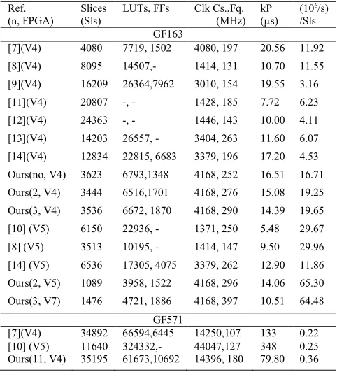
Table IV shows comparisons with relevant high performance ECC designs on FPGAs in term of efficiency metric throughput/area (( 1x10⁶/s)/slices) over GF(2163) and GF(2571).
For GF(2163) , the previous best optimised work was reported in
[7] where one 41bit pseudo-pipelined Karatsuba multiplier was used with a so called “no-idle cycles” point multiplication approach to achieve 11.92 throughput/area figure on Virtex4. Our no-segment based ECC design consumes less area (3623 slices) and achieves higher clock frequency (252 MHz) than [7] (4080 slices, 197 MHz) and therefore has a 40% higher throughput/area efficiency. Particularly, our 3 segmented based design shows 65% better efficiency than [7]. Our f571 achieves 180 MHz speed while the work in [7] operates at a max speed of 107 MHz. Another optimized ECC in [8] used full length (164 bit) word serial Karatsuba multiplier with pipelining and implemented on Virtex4 and Virtex5. The work in [8] uses four times bigger multiplier than ours to achieve 11.55 and 29.96 throughput/area on Virtex4 and Virtex5, respectively. Our 3 segmented 41 bit multiplier based design on virtex4 is 70% and the 2 segmented 41 bit multiplier based design on Virtex5 is 118% better than [8]. In [10], the reported best throughput/area efficiency is based on three 33 bit multipliers based ECC on Virtex5 shows 9.86 in throughput/LUTs ((1x10⁶/s)/LUTs). Our
2 segmented multiplier based ECC shows 17.9 in (1x10⁶/s)/LUTs is 82% better than the reported most efficient
design in [10]. The hardware results presented in [11], [12], TABLE III
FPGAIMPLEMENTATION RESULTS AFTER PLACE &ROUTE IN VIRTEX7 m(segments
size)
Slices (Sls)
LUTs FFs Fq., MHz
Time, µs
(106/s)
[image:5.595.62.278.107.286.2]/Sls 163(3x14) 1476 4721 1886 397 10.51 65 233(4x14+3) 2647 7895 2832 370 16.01 24 283(5x14+1) 3728 11593 3973 345 20.96 13 409(7x14+5) 6888 20881 6038 316 32.72 4.4 571(10x14+1) 12965 38547 10066 250 57.61 1.3
Fig. 2. Proposed careful scheduling (4 Clock cycles/multiplication)
TABLEII
LATENCY OF ECC FOR , MUL= ADD=1, SQR=2 Algorithm Initial + point operations + Conversion GF(2163)
[2] + Inv) 9211
Algorithm2 + Inv) 4168
[13], and [14] use parallel multipliers to speed up their ECC designs show poor throughput/area efficiency due to the large area consumed. Finally, our single multiplier (41 bit) based ECC implementation on Virtex7 takes 10.51 µs for point multiplication is faster than the reported high speed work in [7], [9], [13], [14], and the work on the Virtex4 reported in [8], and is comparable to the work in [12] while of course using much lower resources.
VI. CONCLUSION
We proposed a highly efficient FPGA ECC processor design for high speed applications over GF(2m). Key contributions
include a novel high performance segmented pipelining MSD multiplication, a smart state scheduling that enables the clock cycles for loop operations in the point multiplication to depend only on the actual clock cycles of the FF multiplications, and a highly optimized memory unit design. To our knowledge, our design achieves the best throughput/area efficiency figure on FPGA reported to date. The best throughput/area design achieved a figure of 65.30 (1x10⁶/s)/(slices) that is performing
an ECC point multiplication in 14.06 µs time whilst utilising only 1089 slices of area. The fastest design achieved 10.51 µs for a point multiplication using only 1476 slices.
REFERENCES
[1] N. Koblitz, A. Menezes, and S. Vanstone, “The State of Elliptic Curve Cryptography,” Des. Codes Cryptography, vol. 19, no. 2-3, pp. 173-193, Mar. 2000.
[2] R. Hankerson, A. Menezes, and S. Vanstone, Guide to Elliptic Curve Cryptography. New York: Springer-Verlag, 2004.
[3] J. Lopez and R. Dahab, “Fast Multiplication on Elliptic Curve Over GF(2m) Without Precomputation,” in Proc. 1st Int. Workshop
Cryptograph. Hardw. Embedded Syst., 1999, pp. 316-327.
[4] S. Kummar, T. Wollinger, and C. Par, “Optimum digit serial GF(2m)
multiplier for curve based cryptography,” IEEE Trans. Comput., vol. 55, no. 10, pp. 1306-1311, Oct. 2006.
[5] Z. Khan and M. Benaissa, "Low area ECC implementation on FPGA," in Proc. IEEE 20th Int. Conf. Electronics, Circuits, and Systems, Dec. 8-11, 2013, pp.581-584.
[6] T. Itoh and S. Tsujii, “A fast algorithm for computing multiplicative inverses in GF (2m) using normal bases,” J. Inf. Comput., vol. 78, no. 3,
pp171-177, 1988.
[7] B. Ansari, M. Hasan, “High-Performance Architecture of Elliptic Curve Scalar Multiplication,” IEEE Trans. Computers, vol.57, no. 11, pp. 1443-1453, Nov. 2008.
[8] S. Roy, C. Rebeiro, and D. Mukhopadhyay, “Theoretical Modeling of Elliptic Curve Scalar Multiplier on LUT-Based FPGAs for Area and Speed,” IEEE Trans. VLSI Systems, vol. 21, no. 5, pp. 901–909, May. 2013.
[9] W. Chelton and M. Benaissa, “Fast Elliptic Curve Cryptography on FPGA,” IEEE Trans. VLSI Systems, vol. 16, no. 2, pp. 198–205, Feb. 2008.
[10] G. Sutter and J. Deschamps and J. Imana, “Efficient Elliptic Curve Point Multiplication Using Digit Serial Binary Field Operations,” IEEE Trans. Ind. Electron., vol. 60, no. 1, pp. 217-225, 2013.
[11] Y. Zhang, D. Chen, Y. Choi, L. Chen and S. -B. Ko, “A high performance ECC hardware implementation with instruction-level parallelism over GF(2163),” Microprocess. Microsyst., vol. 34, no. 6, pp. 228–236, Oct.
2010.
[12] H. M. Choi, C. P. Hong and C. H. Kim “High Performance Elliptic Curve Cryptographic Processor Over GF(2163),” in proc. 4th IEEE Intl.
Symposium on Electronic Design, Test & Applications, DELTA, pp 290 – 295, 2008.
[13] H. Mahdizadeh, and M. Masoumi, “Novel Architecture for Efficient FPGA Implementation of Elliptic Curve Cryptographic Processor Over GF(2163),” IEEE Trans. VLSI Systems, vol. 21, no. 12, pp.
2330-2333, Dec. 2013.
[14] R. Azarderakhsh and A. Reyhani-Masoleh, “Efficient FPGA implementations of point multiplication on binary Edwards and generalized Hessian curves using Gaussian normal basis,” IEEE Trans. VLSI Systems, vol. 20, no. 8, pp. 1453-1466, Aug. 2012.
[15] J.-S. Pan, R Azarderakhsh, M. M. Kermani, C.-Y Lee, W.-Y. Lee, C. W. Chiou, and J.-M Lin, "Low-Latency Digit-Serial Systolic Double Basis Multiplier Over GF(2m) Using Subquadratic Toeplitz Matrix-Vector
Product Approach," IEEE Trans. on Comput., Vol. 63, no. 5, pp.1169-1181, 2014.
[16] C.-Y. Lee, C.-S. Yang, B. K. Meher, P. K. Meher, and J.-S. Pan, "Low-Complexity Digit-Serial and Scalable SPB/GPB Multipliers over Large
Binary Extension Fields using (b,2)-Way Karatsuba
Decomposition," IEEE Trans. on Circuits and Systems I, vol.. 61, no. 11, 3115 - 3124 , 2014.
[17] C.-Y. Lee, "Super Digit-Serial Systolic Multiplier over GF(2^m)," The Sixth Int. Conf. on Genetic and Evolutionary Computing, August 25-28, 2012, Kitakyushu, Japan.
[image:6.595.46.287.124.390.2]TABLE IV
COMPARISON TO STATE OF ART AFTER PLACE AND ROUTE ON FPGA Ref.
(n, FPGA)
Slices (Sls)
LUTs, FFs Clk Cs.,Fq. (MHz)
kP (µs)
(106/s)
/Sls GF163
[7](V4) 4080 7719, 1502 4080, 197 20.56 11.92
[8](V4) 8095 14507,- 1414, 131 10.70 11.55
[9](V4) 16209 26364,7962 3010, 154 19.55 3.16
[11](V4) 20807 -, - 1428, 185 7.72 6.23
[12](V4) 24363 -, - 1446, 143 10.00 4.11
[13](V4) 14203 26557, - 3404, 263 11.60 6.07
[14](V4) 12834 22815, 6683 3379, 196 17.20 4.53
Ours(no, V4) 3623 6793,1348 4168, 252 16.51 16.71
Ours(2, V4) 3444 6516,1701 4168, 276 15.08 19.25
Ours(3, V4) 3536 6672, 1870 4168, 290 14.39 19.65
[10] (V5) 6150 22936, - 1371, 250 5.48 29.67
[8] (V5) 3513 10195, - 1414, 147 9.50 29.96
[14] (V5) 6536 17305, 4075 3379, 262 12.90 11.86
Ours(2, V5) 1089 3958, 1522 4168, 296 14.06 65.30
Ours(3, V7) 1476 4721, 1886 4168, 397 10.51 64.48
GF571