Optimization of CCD charge
transfer for ground and
space-based astronomy
Thesis by
Pavaman Bilgi
In Partial Fulfillment of the Requirements for the degree of
Doctor of Philosophy
CALIFORNIA INSTITUTE OF TECHNOLOGY
Pasadena, California
2019
© 2019 Pavaman Bilgi
Acknowledgements
Gratitude is owed to several people whose support and guidance was indispensable over the course of executing the work presented herein. Sincere thanks go out to,
My advisor, Prof. Kulkarni, who extended faith and confidence in my efforts to pursue a research project in a totally new area in the detector electronics group, only being seriously pursued amongst one or two other groups in the field — and also for tolerating me coming up short on deadlines several times!
Roger Smith, Lead Electronics Engineer for the Caltech Optical Observatories (COO) for his invaluable advice when I was stuck, his daily educational detector discussions, and encouragement in getting my hands dirty doing instrument work in the trenches of the lab. Many of the breakthroughs and insights necessary for this work were inspired by interactions with Roger at times when problems defied any solution I could think of. At these times I could count on him to come up with ideas to take my work to the next level.
Jennifer Milburn, Astronomy Software Engineer, for making herself available for all problem solving involving software and being a dependable support resource while undertaking observing nights at the observatory on Palomar mountain.
Michael Feeney, Michael Porter, and Alex Delacroix, COO’s talented Mechanical Engineers, for dealing with my hare-brained mechanical concoctions for the camera modifications and other unscrupulous purposes.
Timothée Greffe and Justin Belicki, COO Electrical Engineers, for schooling me on basic electronics and giving valuable insight in detector operation.
Hector Rodriguez and Patrick Murphy, COO Mechanical Technicians, for coaching me on how to get things done and get things made in the lab and for all the laughs during times of desperation.
My family for the constant source of support despite my absence from home for a continuous several years.
Abstract
This thesis will be of particular interest to anyone integrating Charge-Coupled Devices (CCDs) into any precision scientific imaging instrument, especially so in space. The first part of the thesis concerns optimization of a CCD camera as a whole. CCDs for the WaSP imager at the Hale telescope are characterized using a minimal amount of data using just a flat-field illumination source. By measuring performance over the entire parameter space of (clock and bias) inputs and analyzing the multidimensional output (linearity, dynamic range, read noise etc), optimal operating conditions can be selected quickly (and possibly automatically). With ever growing sizes of detector arrays such as the recently launched Gaia mission, the upcoming Euclid mission and ground-based cameras such as the LSST (189 CCDs), the task of streamlining detector optimization will be increasingly important. In the second (larger) part, the optimization of Charge Transfer Efficiency (CTE) is explored in particular. In modern CCDs, CTE is caused by lattice defects in the bulk silicon and is significantly worsened by radiation exposure, which is unavoidable in space. As shown in the literature, just a year of exposure to high energy solar proton radiation at low earth orbit can result in CTE reducing to 0.9999 for a signal level of 10,000e- —
List of Acronyms
ADC – Analog to digital converter
ADU – Analog-digital unit
AR – Anti-reflective
CCD – Charge coupled device
CDS – Correlated double sampling
CEI – Center for electronic imaging
CMR – Common mode rejection
COO – Caltech optical observatories
CTE – Charge transfer efficiency
CTI – Charge transfer inefficiency
DCDS – Digital CDS
DLTS – Deep level transient spectroscopy
DN – Digital number
DSNU – Dark signal non-uniformity
EPER – Extended pixel edge response
ESA – European space agency
FOV – Field of view
FPER – First pixel edge response
FWC – Full well capacity
FWHM – Full width-half maximum
GUI – Graphical user interface
HST – Hubble space telescope
JPL – Jet propulsion laboratory
LED – Light emitting diode
LFC – Large format camera
MDL – Micro-devices laboratory
MOS – Metal oxide semiconductor
MOSFET – MOS field effect transistor
OTG – Output transfer gate
PKA – Primary knock-on atom
PRNU – Pixel response non-uniformity
PSF – Point source function
PTC – Photon transfer curve
QE – Quantum efficiency
RC – Resistor-capacitor
RFT – Reset feed-through
RG – Reset gate
SNR – Signal to noise ratio
STA – Semiconductor Technology Associates
SW – Summing well
TCAD – Technology computer aided design
TG – Transfer gate
t-SNE – t-Distributed stochastic neighbor embedding
UV - Ultraviolet
VIB – Vacuum interface board
WDL – Waveform definition language
WF/PC – Wide-field/planetary camera
WFIRST – Wide-field infrared space telescope
Table of contents
1 Introduction (CCD basics) ... 1
1.1 Semiconductors ... 2
1.1.1 P-N Junction ... 4
1.1.2 MOS Capacitor... 5
1.2 CCD Operation ... 6
1.2.1 Charge Generation and Collection ... 9
1.2.2 Charge Transfer ... 10
1.2.3 Output Circuit ... 11
1.3 Noise Sources ... 12
1.4 Photon Transfer Function ... 15
1.5 Radiation Damage ... 16
2 The WaSP instrument ... 19
2.1 Introduction ... 19
2.2 Design ... 21
2.2.1 Mechanical and thermal ... 21
2.2.2 Signal chain ... 24
2.3 Detector performance ... 27
2.3.1 Characterization ... 27
2.3.2 Challenges ... 32
2.4 Integration at Hale telescope ... 38
2.5 Delta-doped CCDs ... 40
2.5.2 Sensitivity measurements on-sky ... 44
2.6 Summary ... 47
3 Trap pumping investigation of the E2V CCD231-C6 ... 53
3.1 Introduction ... 53
3.1.1 Trap formation, locations and effects on data ... 55
3.1.2 Types of traps in CCDs and mechanism of CTI ... 57
3.2 Trap characterization ... 61
3.2.1 Pocket pumping ... 62
3.2.2 Trap parameters ... 66
3.3 Pocket pumping the CCD231-C6 ... 67
3.3.1 Pumping scheme ... 68
3.3.2 An optimized scheme ... 71
3.4 Data reduction and results ... 74
3.4.1 Trap mapping ... 75
3.4.2 Emission time constants ... 80
3.4.3 Trap depth ... 84
3.4.4 Trap parameters ... 88
3.4.5 Comparison of pumping schemes ... 90
3.5 Summary ... 93
4 Trap mitigation: Concurrent multilevel clocking ... 96
4.1 Introduction ... 97
4.1.1 Conventional CTI mitigation ... 97
4.1.2 CTI measurement ... 99
4.2.1 Extended Pixel Edge Response (EPER) ... 101
4.2.2 Methods to accelerate EPER measurement ... 102
4.2.3 CTI vs Line transfer time ... 106
4.2.4 CTI vs Signal level ... 109
4.2.5 CTI vs Temperature ... 112
4.2.6 Very low signal CTI ... 114
4.3 Multilevel clocking ... 116
4.3.1 Method ... 116
4.3.2 Results ... 118
4.4 Concurrent clocking ... 119
4.4.1 Method ... 120
4.4.2 Results ... 130
4.5 Modeling deferred charge ... 132
4.6 Deferred charge effects on spectral peaks ... 140
4.7 Serial CTI ... 142
4.8 Summary ... 144
5 Conclusions ... 147
6 Further Work ... 151
1
Introduction (CCD basics)
In a large number of existing and planned astrophysical science instruments today, the CCD is the sensor of choice (for imaging in the optical to UV regions of the electromagnetic spectrum). The technology has been improving steadily over its 50-year history and as of now CCDs are very well understood and can be manufactured to a high precision, with remarkable charge transfer efficiencies. This progress has been spurred by the ever-burgeoning accuracy and precision imaging requirements for both ground and space-based telescopes around the world. Camera focal plane sizes and data rates have also been increasing in a commensurate fashion such that it will soon be common for instruments to house several dozens of wafer-scale CCDs with multiple output channels each, requiring individual tuning for optimal performance.
radiation damage. This is significantly worsened with radiation damage which comes in the form of charged particles or electromagnetic waves. The defects formed introduce energy levels in the forbidden silicon bandgap, and these act as transition states that enable the capture and emission of charges between the valence and conduction bands, resulting in image smearing and image degradation. This can in turn result in a loss in accuracy of flux and shape measurements that are frequently required for a high degree of precision in most applications.
The impact of these trapping sites depends on the operating parameters of the CCD and can thus be minimized by choice of charge transfer timing, voltage levels and operating temperature. In the first chapter, the fundamentals of CCD operation are described in order to provide a basis for the discussions of the main body of work. For a comprehensive education on all things CCDs, the reader is highly encouraged to digest the material contained in [19] otherwise known as the “CCD Bible”.
1.1
Semiconductors
Electronic states always exist at discrete energy levels for individual atoms. The number of these states increases when atoms interact. Thus, in a solid, a continuum of states arises, forming energy ‘bands’ and ‘gaps’. Conductivity in a material is enabled by partially filled energy bands; completely filled bands contain electrons that cannot move in energy (accelerate) and empty bands have no electrons. In semiconductors, there is a gap between the highest filled band and the lowest empty band. These two bands are termed the valence and conduction bands, respectively, since if electrons made the jump from the lower to the higher band, the material then begins to conduct. Thermal excitation enables electrons to make this jump for semiconductors whereas for insulators the gap is too large.
Figure 1.1 Fermi-Dirac function at different temperatures for a Fermi level of 0.55eV.
function [10] in equation (1.1). This function is plotted in figure 1.1 for different temperatures.
𝑓(𝐸) = (1 + exp (𝐸 − 𝐸𝑓
𝑘𝑇 ))
−1
(1.1)
The Fermi level determines the electrical properties of the semiconductor and this level can be adjusted by adding impurities or “dopants”. In the case of silicon, doping with higher group elements (groups V and VI, typically Phosphorus and Arsenic) inserts extra electrons into the conduction band and raises the Fermi level. Silicon doped in this way with extra electrons is termed n-type. On the other hand, if doped with lower group elements (groups II and III, typically Boron or Aluminium), the Fermi level is lowered, and extra holes become present. This type of silicon would be p-type.
1.1.1
P-N Junction
necessary in order to distinguish photo-generated charge from pre-existing free charge. The depletion region thickness can be altered by adjusting the dopant concentrations, doping elements, and the backside voltage bias.
Figure 1.2 P-N junction showing depletion region and band bending caused by the alignment of Fermi levels at equilibrium.
1.1.2
MOS Capacitor
The Metal-Oxide-Semiconductor capacitor arrangement is ubiquitous in electronics applications since it is found in the gate structure for MOSFETs. A schematic is shown in figure 1.3 for an n-type semiconductor along with the potential distribution. The idea is that the properties of the semiconductor can be controlled by biasing the metal gate. By doing so, four distinct cases are possible, described below.
1. Accumulation (𝑉 > 0). In this case the positive gate bias attracts the majority electron charge carriers to the oxide interface and bends the energy bands positively.
2. Flat band (𝑉 = 0). With no gate voltage applied the majority carriers remain where they are and no band bending occurs.
3. Depletion (𝑉 < 0). Here, the bands are bent negatively and carriers and repelled into the material, creating a depletion region near the oxide interface.
4. Inversion (𝑉 < 𝑉𝑇). Once the gate voltage becomes low enough, minority carriers (holes in this case) arrive at the oxide interface to balance the increasingly negative charge being added to the gate. This pins voltage at the oxide interface, limiting the amount of band bending.
5.
6. Figure 1.3 MOS capacitor operation modes.
1.2
CCD Operation
Originally conceived in 1969 at Bell Labs by William Boyle and George Smith, the fundamental CCD design was originally intended for use as an electronic recirculating memory device (well before the invention of Random-Access Memory), which emulated a rotating magnetic disk by moving a signal through a circular shift register. The ability to transfer charge from capacitor to capacitor made them suitable for this purpose. However, these devices were also sensitive to light so that data could also be stored by focusing an
V > 0
V < 0
V << 0
V = 0
image on an array of these capacitor shift registers and then storing the data. The image sensor was thus invented and described in a paper released in 1970 [3]. CCDs are now ubiquitous in imaging applications for many industrial, medical, and scientific purposes because of their near perfect quantum efficiency (QE), very low readout noise and high dynamic range.
Figure 1.4 Representative four phase CCD pixel cut showing the surface
and buried channel variants with surface potential profiles.
At its core, the CCD is an array of MOS capacitors arranged in groups of “pixels” operated in deep-depletion mode (figure 1.4). A pixel typically consists of two to four capacitors or “phases” and the charge is stored in a “buried channel”, a short distance under the oxide interface. By the appropriate biasing of the gate electrodes, the charge may be moved around in the array. Modern CCDs consist of tens of megapixels with pixel sizes between 4 – 15 µm. Previous iterations on the CCD design contained the charge at the surface [3], using a “surface channel” as shown by the location of the potential well in figure 1.4. It soon became clear that this was unsatisfactory since there exist far too many trapping sites
at the oxide interface so that charge transfer is poor. Subsequently the buried channel variant was conceived by inserting a (~3µm thick) layer of silicon that is doped oppositely to the original (creating a junction) [44]. This is pictured in figure 1.4 and the result is that a buried potential well is formed (the channel).Two CCD variants exist — the n-channel (transporting electrons) and p-n-channel (transporting holes) although they operate in the same fashion. For the body of this work, an n-channel device was used.
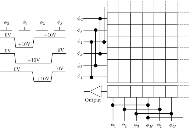
All the gate electrodes in the array are connected by row so that a single contact is made that spans the entire row. The pixels are separated into columns by the introduction of “channel stops”, regions of heavily doped silicon in the regions between pixels in the row. Additionally, each phase of each pixel is linked by phase number in the column direction (in the row direction for the horizontal registers) so that the gates are synchronized. This minimizes the number of voltage clock drivers needed for operation. This is illustrated in figure 1.5 along with a typical voltage clocking cycle. Each row of the image is transferred into the horizontal shift registers one line at a time. Between line shifts, the horizontal registers are completely read out pixel by pixel at the output node.
1.2.1
Charge Generation and Collection
The arrival of photons is proceeded by the generation of charge carriers by the photoelectric effect. The photons may either enter through the polysilicon electrodes (front-side illuminated) or through the bulk silicon (back(front-side illuminated). Front-(front-side illuminated devices have the drawback of losing a portion of the photon flux due to the presence of the front-side circuitry. Backside illuminated devices do not have this issue although they must be backside thinned during manufacture to minimize the distance that photo-generated charge carriers must travel to reach the buried channel (described in [14]). They are also generally more expensive. The benefit of having a backside illuminated device is then its Quantum Efficiency (QE). This is the percentage of incident photons that are detected. QE depends on the reflectivity, device thickness, depletion width, and device resistivity.
Once generated, charge diffuses through the silicon to where it is then collected in the buried channel. The maximum amount of charge that can be held in the buried channel potential well is defined as the Full Well Capacity (FWC). Early CCDs had FWCs of around 6 × 10⁴e− whereas today for the same pixel sizes of 15µm, FWC can be up to 5 ×
Figure 1.5 CCD array clocking operation and electrode wiring.
1.2.2
Charge Transfer
The end of the collection stage is the end of the CCD “exposure”. The readout sequence starts with the transfer of charges to the output electronics. Charge in a given pixel is transferred vertically down the array column into the horizontal shift register and then across to the output node. Each row is transferred simultaneously and each pixel is digitized sequentially. The primary measure of performance in this stage is the Charge Transfer Efficiency (CTE). This parameter is a major subject of this work and factors influencing CTE are discussed in sections 3.1 and 4.1. CTE is defined as the fraction of charge conserved after transfer from one pixel to the next. Therefore, the further a pixel in the array is from the output node, (in terms of number of transfers) the more it will be affected by CTE issues.
Often Charge Transfer Inefficiency (CTI) will be quoted for a CCD instead of CTE and these quantities are related by the relation, CTI = 1 − CTE. Among the several factors
Output
1 0V
0V
+10V +10V
0V
0V 0V
+10V
increasing CTI, the presence of lattice defects is the most challenging as they are both naturally forming during the manufacturing process, and unavoidable under radiation exposure. In this thesis we will explore how much of an issue this is for a new backside illuminated CCD and how to get around it — this is important for radiation-damaged CCDs.
1.2.3
Output Circuit
The final stage is part two of the readout process which involves the charge measurement and digitization. The schematic of a single stage voltage buffer output is shown in figure 1.6. This configuration is termed a source-follower or common-drain amplifier (with the addition of a reset switch). The output node on a CCD is a floating capacitor so that the voltage across this capacitor is defined by the charge that is dumped on its plates (from the last horizontal pixel). The charge on the output or sense node is converted to a voltage at the output. In the CCD used for this work, the output consists of a two stage capacitively coupled source-follower design for low noise performance and high responsivity.
It is at the output where various noise sources are introduced, since up until then there is no uncertainty in the amount of charge contained in a charge packet (aside from Poisson noise in the size of the charge packet, and a very small fraction of charge left behind due to trapping).
Figure 1.6 Standard CCD on-chip output circuit schematic (source-follower).
1.3
Noise Sources
Dark current
As mentioned earlier, the valence-conduction bandgap is comparable to the molecular scale factor for energy, 𝑘𝑇 so that charge carriers can be promoted between bands thermally. This leads to the generation of signal without illumination which is indistinguishable from photo-generated charges. The mean dark current can be measured and subtracted but there is no such remedy for its noise which exhibits Poisson noise. This dark current has various sources within the CCD and has been studied in great detail as it is an inherent feature of the silicon. Primarily, dark current emanates from the channel surface oxide interface (due to the large concentration of trapping states) and the depletion region [19]
It is ultimately roughly an exponential function of temperature so devices are typically cooled to minimize the dark current effects to a manageable level. In addition to cooling, gate electrodes may also be operated in inverted mode. During inversion, minority carriers enter from the channel stop region to the surface, recombining with majority carriers that are thermally generated, leaving only bulk material to contribute to the dark current.
Figure 1.7 Representative CCD output video waveform showing CDS sampling process.
The addition of noise from dark current comes from both the inherently probabilistic nature of the thermal charge generation and also from the Dark Signal Non-Uniformity (DSNU). DSNU refers to the variability of dark signal production rate from pixel to pixel since each pixel will have some structural uniqueness. This also gives rise to pixels producing abnormally high levels of dark current which are termed “hot pixels” – highly undesirable features in a CCD.
Signal noise
The discretization of charge and photons leads to shot noise (first introduced by Walter Shottky in 1918). It is given as 𝜎shot=√𝑆 where 𝑆 is the expected signal level. The SNR
Single pixel cycle Reset pulse
feedthrough
Reset level
Signal level Reference
Signal
V
olta
ge
of a given signal level only accounting for shot noise is thus also √𝑆. For small signals this is a problem and so exposures are lengthened to boost signal, 𝑆 and thus, SNR. Another signal noise source is introduced by the same cause of DSNU which is called Pixel Response Non-Uniformity (PRNU). This is the variability of sensitivity to light from pixel to pixel.
kTC noise
The operation of the reset switch after the measurement of each pixel value leads to a thermally generated noise source otherwise known as Reset noise. The voltage across the output node capacitor relative to the reference level gives the value of the pixel. This reference level, however, is a fluctuating quantity due to thermal activity due to the
channel resistance of the reset transistor. The noise term in units of e- is given as √𝑘𝑇 𝑞⁄
where 𝑞 is the electronic charge (1.6 × 10⁻¹⁹C) and is the output node capacitance.
Reset noise is countered by the application of Correlated Double Sampling (CDS). In this method, two output samples every pixel cycle, one once the output has been reset and one after signal has been dumped onto the node. Individually, each measurement is affected by noise but the difference will not be since the measurements are correlated. This difference takes the variation in reset level out of the equation. In figure 1.7 the samples used from a representative output waveform from a CCD for the CDS operation are shown.
Read noise
medium) and Flicker noise (which has a pink noise PSD, caused by trapping states in the Si-SiO2 interface). The output amplifier is typically Flicker noise limited at low readout
speeds of 100kHz and below, whereas it is Johnson noise limited for higher speeds. Read noise is reduced by frame averaging.
1.4
Photon Transfer Function
The acquisition of the photon transfer function for a CCD camera is one of the most important parts of the characterization process and is discussed at length in [18]. This function describes the relationship between the input (electrons) and output (digital numbers) of the electronic signal chain. From the photon transfer curve (PTC), numerous performance measures may be derived such as read noise, gain constant, FWC, amplifier responsivity and more. Without extolling the merits of the PTC too much, the basics of how to construct one are as follows.
The mean number of electrons registered by the CCD per pixel, 𝑛𝑒 after a given exposure time, can be found from the recorded mean number of DN per pixel, 𝑛𝑠, and is related to
𝑛𝑒 by,
𝑛𝑒 = 𝑔 ⋅ 𝑛𝑠
where 𝑔 represents the gain of the CCD in electrons/ADU. Since 𝑛𝑒 obeys Poisson statistics the noise in the number of arriving photons in a pixel, 𝜎𝑛
𝑒 = √𝑛𝑒. The measured noise,
𝜎𝑛
𝑠 is defined as follows:
𝜎𝑛𝑠
2 = (𝜎 𝑛𝑒⁄ )𝑔
2
+ 𝑟2 = (√𝑛
Here, 𝑟 represents the read noise (and possibly other sources of noise). So 𝜎𝑛2𝑠 ∝ 𝑛𝑠, where the constant of proportionality is 1 𝑔⁄ .
The variance of the number of ADU in a pixel, 𝜎𝑛𝑠
2 is found from a pair of illuminated flat field images. Many pairs of flat field images are used to calculate the value of 𝑔, each pair at a different exposure time (and hence different values of 𝑛𝑠). It is required in each frame to subtract the bias level of the CCD and the dark current accumulated in the same exposure time. This necessitates the acquisition of a ‘dark’ frame (shutter closed) for each pair of flat field images. Each flat field image is then adjusted by subtracting from it, the dark frame image. Then, the variance calculated from the difference of the two images in a pair is equal to 2𝜎𝑛2𝑠. The mean number of counts in each frame in a pair is averaged to give 𝑛𝑠.
1.5
Radiation Damage
(Rutherford scattering) that can cause defect clusters whose size depends on the incident particles’ energy.
It should be noted that the type of damage that this work is concerned with is of the permanent type — transient effects are also possible, such as the creation of ionization tracks, which will affect any number of exposures and then dissipate after some time. Permanent damage can refer primarily to either surface or bulk material damage and figure 1.8 illustrates some of these mechanisms of damage. At the surface, one type of high energy particle damage results in the creation of e-h pairs in the SiO2 as shown in [15]; in this
case, mobile electrons are swept into the buried channel whereas the holes remain in the oxide, generating an electric field which is equivalent to an electrode voltage change. Another type of surface damage results in the increase in the number of band-gap energy states caused by dangling bonds at the Si-SiO2 interface; this leads to an increase in the
amount of dark current produced, although it can be mitigated by inverted mode operation.
atoms and the final situation consists of clusters of Frenkel pairs and vacancy defects that migrate in the lattice to form stable defect configurations with impurity/dopant atoms such as carbon, phosphorus, boron or oxygen. These are the defects that diminish CTE and are (indirectly) the subject of Chapters 3 and 4 of this work, where, a more thorough discussion of lattice defects is presented.
Figure 1.8 Types of radiation damage (adapted from [19]).
2
The WaSP instrument
2.1
Introduction
The Wafer-Scale camera for the Prime focus of the 200-inch Hale telescope (WaSP) was developed to succeed the Large Format Camera (LFC) at the Palomar observatory on Palomar mountain. The instrument’s purposes are
1. To boost the P200 imaging capabilities by providing better QE, noise performance, speed, and image quality, lowering maintenance overhead all with modern components;
2. To overcome limitations and problems that LFC presented such as instrument freezes, image gaps, low speed, outdated software, and low astrometric distortion and;
3. To provide a testbed for the development of detector software and output electronics that will be used for the Zwicky Transient Facility (ZTF) [7].
electronics (mounted directly on the camera) and passed onward through fiber optic cabling from the prime focus to the instrument computer on the telescope dome floor. Figure 2.1 displays the general arrangement of components on the instrument.
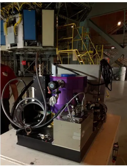
Figure 2.1 WaSP camera dewar with mounted Archon electronics.
2.2
Design
Figure 2.2 (cutaway) Detector housing contents showing main e2v CCD, lateral thermal shielding
and braided thermal cold link.
2.2.1
Mechanical and thermal
Figure 2.3 Detector housing contents showing CCDs,
thermal shield (shown semi-transparent) and fixtures.
CCD controller (mounted to the instrument dewar). In figure 2.1, The top half (purple) in this figure contains the liquid nitrogen tank that provides cooling power to the focal plane located in the bottom portion via a flexible thermal link. This thermal link is pictured in the cutaway of figure 2.2.
Figure 2.4 Cooling cycle showing expected cooling time and temperature
differentials between sensor locations.
Figure 2.5 .(cutaway) Internals of LN2 dewar section showing cold
finger (center) which interfaces with thermal link shown in figure 2.2.
Furthermore, wire thicknesses for temperature sensors and heat resistors were minimized. Wiring, however, presented an optimization problem in that the thinner a wire becomes, the lower the conducted heat transfer – but also the higher the temperature of the wire becomes, resulting in higher a higher radiated power over the length of the wire. Thermal radiation presents the largest source of input thermal power, entering from the dewar window and walls. The design therefore incorporates shielding around the detector assembly as shown in figures 2.2 and 2.5.
An iterative thermal model was constructed, based on the relevant material densities, conductivities, emissivities, heat capacities, and view factors. This allowed the calculation of the detector temperature and its “hold-time” given a full tank of LN2, given an ambient
indeed, the observed hold-time in normal use at the observatory is measured to be 24 hours, on average.
Figure 2.6 Pump-down cycle showing expected time to vacuum (start of cooling).
2.2.2
Signal chain
Figure 2.7 Focal plane layout in the context of the Hale telescope prime focus FOV with CCD
output channels indicated (all dimensions in mm). All CCDs have a common pixel pitch of 15µm.
From figure 2.7 it is shown that the WaSP detectors have a total of 8 outputs which required 2 ADC cards on the Archon controller. Each e2v chip output is a two-stage source follower design (as described in figure 1.6) with a user defined second stage load resistance. The STA chips have a single stage output with a user defined load resistance. Output amplifier responsivities and loads used are given in table 2.1.
Table 2.1 On-chip amplifier responsivity (vendor specification).
The e2v CCD is equipped with replica dummy outputs for each output for common mode rejection (CMR). This is performed by differential pre-amplifiers installed on the vacuum
CCD Responsivity (µV/e-) Load resistance (kΩ)
e2v 7 5
interface board before reaching the Archon controller. The STA chips are not so equipped, so the 4 redundant outputs (due to their frame transfer mode of operation) on their illuminated side were used for CMR. The simplified pre-amp schematic is shown in figure 2.8 with resistance values in table 2.2. The pre-amp gain is then (𝑅1+ 𝑅2+ 𝑅 ) 𝑅⁄ 2, thereby allowing an estimate of the electronic gain of the system; these numbers are given in table 2.2. Note that the gains listed for the on-chip amplifiers are estimates only and have not been measured directly. It is based on the assumption that a single stage source-follower is typically expected to have a gain of approximately 0.8.
Figure 2.8 Simplified VIB differential pre-amp schematic.
Table 2.2 Electronic gain calculation for output electronics for the WaSP CCDs.
e2v STA
On-chip amplifier 0.8 0.8
VIB pre-amplifier (0.15 + 1 + 0.15) 1⁄ = 1.3 (1.5 + 1 + 1.5) 1⁄ = 4
System (expected) 62.5 𝜇𝑉 𝐷𝑁⁄
1.3 ⋅ 0.8 ⋅ 7 𝜇𝑉 𝑒⁄ −= 6 . 9 e
−⁄DN 62.5 𝜇𝑉 𝐷𝑁⁄
4 ⋅ 0.8 ⋅ 7 𝜇𝑉 𝑒⁄ −= 2.2 e −⁄DN
+
–
+
–
𝑅
𝑅2
𝑅 𝑉
2.3
Detector performance
Most characterization for the detectors was performed using the same simple experimental setup consisting of a timing controlled LED in a dark box. Various characteristics of the detector were investigated and some of those results are given here.
2.3.1
Characterization
Photon Transfer
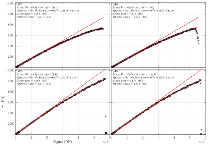
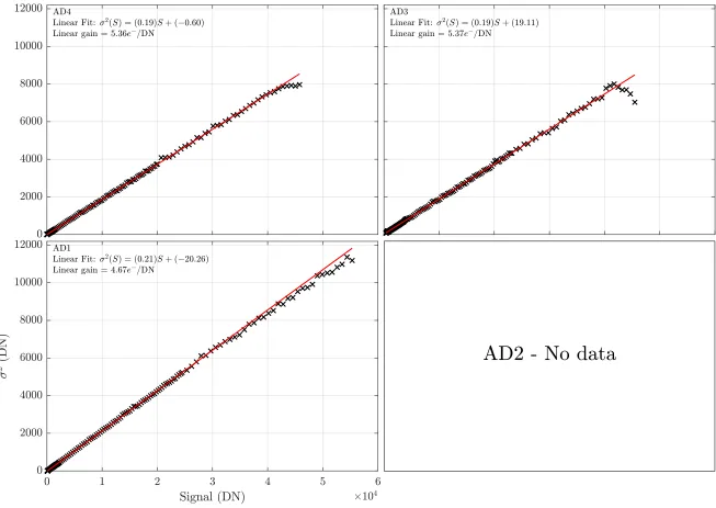
The photon-transfer curves (PTC) for all CCDs were generated using the “shutter-less photon transfer” method described in [19]. In this method a mechanical shutter is not used and the detector is continuously exposed during readout. This produces a ramped illumination profile in the vertical direction in the image due to each row having an exposure time proportional to its distance to the horizontal registers. Each row is then collapsed into a figure of mean signal and variance, thereby giving enough data for a PTC within a single frame. One can also do away with the need for frame differencing since the fixed pattern noise contained in a single row is small. PTCs for the main e2v science and STA guider/focus CCDs are presented in figures 2.15 and 2.16.
modelled by a quadratic function of the form 𝜎2 = 𝛾𝑆 − 𝜈𝑆2, where 𝛾 defines the gain (DN/e-) and 𝜈 is a non-linearity parameter. These fits are included in figure 2.15 along
with the linear fits for comparison, and it is seen that there is a non-trivial difference between the gain estimations from each fit. The STA guide/focus CCDs do not seem to exhibit as much PTC non-linearity despite having a similar dynamic range and identical pixel pitch. Additionally, as noted in [1], whether the device is of the high-𝜌 deep depletion variant has no bearing on the extent of this effect.
Figure 2.9 Charge collection region (simulation) cross-section of CCD from [1]. Black
potential field lines are changed to the red when a 50ke- charge packet is introduced at
the location indicated by the red spot. The right-most pixel then becomes smaller.
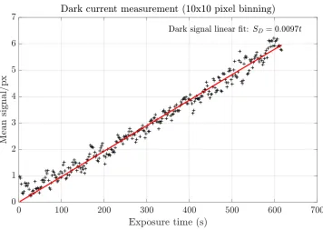
Dark current
“exposure” time. The result is shown in figure 2.17 and the mean dark signal is measured as 9.7 × 10− DN/s for a 10 by 10 px region of the sensor at a temperature of 165K. Converting this to the appropriate units, we have,
(9.7 × 10− DN/s × 5.9 e-/DN)
100 px × 1 hr = 2.1 e
-/px/hr
The quoted dark signal by e2v is 3 e-/px/hr at 173K so this measurement is in line with
expectations.
Linearity
parameters, such as signal sampling window size, also have influence on linearity, and this can be a point of further investigation.
Figure 2.10 Spot grid projected image on the WaSP guider CCD with a substrate bias of 40V.
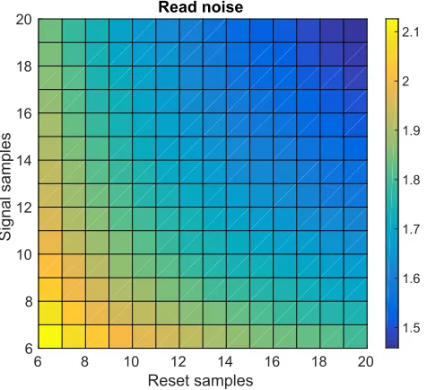
Read noise
it is shown that if the reset or signal sampling window widths need to be traded (keeping the total pixel time constant) it can be done with an insignificant penalty in read noise.
Figure 2.11 Mean PSF FWHM using an isotropic Gaussian fit of all spots in
figure 2.10 plotted as a function of back bias voltage.
Back-bias verification
2.3.2
Challenges
PTC bump
Under certain conditions related to the parallel gate voltages, PTC anomalies are introduced in the form of variance dips. An example of this is shown in figure 2.14. This effect has been noted in at least one other detector characterization campaign [8]. In that study it was noted that the dips appeared when the phase collection voltage was set to a level between 2V and 4V. The dip is seen as a sudden reduction in noise at a particular signal level before resuming the expected linear trend until full well. This indicates the occurrence of charge mixing once a certain signal threshold is reached, which also ceases beyond another threshold, as noted in research presented in [9]. The dip has been observed to occur in a wide range of signals in the range depending on the chosen collection and barrier phase voltage levels.
Malfunctioning STA CCD output
All attempts to read data from AD2 on the STA CCD designated as the focus chip on WaSP proved unsuccessful. This resulted in AD3 being the sole output for this detector thereby limiting the focus chip frame-rate. Inspecting the video signals from all outputs revealed very slow settling times which has so far eluded explanation (figure 2.12). Furthermore, from AD2 it was seen that the signal level was relatively unchanged with respect to the reset level regardless of the level of illumination.
Figure 2.13 Reset feed-through pulse height (DN) as the RG high and low levels are varied. Pulse
height increases until threshold voltage, 𝑉𝑇, but then decreases.
draining the sense node of charge and allowing a measurement of the (no charge) reference level. The sense node will respond to RG voltage changes (the feed-through) so long as the switch is closed.
Figure 2.14 e2v Photon transfer curve exhibiting a noise “dip” at 4.3 × 10⁴e-. The dip
appears at different signal levels depending on the parallel gate voltages used.
Figure 2.13 shows the result of this test. For a given RG-lo value, the reset pulse height increases with RG-hi up to a maximum and then decreases. This maximum occurs consistently at 9V indicating that this is the threshold voltage, 𝑉𝑇 of the reset MOSFET. The behavior that is not expected, however, is the gradual reduction in the RFT pulse height with increasing RG-hi value — it is expected that the RFT remains at a constant height beyond 𝑅𝐺,ℎ𝑖= 𝑉𝑇. This occurs to the point where if 𝑅𝐺,ℎ𝑖 is high enough (with
Figure 2.17 Mean dark counts per second per 10 x 10px region of the CCD.
Figure 2.18 Linearity performance of the e2v sensor for all outputs showing
[image:48.612.138.509.406.657.2]Figure 2.19 e2v CCD read noise (in DN with a conversion gain of 5.8e-/DN) as a
function of number of samples taken in the signal and reset windows of the video waveform.
2.4
Integration at Hale telescope
Figure 2.20 WaSP instrument with peripheral components.
[image:50.612.69.272.47.312.2]Figure 2.21 Hale 200” telescope with primary mirror (bottom) prime focus (top) and equatorial mount (right to left).
Figure 2.22 WaSP being lowered into the prime focus cage.
Figure 2.23 Composite r’,g’,i’ tricolor first-light images taken during camera commissioning.
Im
age c
re
dit:
Ju
stin
Be
lick
[image:50.612.69.274.360.634.2] [image:50.612.350.530.360.704.2]The instrument was intended to allow for auto-guiding and auto-focus using the peripheral STA CCDs. Additionally, capability for sub-array fast readout and dithering modes are also requirements which necessitated careful CCD waveform timing arrangements to facilitate all modes of operation. The Waveform Definition Language [20] was used extensively for this purpose and has enabled several customizable use modes for the camera in conjunction with the included software GUI.
Figure 2.24 Assembled WaSP focal plane pictured with (left to right) the author,
Principle Electronics engineer, R. Smith, and COO Mehcanical engineer, Alex Delacroix.
2.5
Delta-doped CCDs
the WaSP imager. Currently the only other project utilizing delta-doped scientific CCDs is the Faint Intergalactic Redshifted Emission Balloon (FIREBALL-2) mission [12]. This experimental 1m telescope-on-a-balloon contains a fiber-fed UV spectrograph and is the second iteration of an experiment to study the intergalactic and circumgalactic medium emission. A successful flight was conducted in September 2018, although results are yet forthcoming. In the meantime, the science benefits offered by exceptional QE performance from delta-doped CCDs are still to be discovered.
Figure 2.25 Photon absorption depth in Si as a function of wavelength, taken from [19].
2.5.1
Delta-doping principles
The formation of the Si-SiO2 interface in CCDs results in the presence of fixed positive
field-free region (which then diffuse toward the back surface). According to figure 2.25, the absorption depth of UV photons (100 nm < 𝜆 < 300 nm) is between 1 and 10 nm whereas the backside potential well can extend up to 1 µm past the interface. This presents a problem for QE in the UV range since charge is likely to be swept into the backside well and recombine with surface states instead of proceeding further in the silicon to be collected in the signal channel. A significant fraction of charge generated by absorption beyond the backside well is also lost of there is no back-surface processing to negate the charge generated by oxide growth.
Figure 2.26 Pixel slice through the depth of a CCD showing the effect of 𝛿-doping.
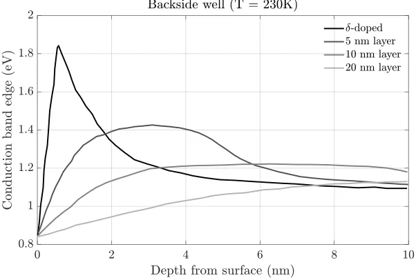
its permanent nature and its effectiveness (down to shorter wavelengths). The principle, in short, is that by the application (via Molecular Beam Epitaxy) of a monatomic layer of boron (resembling a 𝛿-function) on the backside of the CCD (subsequently protected by a 2.5nm layer of Si), the backside potential well thickness can be confined to be less than 1 nm. This is because this implanted boron layer acts as a sheet of negative charge. The effect of different layer thicknesses is illustrated in figure 2.27, taken from [13]. The narrowest monatomic “𝛿-doping” layer yields a backside well thickness of around 0.7nm.
Figure 2.27 Shortening of the backside potential well as the implanted
Boron layer becomes thinner, taken from [13].
2.5.2
Sensitivity measurements on-sky
[image:55.612.236.414.292.365.2]To show that the laboratory demonstration of delta-doped sensors can be reproduced on-sky, a test was conducted to measure the sensitivity boost offered when observing blue objects with the 2k×2k delta-doped CCD, normally used as a guider in WaSP. Four standard star targets were selected (listed in table 2.3) of which three were blue and one red; the red target was chosen as a point of comparison.
Table 2.3 B – V magnitude for standard stars tested (3 blue and 1 red).
Target B – V magnitude
Hz44 – 0.406 Feige92 – 0.308 Hz43 – 0.372 Ross627 0.231
Since the sensors are located differently on the focal plane as depicted in figure 2.7, vignetting and spatial variation of filter leak needed to be taken into account. To this end, each target was imaged at various positions from edge to edge of the focal plane — figures 2.30 and 2.31 show the locations each target was imaged at for both the r’ and u’ filters.
Assuming all vignetting and filter leak effects can be eliminated, we may (roughly) predict the expected sensitivity boost for a standard star in a given filter offered by the delta-doped sensor. This is done by combining the known spectral flux density for each target,
Boost factor = ∫ (𝑓𝑡(𝜈) ⋅ 𝐹𝜈 ⋅ 𝑄𝐸𝑔(𝜈)) 𝑑𝜈 ∞
−∞
∫ (𝑓𝑡(𝜈) ⋅ 𝐹𝜈⋅ 𝑄𝐸𝑚(𝜈))𝑑𝜈 ∞
−∞
⁄ (2.1)
[image:56.612.174.474.359.563.2]Before going on sky, flat field and bias calibration frames were taken, which may also give an indication of the differences in sensitivity between the two sensors. Figure 2.34 depicts a u’ band flat-field signal (for a 60s exposure time to the high lamps in the dome) color map of a portion of the focal plane on a shared color scale. Figure 2.33 shows the same in r’ band (for a 30s exposure time). The sensitivity increase is evident in the u’ flats. Figures 2.32 and 2.35 further show corresponding sample column profiles across both sensors. In r’ band the guider and main chip are matched in QE so the flat field continues the roll-off profile in the guide chip. In u’ band, however, there is a jump in measured signal.
Figure 2.28 Filter transmission (u’ g’ and r’ filters) and QE curves from [17].
increased – this is most likely due to filter leak which is more pronounced closer to the edges of the filter. Filter leak is apparent for both filters used. This data can be used to estimate the filter leak profile as a function of radial distance, since as per figure 2.29 taken from [31] vignetting of the prime focus image does not come into play within the radial distances considered here.
Table 2.4 Expected u’ band sensitivity boost from the delta-doped sensor.
Target Expected
boost
Hz44 1.75 Feige92 1.69 Hz43 1.76 Ross627 1.68
The distinction between fluxes measured on the guider and main chip are indicated in the plots. Aperture photometry was done according to the standard method described in [16] with a generous 15 pixel FWHM central aperture. It was seen that PSFs on the guider chip were generally taller, indicating less charge diffusion than on the main science chip. Frames were not flat-fielded and all pixel values were converted to absolute units of e-.
result. Further investigation is required to determine the actual band-pass of the filters used for observations and whether any other losses are at play.
Figure 2.29 P200 Prime focus FOV vignetting profile (from [31]) with
100% and 75% line markers indicated in both left and right figures.
2.6
Summary
Figure 2.30 Target imaging locations on the focal plane in r’ filter.
[image:60.612.165.451.407.690.2]Figure 2.32 Column slice of r’ band flat across both guider and a portion of the main chip.
[image:61.612.179.434.385.665.2]Figure 2.34 Color map of u’ band flat across both guider and a portion of the main chip.
[image:62.612.130.486.447.690.2]Figure 2.36 Aperture photometry for Feige92.
[image:63.792.65.749.72.520.2]Figure 2.37 Aperture photometry for Hz43.
Figure 2.38 Aperture photometry for Hz44.
[image:63.792.65.379.77.281.2]3
Trap pumping investigation of the E2V CCD231-C6
3.1
Introduction
In this chapter we describe the method and results of a CTE investigation performed using the WaSP camera (which utilizes new un-damaged CCDs). Specifically, the limitation on CTE presented by bulk lattice traps is explored, with detailed general-population characteristics of these traps. Bulk traps are a certain type of trap and traps are one factor among others that affect CTE. The existence of bulk traps, however, is the primary CTI causing effect in modern CCDs.
Figure 3.1 Waveform timing diagram (for a 3-phase device) showing
overlap and slew-rate requirements.
CTE is the measure of a CCD’s efficiency in transporting a charge packet from one pixel to the next ie. the fraction of a charge packet size (number of charge carriers) transferred. The parallel and serial registers are usually made with differently sized phases and are operated separately. Thus, CTE must be measured separately for both. As described in section 1.2.2, charge is transferred across phases by appropriately raising and lowering electrode potentials to storage and barrier states. To ensure good CTE, electrode voltage
Slew rate
slew times must be sufficiently low, otherwise blooming will occur. At the same time, phase overlap must be sufficiently high (higher than the charge diffusion time constant) to ensure decent CTE. This is depicted in figure 3.1.
Figure 3.2 Source of process and design traps. Indicated, is a bump in the potential field
profile caused by a process defect.
Factors that determine CTE are
Fringing field drift: This is the shape of the electric field near the edges of the phases. Fringing fields must be managed properly by defining appropriate clock slew-rates and clock levels.
Self-induced drift: This is the effect of mutual repulsion of charge carriers. This effect is the first to take effect during the charge transfer process.
Thermal diffusion drift: This is thermal scattering of charge. Temperature is the governing parameter of this effect and it is dominant in the absence of the aforementioned two. The effect decreases with decreasing temperature (despite carrier mobility increasing due to settling of the lattice structure).
Once the above effects are managed by tuning the CCD gate voltages, the remaining CTE limiting factor is to do with traps located in the signal channel. Generally, this is the case in modern CCDs, since when using manufacturer recommended gate voltages and timings,
-V +V -V +V
[image:65.612.247.420.167.269.2]CTE is routinely in the range of 0.99999 and 0.999999 (although this figure is dependent on signal level, as will be elaborated on in chapter 4).
3.1.1
Trap formation, locations and effects on data
Traps can be classified into the following four categories:
1. Design traps 2. Process traps 3. Bulk traps 4. Radiation traps
The first two types trap charge by means of an alteration in the electric potential field in the path of charge transfer. This is depicted in figure 3.2. Design traps are those that are caused by improper design features. This most usually occurs in areas of the CCD where electrodes vary in width, causing a constriction in the signal path. With bad specification, this area may result in a potential “bump”: a design trap. Process traps on the other hand are potential “bumps” caused by errors in the manufacturing process. These are errors such as the peeling of the edges of polysilicon gates and dopants being injected in places they should not. Design and process traps are capable of trapping on the order of tens to thousands of electrons. As quite a mature technology, CCDs are nowadays relatively immune to these things.
on the purity of the silicon and – in the case of traps caused by radiation damage – the incident radiation flux density. Since CCDs are normally manufactured using high quality silicon, bulk traps are typically not a concern for ground-based astronomy since CTE is good enough except in very high precision applications. Radiation caused traps on the other hand are almost always a concern. As will be demonstrated, for bulk and radiation traps, trap capture and emission is dependent on pixel clock rate, temperature, charge packet size, and charge packet density.
Even as CCD manufacturing standards rise, so too do their requirements for the purpose of precision astronomical measurements. Lattice traps remain the next challenge to overcome in terms of improving CTE. High-precision radial velocity measurement by ground based instruments is a prime case in point as described in [21]. It was determined that CTI was responsible for shifts in measured radial velocity of several m s-1. The remedy
[image:67.612.251.400.520.620.2]used was to calibrate the effect and correct it during data reduction. A limitation of this approach, however, was that the CTI dependence on signal level was not completely understood and hence not faithfully modelled, causing uncertainty in the correction.
Looking to space applications, CTE is, for example, an unsolved challenge to the Euclid mission (undertaken by ESA) which will be making precise galaxy shape measurements (using the VISible imaging instrument) for weak gravitational lensing studies [32]. According to simulations, for a p-channel CCD, the mission will exceed the shape measurement error budget within four years solely due to diminishing CTE. The situation is much worse for n-channel CCDs which are more susceptible to radiation damage due to the different mechanisms for creating traps for holes and electrons. For the WFIRST coronagraph which is to perform direct imaging of exoplanets, the expected planet signal is at most a few electrons [28]. Extensive work is underway to determine how to retain this signal as it traverses the silicon on the way to the output amplifier. All approaches are being considered to tackle this issue – from hardware modifications (introducing notched signal channels) to optimized clocking, modeling and post facto correction and also simply lengthening exposure times (at the expense of observing cadence).
3.1.2
Types of traps in CCDs and mechanism of CTI
Trapping in CCDs is generally modelled using the Shockley-Read-Hall model for the rate of carrier generation and recombination (also known as trap-assisted generation and recombination) [35]. This process consists of four sub-processes and these are depicted in figure 3.4. According to this model,
𝑈 = 𝑝𝑛 − 𝑛𝑖
2
𝑝 + 𝑛 + 2𝑛𝑖⋅ cosh (𝐸𝑖𝑘𝑇− 𝐸𝑡)
𝑁𝑡𝑣𝑡ℎ𝜎 (3.1)
where 𝑈 is the net rate of generation/recombination (carriers s-1 cm-3), 𝑁
𝑡 is the trap density (cm-3) at energy level 𝐸
cross section (cm2), 𝑣
𝑡ℎ is the thermal velocity (cm s-1), 𝑇 is temperature (K) and 𝑛, 𝑝 are the concentrations of free electrons and holes respectively (cm-3) [19]. A positive 𝑈 indicates
[image:69.612.229.421.197.322.2]a net recombination of electron-hole pairs and a negative 𝑈 indicates a net generation of electron-hole pairs.
Figure 3.4 Recombination and generation processes modelled by equation (3.1).
From this relation, the carrier lifetime can be expressed as,
𝜏𝑐= 1 𝑁𝑡𝑣𝑡ℎ𝜎
(3.2) where 𝜏𝑐 is the capture time constant in an exponential decay process. The emission time constant, 𝜏𝑒 is defined as,
𝜏𝑒 = 1
𝑁𝑐𝑣𝑡ℎ𝜎exp ( 𝐸
𝑘𝑇) (3.3)
where 𝑁𝑐 is the density of conduction band states (cm-3). The thermal velocity 𝑣
𝑡ℎ is given by,
𝑣𝑡ℎ= √3𝑘𝑇 𝑚⁄ 𝑒,𝑐 (3.4)
where 𝑚𝑒,𝑐 is the electron effective mass for conductivity (𝑚𝑒,𝑐= 0.26𝑚0 where 𝑚0 =
9.11 × 10− 1 kg, the rest mass of an electron). The density of conduction band states is given by,
𝑁𝑐= 2 ⋅ (2𝜋 ⋅ 𝑚𝑒,𝑑⋅ 𝑘𝑇
ℎ2) 2⁄
(3.5)
where 𝑚𝑒,𝑑 is the electron effective mass for calculation of density of states (𝑚𝑒,𝑑=
1.08𝑚0).
From the point of view of CCD charge transport, it is the capture and emission time constants that are of critical importance. The probability of capture/emission within the interval [0, 𝑡] of a given trap in a CCD is then,
𝑃𝑐,𝑒= 1 − exp(− 𝑡 𝜏⁄ 𝑐,𝑒) (3.6)
where 𝑡 is the dwell time (s) of the carrier in the vicinity of the trap. These time constants can be measured on a trap by trap basis for a CCD and thus, by then deriving the corresponding energy level of the trap from Eq.(3.3) the trap can then be identified by cross-referencing the literature on known silicon trap characteristics.
Figure 3.5 Silicon lattice point defects. (a) Vacancy, (b) Divacancy, (c) Self-interstitial, (d)
Interstitialcy, (e) Interstitial impurity, (f) Substitutional impurity, (g) Impurity-Vacancy pair, (h)
Impurity-Self-interstitial pair.
In recent work on CCD traps, extrinsic point defects resulting from an un-irradiated CCD have been identified [37]. Based on an assumed cross section 𝜎, two defects purported to match those found in pocket pumping experiments are stated to be the carbon-interstitial-phosphorus-substitution (CiPs) and the boron-interstitial-oxygen-interstitial (BiOi). These
are traps with energy levels closest to those calculated from the trap time constants measured at different temperatures. However, since the number of traps resulting from impurities are so numerous and span a large range of energy levels it becomes difficult to speculate on the identity of any particular trap. Furthermore, identification of such bulk traps has since been limited to very few efforts as most groups have directed their efforts to investigating radiation damage traps which result in intrinsic point defects (vacancies and self-interstitials).
(a) (b)
(c)
(d)
(f) (e)
(g) (h)
3.2
Trap characterization
Traditionally, the technique of Deep Level Transient Spectroscopy (DLTS) is used to characterize charge carrier traps in semiconductors. In this method, a voltage is pulsed across a diode of the semiconductor connected in reverse bias to fill traps in the depletion region. During trap thermal emission, a transient capacitance is induced due to the recovery of the trap charge states. The measurement of this capacitance is repeated for varying voltage pulse frequencies and from this data, a ‘resonance’ frequency can be identified where the measured transient capacitance is maximum. This reveals the energy level of the trap species. A limitation of this method is that all trap species are probed at the same time. However, the Laplace DLTS technique overcomes this by employing Laplace transforms to delineate species by energy level [46]. Nonetheless, DLTS results are only used as a cross-reference here as CCDs are not amenable to this method.
The silicon E and A center defects are variations of the Si self-interstitial defect while the two divacancy defects are the single and double donor configurations of the same defect. One of the defects has yet to be identified. The functions 𝜏 (𝑇 ) that these values of 𝜎 and
𝐸 yield according to Eqs (3.2 – 3.5) are depicted in figure 3.6. It should be noted that p-channel CCDs are susceptible to different species of defects that can be found in [11].
Table 3.1 CCD radiation traps – known energy levels and cross-sections in the literature.
D efect 𝑬𝒕 (eV ) 𝝈 (cm2) Si-E 0.46 5 × 10⁻¹⁵ (V-V)- 0.39 2 × 10⁻¹⁵ Unknown 0.3 – 0.34 5 × 10⁻¹⁶ (V-V)-- 0.21 5 × 10⁻¹⁶ Si-A 0.17 1 × 10⁻¹⁴
Table 3.2 CCD pre-irradiation traps – known energy levels and cross-sections in the literature.
Defect 𝑬𝒕 (eV ) 𝝈 (cm2)
CiPs (III) 0.23 3 × 10⁻¹⁵ BiOi 0.27 5 × 10⁻¹⁶ CiPs (IIB) 0.32 1.5 × 10⁻¹⁴
Pre-irradiation defects have been identified in the references ([37] and [6]) although these defect species attributions are speculative due to the error bounds on the calculated energy levels. Nonetheless, these are tabulated in table 3.2 below. The carbon-phosphorus defect complex has five configurations according to [29] and two of these are suspected to be CTE causing traps. The remaining trap is a combination of interstitial boron and oxygen.
3.2.1
Pocket pumping
from. It is a powerful technique, first used to characterize traps by pixel location and size (number of electrons trapped) [19]. This is accomplished by exposing the CCD to a flat field and then clocking the image forwards and backwards by a certain number of phases/pixels over and over again. During the process, traps are filled when a charge packet surrounds it and emit when the charge packet has left. The packet which the emitted charge joins depends on whichever packet is closest. Thus, if charge is ‘pumped’, it is transferred from a given pixel to either the preceding or subsequent pixel/packet (see figure 3.8). After pocket pumping, one can expect an image such as that in figure 3.7 (left).
Figure 3.6 Radiation traps from table 3.1 – emission time constants as a function of
temperature according to equations (3.2 – 3.5)and trap parameters 𝐸 and 𝜎.
dark pixel with a subsequent bright one. Traps in phase 3 (not pictured) will pump ‘forwards’ producing a dark pixel with a preceding bright one. Traps in phase 2 will not pump. This is because the closest charge packet to any trap in phase 2 is always the originating packet. Traps in phase 2 can be probed by the sub-scheme 2-3-1’-3. Of course, in this scheme, traps in phase 1 are also probed (again) but they can be differentiated from those in phase 2 by the orientation of the dipole. All sub-schemes combined comprise the pumping scheme for the device.
Figure 3.7 Left: Pocket pumped image sample. Right: Column plot (of mean subtracted
signal counts) clearly showing a trap dipole at row 40.
Examples of unconventional pumping schemes to account for such variations can be found in [39] and [6].
Figure 3.8 Sub-scheme (1-2-3-2) for a three phase pumping scheme showing a trap in phase 1 that is pumping. Traps in phase 3 (not shown) will also pump in the same way.
A pocket pumped image from a CCD should in principle have a uniform dipole density across the image because the trap density is also constant. This density, however, will be determined by the flat-field signal level used for pocket pumping. This is because the mean charge packet size defines the volume of silicon probed in each pixel and thereby the probability of a trap encounter. The trap volume density is then 𝑁𝑡∕ (𝑁𝑝⋅ 𝑉𝑐) where 𝑁𝑝 is the number of pixels, 𝑉𝑐 is the charge packet volume, and 𝑁𝑡 is the total number of dipoles (traps) found. The flat-field signal therefore must be set high enough to see a decently representative number of traps. However, if set too high it may take an unreasonable number of pumping cycles to produce measurable dipoles above the shot
Pixel 1
Pixel 2
Pixel 3
– Trap – Charge packet
T
im
e
Interval
noise. Furthermore, if there is significant flat-field variation, there will be a commensurate variation in the density of traps revealed across the device.
3.2.2
Trap parameters
After pocket pumping 𝑁 cycles (typically on the order of thousands), one can expect column profiles such as that in figure 3.7 (right). Each dipole is composed of bright and dark pixels with levels 𝑆1 and 𝑆2 DN, measured relative to the local mean level. The dipole intensity, 𝐼 of a given trap is then 𝐼 = |𝑆1− 𝑆2| 2⁄ ; the amount of signal ‘pumped’ which is a measure of the pumping efficiency. According to figure 3.8, a trap pumps if trapped charge is emitted in the interval, 𝑡𝑝ℎ < 𝑡 < 2𝑡𝑝ℎ. By equation (3.6), the probability of emission in this interval is,
𝑃𝑒(𝑡𝑝ℎ < 𝑡𝑒𝑚𝑖𝑡 < 2𝑡𝑝ℎ) = exp (− 𝑡𝑝ℎ
𝜏𝑒) − exp (− 2𝑡𝑝ℎ
𝜏𝑒 )
Thus assuming that a trap captures 𝐷 electrons in each pump cycle with a probability of capture 𝑃𝑐, the dipole intensity is given by 𝐼 = 𝑁𝑃𝑐𝑃𝑒𝐷. So as a function of the phase time, 𝑡𝑝ℎ,
𝐼(𝑡𝑝ℎ) = 𝑁𝐷𝑃𝑐[exp (−𝑡𝑝ℎ 𝜏𝑒
) − exp (−2𝑡𝑝ℎ 𝜏𝑒
)] (3.7)
By repeating the pocket pumping experiment for varying values of 𝑡𝑝ℎ, the dipole intensity
𝐼 can be measured (example in figure 3.9) and then 𝐼(𝑡𝑝ℎ) fitted by least-squares to determine 𝜏𝑒 (and 𝑃𝑐 and 𝐷) for a given trap. Typically, 𝐷 = 1e-.
the use of equation (3.3) to employ least squares fitting in order to obtain the two parameters, 𝜎 (the capture cross sectional area) and 𝐸 (the trap energy level below the conduction band; 𝐸 = 𝐸𝑐− 𝐸𝑡). Peaks in the histogram of traps in terms of their energies and cross sections should correspond to known trap parameters documented in a reference such as [29]. Once the atomic composition of the trap is known, its behavior under various conditions can be predicted and its formation can even possibly be limited at the manufacturing point of the CCD.
Figure 3.9 Sample dipole intensity curve for a single trap pumped at different frequencies (phase
times, 𝑡𝑝ℎ (𝜇𝑠) ). By fitting equation (3.7) to this, 𝜏𝑒 can be determined.
![Figure 1.8 Types of radiation damage (adapted from [19]).](https://thumb-us.123doks.com/thumbv2/123dok_us/8120850.239350/29.612.170.480.228.430/figure-types-radiation-damage-adapted.webp)
![Figure 2.25 Photon absorption depth in Si as a function of wavelength, taken from [19].](https://thumb-us.123doks.com/thumbv2/123dok_us/8120850.239350/52.612.170.479.283.489/figure-photon-absorption-depth-si-function-wavelength-taken.webp)