COMMISSfON
OF
THE
EUROPEAN
COMMUN-ITIES
Energy
-.
.
A desk calculator controlled measuring system
for the determination of the differential capacitance
of semiconductor-liquid junctions
Blow-up from microfiche original
COMMISSION OF THE EUROPEAN COMMUNITIES
Energy
A desk calculator controlled measuring system
for the determination of the differential capacitance
of semiconductor-liquid junctions
1978
W. Gissler
Joint Research Centre lspra Establishment - Italy
1. Introduction
An important parameter of a semiconductor-electrolyte junction is
its flat band potential Ufb• This is the semiconductor electrode
potential mesured relative to a reference electrode at which the
internal electrical field in the space charge laver disappears and
where correspondingly the energy bands become flat (see e.g. ~1~).
The knowledge of Ufb or of its corresponding semiconductor Fermi
energy level
E~b*)
allows the determination of the energeticposi-tion of the band edges at the interface which is known to be
inde-pendent or only slightly deinde-pendent of the electrode polarization.
Ufb is of great importance because the kinetics of charge transfer
process at semiconductor electrQPes depends essentially on the
re-lative energy position of the redox couple and the band edges.
In semiconductor-liquid junction solar cells Ufb is of particular
importance for efficiency and stability considerations (see e.g. {-2~).
The question of whether or not photoelectrochemical water
decompo-sition is possible depends essentially on how far Ufb is more
nega-tive than the reversible hydrogen electrode potential.
So far only an approximate method for the calculation of Ufb of
me-tal oxide semiconductors in contact with aqueous electrolytes has
been foundL-3~. To obtain reliable values an experimental
determi-nation is indispensable. The most common method is based on the
mea-surement of the differential space charge capacity dC/dU ~4-6~.
Usually dC/dU is measure~ by comparing the space charge capacitance of the semiconductor electrode with a kno\vn capacity in a bridge
cir-cuit. However this is a rath~r time consuming method and allows only
*) The electrochemical potential U is related to the energy E which
is used in semiconductor physics by
U = -e (E + 4.5)
the measurement in steady state conditions. Faster methods based on
. a potential pulse method /.:8
J
and a network analyzer /_-9J
have '"'been'"'c!evelop.ed .recently. In this work a new fast measuring systemis presented which ··±s controlled by a process calculator and which is based on the measurement of the phase·''/ shift ·and' 'amp"ri'tuae·--·()f~-a~~smali .
ac-voltage.
Principles
The determination of the flat band potential Vfb is based on the
Matt-Schottky relation for the space charge capacity C and the electrode
potential U (see e.g. ~10~).
(1)
t and
c
are the dielectric constants of the semiconductor and the0
vacuum respectively. Nd is the donor density and the other constants
have their usual meaning.
Extrapolation of measured values of 1jc2 to zero gives U(l/C2--iio- 0)
=
Ufb• Additionally Nd can be determined from the slope d(ljc2)/dU. Equ. (1) is completely valid only for ideally polarizable electrodes.This condition is for semiconductor electrodes usually satisfied in
the dark and by using indifferent electrolyte solutions under anodic
for n-type and cathodic bias for p-type materials.
The determination of C requires the knowledge of the total equivalent
electrical circuit of the electro-chemical cell which is composed of
the semiconductor electrode, the electrolyte and the counter
elec-trode. It contains capacitors due to the double layers of the
semi-conductor and the counterelectrode, due to surface states and the
space charge layer and it contains resistances due to the bulk
electrolyte and the bulk semiconductor. However this complicated
and often incompletely known circuit can be approximated at
fre-quencies which are large in comparison to reciprocal relaxation
times of surface states
(>
l04s-
1) by the simple circuit consistingonly of the space charge capacity C and one res is tor T in serie
LS
J .
Therefore at frequencies in the order of 104Hz and higher
conventio-nal capacity measurement techniques can be used for the
investiga-tion of the space charge capacity of a semiconductor electrode in an
electrochemical cell.
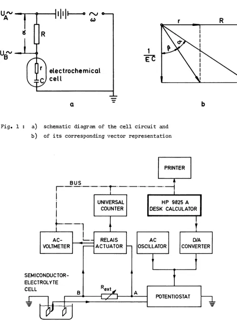
Measurement method
The space charge capacity C is determined by a measurement of the
phase shift~ and the amplitudes UA and UB of an ac-voltage which
is superimposed on a de voltage as shown in fig. la. From the vector
diagram of Fig. lb the following relation can be derived:
1 R coscx
EG =
-s~in_(,..ot_+...,~"'~")---s~i~n-(l2
~
=
arctgL
ctgcx- L/sinoJ1'
=
tan@EG
(2)
(3)
(4)
E is the ac-frequency and L
=
lzcelJ / fZtotf • This ratio is ob-tained from the ratio of the ac amplitudes UB and UA.In fig. 2 the measurement system is shown which includes as central
part the desk calculator (HP 9825 A) by which most of the peripheral
instruments are controlled, the calculation of the data is performed
and tables and plots by the printer (HP 9871) are generated. The
ac-and de- voltages are applied through the external inputs of the
po-tentiostat (PAR 373). The de-voltage is obtained from a digital to
analog converting power supply (HP 59303 A). The ac-amplitudes UA
and UB are measured at the points A and B respectively in the
ac-vol-tage mode of the digital multimeter (HP 3455 A) and the phase shift
is measured by a universal counter (HP 5328). To trigger the counter
for start and stop the zero passage of the sine waves at A and B
respectively are monitored. In order to avoid reading errors also
mea-sured by the multimeter in the R-mode and the universal counter
re-spectively. For a rapid connection of the measurement instruments to
their respective circuits a relay actuator (HP 59306.A) also is used.
A schematic diagram of the relay actuator and the instruments which
are switched by it is shown in fig. 3 which contains also a table of
the relay state during the specific instrument operations. The
sym-bol A stands for a connection of the terminal C with A whereas B is
used for the opposite state. The step numbers correspond to the order
in which they are programmed to be passed.
Step 1 and 2 are only once passed whereas steps 3 to 5 are repeated
for each electrode potential setting.
Program description
The calculator program which controls the measurement sequence,
pro-~eeds the data and generates tables and plots, is written in the
HPL-language. The address codes and the meaning of the used program code
sets are listed in Table 1. The program itself is listed in annex 1;
it consists essentially of 5 parts:
1) line 0 to 42:- This part serves for the input of data and its
ta-bulation by the printer. The input data
"date", "electrode", electrolyte", and "remarks" are optional and
are to characterize the electrode under measurement
dielectric constant, xL-6~, and electrode surface, Swill be
used for the calculation of the space charge capacity per unit
surface area and of the charge carrier density according to (1)
initial and final potential V ~2~ and V ~3~ define the
boun-daries of the electrode potential range, whereas N is the number
of intervals in which this range is subdivided and measurements
are performed. V ~1~ is the electrode potential which is
app-lied after the measurement sequence has been performed. X ~1~
the ac·-frequency, E, and the external resistance, R, are
mea-sured by program control
K ~6~ is a control parameter; if the value 2 is entered, the measurement sequence which starts from the initial potential
v
;_·-2
.J
to the final potential V /_-3J
is complemented by a se-cond serie from V /_-3J
to V["'2J.
At V j_'-3J
only one measure-ment will be performed.2) line 43 to 62: By this part the particular operations for the
program code setting, potential setting, measuring of phase shift
and amplitude are controlled.
3) line 63 to 107: The measuring data determined in_part 2) are
pro-cessed according to the relations (2), (3) and (4) in order to
ob-tain the capacitance and resistance values. Finally a last square
fit is performed to obtain the values for the flat band potential
and the charge carrier density. It is supposed that the l/C2
-u
dependence is linear. The program part 2) to 3) can be repeatedup to 5 times according as x/_-2_7 is set equal to 1 or not. The
generation of a table is optional and is controlled by the
para-meter
x['"4J
("1" for the affirmative case).4) line 107 to 166: This part controls the generation of the
Matt-Schottky plot. A normalization of the l/C2-scale is performed
such that the maximum l/C2-value is printed at least at 50% of
the length of the y-axis. Also the potential scale is normalized;
the boundaries are given by the integer values of the initial and
final potential. If more than one measuring series have been
per-formed the plot symbols are different for each serie.
r:)
) I line 167 to 246: Here the subroutines are stored, which are stan-dard subroutines for the plotting program with the exception of
Results
The described system was tested by measurements on CdS and Fe 2
o
3 semiconductor electrodes. Table 2 shows the results as obtained witha single crystalline CdS/lm Na
2
so
4 electrode in the tabulated form as generated by the calculator. Fig. 4 is the correspondingMatt-Schottky plot as generated by the calculator. As time period x L-1~
of two consecutive measuring points 1 s has been chosen. The
mini-mum time is determined essentially by the ac-voltage measurement and
is about 0.2 s. The obtained 1jc2 versus U plot is linear in the
vol-tage range -0.5<. U
<
0.2. By the least square fit method a flat band potential Ufb=
-0.76V(SCE) and a charge carrier density of N0
=
2.4 • 1016 cm-3 is obtained. Both values are in good agreement withear-lier measurement ~12~ and with the specifications of the crystal
respectively.
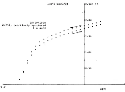
The measurements on Fe
2
o
3 have been performed in the measuring mode corresponding to a I~6~ value setting of 2 which effects amea-surement sequence from the initial to the final and back to the
ini-tial potenini-tial. The electrode has been prepared by reactive
sputte--2
ring of Fe
2
o
3 powder in ano
2 atmosphere of 10 Torr on an iron substrate. The electrolyte was an aqueous solution 1 m NaOH Fig. 5shows the calculator generated Mott-Schottky plot. It is interesting
to note the small difference between the measuring points obtained
du-ring the anodic and cathodic "sweep". These differences are probably
caused by small changes of the surface composition causing slight
changes also of capacity values. These differences are themore
pro-nounced the faster the sweep rate is analogously to vol tametric
mea-surements. For potential values
u<-
0.5 V (SCE) Fe3
o
4 is known to be the stable ph~se ~11~. The deviation from the linearity arelarge for U
>-
0.5 V (SCE); however, from the measured values in the lower electrode potential part a linear extrapolation is possible bywhich for the flat band potential a value of Ufb =-0.82 V (SCE) is obtained in comparison to - 0.73 V (SCE) for sintered polycristalline
Conclusions
A new system for capac~ty measurements which is controlled by a
pro
-cess calculator has been assembled. The system allows a rapid
genera-tion of a Mott-Schottky plot. It can be used in an analogous mode as
in voltametry measurements to monitor changes of the surface state
Table
1
Instrument
Address
program
code
operation
multimeter
R2F4AOHOM3T3
resistance
meas.
722
HP
3455A
R3F2AOHOM3T3
fast
ac-voltage
m.
universal
counter
PF4G6T
frequency
meas.
725
HP
5328
A
PF
:
G4R
phase
shift
me
as.
relay
actuator
59303
A
716
"Aa"
or
"Ba"(
a=relay
N)
relay
state
digital
analog
719
"EO"
range
setting
converter
HP
59303
A
718
v
(v
=
potential)
potential
setting
Printer
HP
9871
701
-Table II
S_t).'\CE CdARG~ CAPACirY' t:IIALUAr!Ut~ r'PJM Hi? 9325 C(U'fRvLLP.D P•ii\.St: SHIF'f ME~SURt:r.JEN'fS
measurement :~o 1
Ux(\1) delay(ns] delay(degrJ Vv(V) llx(V)
0.100 2212.378 ' 38.890 0.150 0. 07.) 0.075 2222.331 39.065 0.153 0.071
o. 050 2234.649 3 9. 232 0.156 0.071 0.025 2239.401 39.365 0.158 0.071
O. J:>a 2243.393 39.435 0.161 0.071 -o.a25 2251.174 39.572 0.163 J. a72 -a. 05u 2255.571 39.649 0.165 0.072 -0.075 2256.945 39.674 0.168 0.072 -0.100 2260.264 39.732 0.171 0.072 -0.125 2262.140 3!}. 765 0.173 0.072 -0.150 2265.132 39.817 0.176 0.073
-o .175 2263.038 39.781 0.179 o.a73 -0.200 2263.137 39.732 0.182 0.073
-0.225 2261.099 39.747 0.185 0.074 -0.250 2265.68~ 39.827 0.183 a.a74 -1).275 2261.253 39.749 0.193 0.074 -0.300 2255.926 39.656 0.195 0.074 -0.325 2243.641 39.528 0.201 o. 075
-u. 35\l 2242.433 39.418 0.205 0.075 -11.375 2234.724 39.2-33 o. 211 0.075 -0.400 2224.765 H.l03 0.215 0.076 -0.425 220L 553 39.823 0.222 0. 076
-a. 450 2194.143 39.570 0.227 0.077 -:).475 2169.866 39.143 o. 236 0.071 -0.5JO 2150.153 37.796 0.242 0.077 -0.525 2113.77() 37.157 0.253 0.078 -0.551) 2081.592 36.591 o. 261 0.078 -J.575 2024.786 35.593 0.274 0. 0 79 -J.600 1978.769 34. 784 o. 2a4 0.078
25/09/1973 Cd3, sinqle crvstal •. 5 fll l'la2SJ4
electrode surface (cm2) S dielectric constant X[6)
freauency (kHz) 8 =
external resistance [Ohm) R
initial potential (V) Vf2) final pctential (V) V(3) = st?ndby octential (V) 11(1) =
number of intervals ~
time between two measurinq ocints (s), X(1)
test 1. 50 10.00 48.83 82.10 0.10 -0.60 -0.50 28.00 1. 00
Vx/VO r (Ohm) C (F /c.n2) l/c2[ cm4/F2)
0.469 24.312 4. 417E-08
o. 462 24.044 4.508E-08
o. 456 23.716 4.608E-08 a. 450 23.562 4. 695E-08
o. 4 4-1 B. 4J3 4. 799E-08 0.439 23.181 4. 8 82E-O<l 0.435 23.030 4. 958E-08 0.428 22.906 5.071E-03 0.425 22.775 5.141E-08
o. 418 22.607 5.277E-08 0.413 22.457 5.366E-08 0.408 2 2. 3 92 5. 465E-08 0.403 22.258 5. 583E-08 0.397 22.154 5. 705E-08 1).392 21.94 7 5. 8078-08 0.3s:J5 21.827 5.9698-08 a.3cl0 21.749 6.105E-08
o. 371 21.58 5 6.325E-08 0.366 21.472 6. 486E-Oc3 0.357 21.248 6. 743E-08 0.353 21.248 6. 859E-08 0.343 21.048 7.18 5E-08 o. 337 20. 961 7. 404£-08
o. 327 20. 794 7. 782E-08 0.319 20. 672 8.075E-08 0.308 20.451 8.609£-08 0.300 20.376 3.994E-08 o. 287 211.120 9. 769E-OB 0.276 19.858 1.046E-07
charge carrier density {cm-3) flat band potential Ufb (V) •
5.126E 14 4.920E 14 4. 710E 14 4. 537E 14 4.342E 14 4.196E 14 4.0S9E 14 3.388E 14 3.784E 14 3.592E 14 3. 473E 14 3.348E 14 3.209E 14 3. 072E 14 2.9668 14 2.807E 14 2.683E 14 2.50\lE 14 2. 371E 14 2.199E 14 2.12 5E 14 1.937E 14
1. 824E 14 L651E 14 1.534E 14 1. 349E 14 1. 236E 14 1. 048E 14 9.148E 13
References
£"1J H. Gerischer, in "Physical Chemistry'', Vol. LXA,
H.
Eyring, D. Henderson, andw.
Jost, Editors, AcademicPress, New York (1970)
~2J H. Gerischer, J. electroanalyt. Chem. 82, 133 (1977).
~3J M.A. Butler, and D.S. Geriley, J. Electrochem. Soc., ~·
228 (1978)
~4J M. Ho£mann-Perez, and H. Gerischer,
z.
Elektrochem.,Ber. Bunsenges. physik. Chern. 65, 771 (1961).
~5J
R.
Hemming, Philips Res. Repts 19, 323 (1964).C6J
M.J. Madou, F. Cardon a. W.P. Gomes, J. Electrochem. Soc.ill·
1623 (1977).£7J
J.H. Iennedy, and Iarlw.
Frese, Jr., J. Electrochem.Soc. 125, 723 (1978).
L8J
M. Brzostowska, M. Milkowska, A. Ialeirowski, ands.
Mine,J.
Electroanal. Chem. ~' 389 (1978).["9
J
M. Tomkiewicz, in "Semiconductor Liquid-Junction Solar Cells, Proceedings o£ a Conference on the Electrochemistry and Physics o£ Semiconductor-Liquid Interfaces under Illu-mination, Airlie, Va., ed A. Heller, Electrochem. Soc., Princeton, N.J. (1977).L-lOJ
R. Memming, Proc. International meeting on Topics in Sur-face Chem. (IBM), (1977), in press.~llJ J. Schets, J. Van Muylder, and M. Pourbaix in "Atlos o£ Electrochemical Equilibria in Aqueous Solutions M. Pourbaix ed., (1966).
~12~
H. Minoura, M. Tsuiki, and T. Oki, Ber. Bunzenges.Fig. 1
Fig. 2
s
E
c
R
electrochemical cell
a
1
EC
a) schematic diagram of the cell circuit and
b) of its corresponding vector representation
I
PRI:TER IBUS .
r·-·-·-·-·-·r-·-·-·-·-·-·----1
1 I
i
I
i
UNIVERSAL COUNTER
HP 9825 A
DESK CALCULATOR
.__·-·-·,
i
.
I
!
'
ib
AC-VOLTMETER
'---·- RELAIS
r--- ACTUATOR
-AC OSCILLATOR
0/A
CONVERTER
EM! CONDUCTOR- • LECTROLYTE
ELL
8 Rext~ A
~
I1-'
1 I /I
OJ
~.
POTENTIOSTAT
~
[image:14.598.51.518.132.766.2] [image:14.598.92.477.403.764.2]potentiostat
universal
counter
Cell
E
frequency
R
external
resistance
0.phase
shift
®
UA
ac-voltcige
at
A
Ue
ac-voltage
at
B
©
instrument
StepN
me
as.
relay
state
®
univ.
counter
1
E
A
multi
meter
2
R
A
univ.
counter
3
Ol
A
multi
meter
4
UA
B
multi
meter
multi
meter
5
Us
A
Fig. 3 : schematic diagram of the relay actuator and its peri-pheral instruments. The inserted table gives the relay state corresponding to the operation which is performed during the different steps.A
A
A
A
B
8
A
A
A
B
A
A
B
A
A
CdS,
-1.0
single crystal .5 m Na2S04
/ / / ,It ,-* /
•*
•*
l/C*C[cm2/F2].•*
It ·It It It * I t
•*
It It It
* *
•*
l.OOE 15
8.00 6.00 * It * It 4.00 2.00 U[V]
Fig. 4 Matt-Schottky plot o£ a CdS/lm Na
2
so
4 electrode as printedaccording to the program
25/09/1978
~e2~3, reactively sputtered 1 m NaOH
* -1.0 * It * * * It It It It
*
l/C*2[cm2/F2]
It
~
It * * * *
It * ·~
* * * It * * *
2.50E 12
2.00
*
It * * *
*
* *
1.
so
1. 00
o.sa
U[V)
[image:16.598.87.520.65.385.2] [image:16.598.84.510.482.797.2]ANNEX: Progam List
J : J i lll X [ 1 0
J ,
V ( 1 0 ] , i< ( 1 0 J1 : r err: 7 1 S 2 : w r t 716 , ·• A 111
, .. A 2 •• , .. A 3 .. I •• A 4 " , " A 5 ·•
3: fmt 3/,2Sx,"SPACE CclARGB CA~AC£TY 8VAL0ATIO~ ",z:wrt 701
4: fmt dFRJ~ clP 9d25 C0~~HOLLED @tiAS~ SHl~£ M8A3UR8MB~~S11
:wrt
701
5: fmt 25x1Sl"=",2/:wrt 701
6: dim A$[12] 1d$[120] ,C$[120] 10$[120]
7: ent "date (12) 11 ,A$
d: ent "electrode? [120]",B$
9: ent "electrolyte ?"1C$
lJ: ent .. remarks ., [120) ..
,u$
11: frnt cl2U,/1cl20,/,cl20,/1cl20
ll: wrt 7011A$,B$ 1:$1D$
13: ent "dielectric constant ?11
1X[6]
14: ent "electrode surface [c~2] 11
1S
15: ent "initial potential [V] 11
1V[2]
16: ent "final potential (~] 11
1 V(3]
17: ent 11Standoy potential [V] 11
1 ~[1]
lJ: ent "numoer of intervals"1N
19 : e n t •• if 1 oop r e q u • en t K [ 6 ] + 2 " , K [ 6 )
20: if K[6]#2:l+K{6)
21: dim 3[21~+1] ,Q[S,2 .. ~+1] ,A[5,2A.~+1] ,3[5,2lJ+l] ,H[5,2N+l] ,R[512t~+l]
22: dim G [5,2i.~+1]
23: ent ••time betw. 2 meas. points [s]•',X[l]
.24: wrt 72S,"PF4G6i"
25: fmt e12.1
2~: red 725,1!:
27: wrt 716,"Al'',"A2","B3","B4","A5"
28: wrt 722,"R2F4A0rl0rt3T3":trg 722:fmt :wait lOJ
29: red 722 ,R
30: fmt cll2,f8.2
31: wr t 701, "electrode sur face [ cm2]
s
= "
,s
Jl: wrt 7011 .. dielectric constant X[6]
=
",X[6)33: wrt 7ill, .. freguency [kHz] 8 = ",E
34: wrt 7ill,"external resistance [Ohm] R
=
",R35: wrt 70l,"initial potential (V] ~(2] = 11
,V[2)
36: wrt 70l,"final potential [v] V[3] = "IV[3]
37: wrt 701,"standby potential [V] V[lJ = 11 ,V[l]
Jo: wrt 701, "number of intervals N = 11
,J
39: wrt 70l,"time between two measuring points [s], X(l]
=
",X[l]4u: X(l]*lO+X[l]
41: fmt 3,5/
42: wrt 701.3
·13: (\/[3]-\/[2))/J.~+D
44: wrt 719,''EO'' 45: wr t 7 22 1
11
R3F 2AO.d0i\1]'f 3"
45: wrt 725,"P?:G5R11
4 7 : f m t 1 , f 5 • 2.
48: wrt 718.l,v[2];wait luuO
49: l+Z
50: fm t
51: for J=l to K[6]*~+1
52: if J>~:jmp 2
53: V[2]+(J-l)*u+cl[J);jmp 2
55: wrt 718.l,S[J];cll -,time'(J{[l]) 56: wrt 715,"Al",11A2","A3","A4", 11A5u
57: wrt 72s,"~r .. ;fmt fll.3;red 725,1l[Z,J.]
5 d : w r t 716 , "ill .. , " d 2 j• , ., A 3 " , " A 4 •• , " .t3 5 "
.59: trg 722;fmt ;red 722,A[Z,J]
6 0: w r t 71
o, ..
A1" , "B 2" , "A3", "A4 11, "BS"
61: trg 722;fmt ;red 722,u[Z,J]
o2: next J
GJ: for J=l to K[6]*~+1
64: H[~,J]*1e-9*E*le3*360+G[Z,J]
65: d[Z,J]IA[l,J]+L
6 6 : at n (
11
tan ( G [ Z , J ] ) . -LIs in ( G [z,
J J ) ) +w
· 6 7: H* cosO'n
I
(sin (W+G [z,
J1 )
IL-s in (vJ) )
+ .26 8 : i? ·k tan (
v-n
+ H [ ~ ,J1
0 9 :
s ,..
2 ( J:> * 2TT * E * 1 0 0 0 ) A 2 +Q [z ,
J ] • 70: next J71: wrt 718.1,V(l]
7 2 : f m t 2
I ,
1 0 x , .. measurement t'iJ o" , 2 x , z ; w r t 7 0 1 73: fmt f1.0,z;wrt 7lll,Z74: ent "if print required, ent 1" ,X[4]
75: if X[4]#1;jmp 12
76: fmt 2/,10x,"Ux[V]",6x,"de1ay[ns]11,4x,"delay(degr] 11
,5x,"VO.[v.]11,Z;wrt 701
1 7 : £ m t 5 x , "
v
x [ V ] " , 5 x , " VxI
V 0" , 4 x , " r [ 0 h m] " , 7 x , " C [ fI
em 2 ] " , z ; w r t 7 0 17 8: f m t 3x, .. 1/c 2 [em
41
i', 2] ",21;
wr t 70179: for J=1 to K[6]*~+1
80: fmt 2,3f15.3,z 81: fmt 3,4f10.3,z
82: fmt 4,2e15.3
8 3 : w r t 701. 2 ,
s [
J ] , d [z
,J] , G [z,
J1
d 4: w r t 7
u
1. 3, A [z
,J1
,d [z,
J.1 ,
a [ z,
J J1
A [z,
J] , R [ l , J. Jd 5: w r t 7
u
1 • 4 ,11
~ Q [ ~, J J , Q ( ~, J]86: next J
87: fmt
3l;wit
701dd: O+H
89: O•·.r
90: O+ll
91: O+W
92: u+"i/
93: for J=1 to ~+1
94: H+S[Jj*S[J]+H
95: T+3[Jj*Q[Z,J]+£
· 96: U+.::)[J]+LJ 9 7 :
v
+J [z ,
J ] + "9a: next
J-. 93: (.d*V-.C*U) /( (~~+!) *d-U*U) +Q
100: ( 'i'-J* t.J) /d+C
101: 2l(l.602e-19*8.8542e-14*X[6]*C)+w
102: -Q/C+V[4]
103: fmt c10J ,e15. 3
104: wr t 7u1, 11
Charge carrier density [c:n-JJ =" ,vl
105: fmt c100,fl5.2
1
u o :
w r t 7 J 1 , •• f 1 at band pot en t i a 1 U f b [ V ]=
11, V [ 4 ]
107: fmt 4l~wrt 701 lOS: if L.=5; jmp 3
110: if X[2]=l;Z+l+Z;qto 50
111: ent "if plot required, ent l",X[5]
112: if X[5]#1;gto 166
113: max(Q(*] )+r1
114 :
i n t (1
og ( r1 ) )
+1
+ r2
115: ltn"'r2+r3
11
u :
i f r
3I
r 1 < = 2 ; r
3+ r
4 ;1 + r
5 ; jrnp
4117: if r3lrl<=4;r312+r4;2+r5;jmp
3118: if
r3lrl<=8;r314•r4;4+r5;jm~ 2119: r318+r4;8+r5
120: 7Jl•r0
121: ell .,form'(l3.2,10,10)
122: ell 'psiz'(5,10,5,2)
123: v[21•K(1J
124: \/(3j+L<[2]
125: int(min(S(*]))+r6
126: -int(-max(S[*]))+r7
127: ell 'se1'(r6,r7,0,r4)
128: ell 'xaxis'(O,.S,r6,r7)
12 9 :c 11
'yax
is ' (
0 ,r
4I
1 0 , 0 ,r
4 )13
J : e11 ·'move ' (
r 6, 0)131: ell 'skip'(i)
132: ell
·'spaee'(-2)133: fmt f4.l;wrt 70l,r6
134: ell 'move'(r7,0)
135: ell 'skip'(l)
13ci: ell 'space'(-2)
137: frnt f4.l;wrt 70l,r7
138: 2+I;fmt f4.2
139: ell 'move'(O,I*r4ll0)
140: ell 'space'(!)
141: wrt 70l,IIr5;1+2+I;if I<B.S;gto -2
142: ell 'move'(O,lO*r4ll0)
143: ell ·'space' (
1)144: fmt e8.2
145: wrt.70l,r3lr5
146: ell 'move'(r614-.2,10*r4ll0)
147: wrt 701,"1IC*C(crn2IF2J"
14S: ell 'rnove'(r7*314,1.5)
149: ell 'skip'(3)
150: ell 'space'(-3)
151: wrt 7Jl,"U[V]"
152: for I=l to
z
153: if 1=1; 42+C
15 4 :if I=
2 ; 4 3+C
1 55 : if I=
3 ;111 +C
156: if
1=4;120+C
157: if 1=5; 46+C
158: for J=l
to K(6]*~+115
9 :e 11 '
p1
t ' (S [
J ] , Q (I ,
J ) ,C. )
160: next
J161: ell 'move'(-1,0)
162: ell 'skip'(i+3)
163: fmt z;wtb 70l,C;fmt f4.0,z;wrt 70l,I;fmt
164:
ell 'move'(O,O)
16 5:
next
.I166:
end
*9d79
..
167: "time":for M=1 to p1 168: wait 100
169: next M
170: ret 171: .. move" :
172: wtb r0,27 ,65,.int( (pl-X) Ul64.) ,.int( {p1-X)U.) ,int( (p2-Y)V/64), int( (p2-Y)V)
173: ret ·
174: 11
imove":
1 7 5 : w tb r 0 , 2 7 , 8 2 ,. in t ( p 1 U
I
6 4) , in t ( p 1 U ) ,i P. t ( p 2VI
6 4 ) , i n t ( p 2 V) 176: ret17 7: II p1 t t1:
178: wtb r0,27 ,65, int ( {p1-X) Ul64) ,.int( (p1-X)U), int ( (p2-Y.)V/64) ,jr.t ( (p2-Y.)V.) 179: if p3=0;46+p3
180: if p3=46;wtb r0,27,82,0,0,0,6 181: wtb rO,p3;wtb r0,8
182: if p3=46;wtb r0,27,82,0,0,63,-6 183: ret
18 4 : II f p 1 t 11· !
18 5 : w tb r 0 , 2 7 , 9 7 , in t ( ( p1-X) U
I
6 4 ) , i n t { ( p 1- X) lJ ) ,. in t ( ( p 2- Y )VI
6 4 ) , in t ( ( p 2-Y.) V ) 186: if p3=0;46+p3187:
if
p3=46;wtb r0,27,82,0,0,0,6 188: wtb rO,p3;wtb r0,8189: if p3=46;wtb r0,27,82,0,0,63,-6 190: ret
191: 11
ip1t11 :
19 2 : w tb r 0 , 2 7 , 8 2 ,. in t ( p 1
u
I
6 4 ) , in t { p 1 U ) , i n t ( p 2VI
6 4 ) ,.i n t ( p 2 V) 193: if p3=0;46+p3194: if p3=46;wtb r0,27,82,0,0,0,6 195: wtb rO,p3;wtb r0,8
196: if p3=46;wtb r0,27,82,0,0,63,-6 197: ret
198: 11fiplt":
199: wtb r0,27,114,int(p1UI64.) ,int(p1U.) ,int(p2VI64) ,int(p2V) 200: if p3=0;46+p3
201: if p3=46;wtb r0,27,82,0,0,0,6 202: wtb rO,p3;wtb r0,8
203: if p3=46;wtb r0,27,82,0,0,63,-6 204: ret
205: "char":
206: if p2=0; 5+p2; O+p3
207: wtb r0,27,46,p1,int(p2l64),p2,p3 208: ret
209: 11
psiz": 210: p1 +H; p2+vJ
211: wtb r0,27,79,int(p4*120I64.) ,p4*120,int(p3*96l64) ,p3*96 212: ret
213 : II S C 1 11
• :
214: 120WI(p2-p1)+U 215: 96rll(p4-p3)+V 216: p1+X;p3+Y 217: ret
218: .,xaxis":
219: wtb r0,27,46,95,0,5,9
220: if p3=0 and p4=0;X+p3;X+120WIU+p4 221: if p2=0;p4-p3+p2
224: wtb r0,27,114,int(p2U/64.) ,int(p2U) ,0,01wtb r0,43,8;jmp .. (p5+p2•P5)>=p4
225: ret
2 2 6 :
11 y a xis
11 :227: wtb r0,27,46,124,0,3,0
228: if p3=0
and
p4=0;Y+p3;Y+96H/V+p4
229: if p2=0;p4-p3+p2
230: wtb r0,27 ,65, int ( (pl-X)
U/64.),.int( (p1-X)U.) ,.int ( (p3-Y.)V/64.) ,.int ( (p3-Y.)V)
231: p3+p5;wtb r0,43;wtb r0,8
232: wtb r0,27,114,0,0,int(p2V/64.),.int(p2V);wtb r0,43,8;jmp (p5+r2•p5)>=p4
233: ret
2 3 4 : 11
space " :
235: if p1<01gto +2
236: wtb i0,32;jmp 2((p1-l•pl)=Q)
237: wtb
r0,8;j~p(p1+1•p1)=0
238: ret
239: "skip
11 :240: if p1<0;gto +2
241: wtb iO,lO;jmp 2((pl-1•p1)=0)
242: wtb r0,27,10;jmp .(p1+l•p1)=0
243: ret
244: "cspc
11 :245: if p2=0;6+p2
246: wtb r0,27,86,int(96/p2/64),96/p2
247: if p1<0;wtb r0,27,80;ret
.
248: wtb i0,27,72,int(120/p1/64),120/p1
249: ret
250: ''form
11 · :251: wtb r0,27,77
252: wtb r0,27,84
253: if p1=0;13.2•pl;11•p2+p3
254: wtb r0,27,87,int(120*pl/64),120*p1
255: wtb r0,27,76,int(96*p2/64),96*p2
256: wtb r0,27,70,int(96*p3/64),96*p3
257: ret
2 5 tl : II P t YP II :